

SGS Thomson Microelectronics PSD813F1, PSD813F1V Datasheet
Flash In-System Programmable (ISP) Peripherals
FEATURES SUMMARY
■ Single Supply Voltage:
– 5 V±10% for PSD813F1-A
– 3.3 V±10% for PSD813F1-AV
■ Up to 1Mbit of Primary Flash Memory (8 uniform
sectors)
■ 256Kbit Secondary EEPROM (4 uniform
sectors)
■ Up to 16Kbit SRAM
■ Over 3,000 Gates of PLD: DPLD and CPLD
■ 27 Reconfigurable I/O ports
■ Enhanced JTAG Serial Port
■ Programmable power management
■ High Endurance:
– 100,000 Erase/Write Cycles of Flash Memory
– 10,000 Erase/Write Cycles of EEPROM
– 1,000 Erase/Write Cycles of PLD
PSD813F1-A
For 8-bi t MCUs
PRELIMINARY DATA
Figure 1. Packages
PQFP52 (T)
PLCC52 (K)
January 2002
This is preliminary information on a new product now in development or undergoing evaluation. Details are subject to change without notice.
1/3

i
Revision A Flash PSD
PSD813F1-A
Flash In-System-Programmable Microcontroller Peripherals
Table of Contents
1.0 Introduction...........................................................................................................................................................1
2.0 Key Features ........................................................................................................................................................2
PSD813F1 Block Diagram .............................................................................................................................4
3.0 General Information..............................................................................................................................................5
4.0 PSD813F1 Family.................................................................................................................................................5
5.0 PSD813F1 Architectural Overview .......................................................................................................................6
5.1 Memory...................................................................................................................................................6
5.2 Page Register.........................................................................................................................................6
5.3 PLDs.......................................................................................................................................................6
5.4 I/O Ports..................................................................................................................................................7
5.5 Microcontroller Bus Interface..................................................................................................................7
5.6 JTAG Port...............................................................................................................................................7
5.7 In-System Programming.........................................................................................................................8
5.8 Power Management................................................................................................................................8
6.0 Development System............................................................................................................................................9
7.0 PSD813F1 Pin Descriptions ...............................................................................................................................10
8.0 PSD813F1 Register Description and Address Offset.........................................................................................14
9.0 PSD813F1 Functional Blocks.............................................................................................................................15
9.1 Memory Blocks.....................................................................................................................................15
9.1.1 Main Flash and Secondary EEPROM........................................................................................15
9.1.2 SRAM.........................................................................................................................................29
9.1.3 Memory Select Signals...............................................................................................................29
9.1.4 Page Register.............................................................................................................................32
9.2 PLDs.....................................................................................................................................................33
9.2.1 Decode PLD (DPLD)..................................................................................................................35
9.2.2 Complex PLD (CPLD)................................................................................................................35
9.3 Microcontroller Bus Interface................................................................................................................44
9.3.1 PSD813F Interface to a Multiplexed 8-bit Bus ...........................................................................44
9.3.2 PSD813F Interface to a Non-Multiplexed 8-bit Bus....................................................................44
9.3.3 Data Byte Enable Reference......................................................................................................47
9.3.4 Microcontroller Interface Examples............................................................................................47
9.4 I/O Ports................................................................................................................................................52
9.4.1 General Port Architecture...........................................................................................................52
9.4.2 Port Operating Modes................................................................................................................54
9.4.3 Port Configuration Registers (PCRs) .........................................................................................57
9.4.4 Port Data Registers....................................................................................................................60
9.4.5 Ports A and B – Functionality and Structure ............................................................................61
9.4.6 Port C – Functionality and Structure ........................................................................................63
9.4.7 Port D – Functionality and Structure ........................................................................................63
9.5 Power Management..............................................................................................................................67
9.5.1 Automatic Power Down (APD) Unit and Power Down Mode .....................................................67
9.5.2 Other Power Saving Options......................................................................................................71
9.5.3 Reset and Power On Requirement ............................................................................................72

ii
For additional information,
Call 800-832-6974
Fax: 510-657-8495
Web Site: http://www.psdst.com
E-mail: ask.psd@st.com
Revision A Flash PSD
PSD813F1-A
Flash In-System-Programmable Microcontroller Peripherals
Table of Contents
(cont.)
9.6 Programming In-Circuit Using the JTAG Interface ...............................................................................73
9.6.1 Standard JTAG Signals..............................................................................................................74
9.6.2 JTAG Extensions........................................................................................................................75
9.6.3 Security and Flash Memories and EEPROM Protection............................................................75
Absolute Maximum Ratings.........................................................................................................................................76
AD/DC Parameters......................................................................................................................................................77
Example of PSD813F Typical Power Calculation at VCC= 5.0 V.......................................................................78
PSD813F1 DC Characteristics (5 V ± 10% Versions)........................................................................................80
PSD813F1 AD/DC Parameters – CPLD Timing Parameters (5 V ± 10% versions).........................................81
PSD813F1V DC Characteristics (3 V Versions).................................................................................................91
PSD813F1V AC/DC Parameters – CPLD Timing Parameters (3 V versions).................................................92
Timing Diagrams .......................................................................................................................................................100
Programming.............................................................................................................................................................107
PSD813F1 Pin Assignments.....................................................................................................................................108
PSD813F1 Package Information...............................................................................................................................110
Selector Guide...........................................................................................................................................................113
Part Number Construction.........................................................................................................................................114
Ordering Information..................................................................................................................................................114
Product Revisions......................................................................................................................................................115

iii
PSD813F1-A Family Preliminary
For additional information,
Call 800-832-6974
Fax: 510-657-8495
Web Site: http://www.psdst.com
E-mail: ask.psd@st.com
1
1.0
Introduction
Preliminary
Programmable Peripheral
Revision A Flash PSD
PSD813F1-A
Flash In-System-Programmable
Microcontroller Peripherals
The PSD813F1 family of Programmable Microcontroller (MCU) Peripherals brings
In-System-Programmability (ISP) to Flash memory and programmable logic. The result is a
simple and flexible solution for embedded designs. PSD813F1 devices combine many of
the peripheral functions found in MCU based applications:
• 1 Mbit of Flash memory
• A second EEPROM memory
• Over 3,000 gates of Flash programmable logic
• SRAM
• Reconfigurable I/O ports
• Programmable power management.
PSD813F1 devices integrate an optimized “microcontroller macrocell” logic architecture
called the Micro⇔CellTM. The Micro⇔Cell was created to address the unique requirements
of embedded system designs. It allows direct connection between the system address/data
bus and the internal PSD registers to simplify communication between the MCU and other
supporting devices.

PSD813F1-A Preliminary
2
1.0
Introduction
(Cont.)
The PSD813F1 family offers two methods to program PSD Flash memory while the PSD is
soldered to a circuit board.
❏ In-System Programming (ISP) JTAG
An IEEE 1149.1 compliant JTAG interface is included on the PSD enabling the entire
device (Flash memory, EEPROM, the PLD, and all configuration) to be rapidly
programmed while soldered to the circuit board. This requires no MCU participation,
which means the PSD can be programmed anytime, even while completely blank.
The innovative JTAG interface to flash memories is an industry first, solving key
problems faced by designers and manufacturing houses, such as:
• First time programming – How do I get firmware into the flash the very first time?
JTAG is the answer, program the PSD while blank with no MCU involvement.
• Inventory build-up of pre-programmed devices – How do I maintain an accurate
count of pre-programmed flash memory and PLD devices based on customer
demand? How many and what version? JTAG is the answer, build your hardware
with blank PSDs soldered directly to the board and then custom program just before
they are shipped to customer. No more labels on chips and no more wasted
inventory.
• Expensive sockets – How do I eliminate the need for expensive and unreliable
sockets? JTAG is the answer. Solder the PSD directly to the circuit board. Program
first time and subsequent times with JTAG. No need to handle devices and bend the
fragile leads.
❏ In-Application Programming (IAP)
Two independent memory arrays (Flash and EEPROM) are included so the MCU can
execute code from one memory while erasing and programming the other. Robust
product firmware updates in the field are possible over any communication channel
(CAN, Ethernet, UART, J1850, etc) using this unique architecture. Designers are
relieved of these problems:
• Simultaneous read and write to flash memory – How can the MCU program the
same memory from which it is executing code? It cannot. The PSD allows the MCU
to operate the two memories concurrently, reading code from one while erasing and
programming the other during IAP.
• Complex memory mapping – I have only a 64K-byte address space to start with.
How can I map these two memories efficiently? A Programmable Decode PLD is the
answer. The concurrent PSD memories can be mapped anywhere in MCU address
space, segment by segment with extremely high address resolution. As an option,
the secondary flash memory can be swapped out of the system memory map when
IAP is complete. A built-in page register breaks the 64K-byte address limit.
• Separate program and data space – How can I write to flash or EEPROM memory
while it resides in “program” space during field firmware updates, my MCU won’t
allow it! The flash PSD provides means to “reclassify” flash or EEPROM memory as
“data” space during IAP, then back to “program” space when complete.
PSDsoft —ST’s software development tool—now has the ability to generate
ANSI-C compliant code for use with your target MCU. The code generated allows you to
manipulate the non-volatile memory (NVM) within the PSD. Code examples are also
provided for:
• Flash ISP via the UART of the host MCU
• Memory paging to execute code across several PSD memory pages
• Loading, reading, and manipulation of PSD Micro⇔Cells by the MCU
The PSD813F1 is available in a 52-pin PLCC package and a 64-pin plastic Thin Quad
Flatpack (TQFP) package.

Preliminary PSD813F1-A
3
❏ A simple interface to 8-bit microcontrollers that use either multiplexed or
non-multiplexed busses. The bus interface logic uses the control signals generated by
the microcontroller automatically when the address is decoded and a read or write is
performed. A partial list of the MCU families supported include:
• Intel 8031, 80196, 80186, 80C251, and 80386EX
• Motorola 68HC11, 68HC16, 68HC12, and 683XX
• Philips 8031 and 8051XA
• Zilog Z80 and Z8
❏ Internal 1 Mbit Flash memory. This is the main Flash memory. It is divided into eight
equal-sized blocks that can be accessed with user-specified addresses.
❏ Internal secondary 256 Kbit EEPROM memory. It is divided into four equal-sized blocks
that can be accessed with user-specified addresses. This secondary memory brings
the ability to execute code and update the main Flash concurrently.
❏ 16 Kbit scratchpad SRAM. The SRAM’s contents can be protected from a power failure
by connecting an external battery.
❏ Optional 64 byte One Time Programmable (OTP) memory that can be used for product
configuration and calibration.
❏ CPLD with 16 Output Micro⇔Cells (OMCs) and 24 Input Micro⇔Cells (IMCs). The
CPLD may be used to efficiently implement a variety of logic functions for internal
and external control. Examples include state machines, loadable shift registers, and
loadable counters.
❏ Decode PLD (DPLD) that decodes address for selection of internal memory blocks.
The DPLD can also be used to generate external chip selects.
❏ 27 individually configurable I/O port pins that can be used for the following functions:
• MCU I/Os
• PLD I/Os
• Latched MCU address output
• Special function I/Os.
• 16 of the I/O ports may be configured as open-drain outputs.
❏ Standby current as low as 50 µA for 5 V devices, 25 µA for 3 V devices.
❏ Built-in JTAG compliant serial port allows full-chip In-System Programmability (ISP).
With it, you can program a blank device or reprogram a device in the factory or the field.
❏ Internal page register that can be used to expand the microcontroller address space by
a factor of 256.
❏ Internal programmable Power Management Unit (PMU) that supports a low power mode
called Power Down Mode. The PMU can automatically detect a lack of microcontroller
activity and put the PSD813F1 into Power Down Mode.
❏ Erase/Write cycles:
• Flash memory – 100,000 minimum
• EEPROM – 10,000 minimum
• PLD – 1,000 minimum
• Data Retention: 15 year minimum at 90 degrees Celsius (for Main Flash, Boot, PLD
and Configuration bits).
2.0
Key Features
PSD813F1-A Preliminary
4
PROG.
MCU BUS
INTRF.
ADIO
PORT
CNTL0,
CNTL1,
CNTL2
AD0 – AD15
CLKIN
CLKIN
CLKIN
PLD
INPUT
BUS
PROG.
PORT
PORT
A
PROG.
PORT
PORT
B
POWER
MANGMT
UNIT
1 MBIT MAIN FLASH
MEMORY
8 SECTORS
VSTDBY
PA0 – PA7
PB0 – PB7
PROG.
PORT
PORT
C
PROG.
PORT
PORT
D
PC0 – PC7
PD0 – PD2
ADDRESS/DATA/CONTROL BUS
PORT A ,B & C
3 EXT CS TO PORT D
24 INPUT MICRO⇔CELLS
PORT A ,B & C
73
73
256 KBIT SECONDARY
MEMORY (BOOT OR DATA)
4 SECTORS
EEPROM – F1
16 KBIT BATTERY
BACKUP SRAM
RUNTIME CONTROL
AND I/O REGISTERS
SRAM SELECT
PERIP I/O MODE SELECTS
MICRO⇔CELL FEEDBACK OR PORT INPUT
CSIOP
FLASH ISP CPLD
(CPLD)
16 OUTPUT MICRO⇔CELLS
FLASH DECODE
PLD
(
DPLD
)
PLD, CONFIGURATION
& FLASH MEMORY
LOADER
JTAG
SERIAL
CHANNEL
(
PC2
)
PAGE
REGISTER
EMBEDDED
ALGORITHM
SECTOR
SELECTS
SECTOR
SELECTS
GLOBAL
CONFIG. &
SECURITY
Figure 1. PSD813F1 Block Diagram
Preliminary PSD813F1-A
5
3.0
General
Information
The PSD813F1 series architecture allows In-System Programming of all Memory, PLD
Logic and Device Configuration. The embedded Input and Output Micro⇔Cells enable
efficient implementation of user defined logic functions that require both software and
hardware interaction. The devices eliminate the need for discrete ‘glue’ logic, and allow the
development of entire systems using only a few highly integrated devices.
4.0
PSD813F1
Family
All PSD813F1 devices provide these features: 1 Mbit main Flash Memory, JTAG port,
CPLD, DPLD, power management, and 27 I/O pins. The PSD813F1 also adds 64 bytes of
OTP memory for any use (product serial number, calibration constants, etc.). Once written,
the OTP memory can never be altered.
The following table summarizes the PSD813F1:
Part # Flash Additional
No. of Serial ISP Main Memory Memory for
PSD813F1 I/O Micro⇔Cells JTAG/ISC Kbit Boot and/or Data SRAM Turbo Supply
Family Device Pins Input/Output Port (8 Sectors) (4 Sectors) Kbit Mode Voltage
PSD813F1 PSD813F1 27 24/16 Yes 1024 256 Kbit EEPROM 16 Yes 5V
PSD813F1V PSD813F1V 27 24/16 Yes 1024 256 Kbit EEPROM 16 Yes 3V
Table 1. PSD813F1 Product Matrix

PSD813F1-A Preliminary
6
PSD813F1 devices contain several major functional blocks. Figure 1 on page 3 shows the
architecture of the PSD813F1 device. The functions of each block are described briefly in
the following sections. Many of the blocks perform multiple functions and are user configurable.
5.1 Memory
The PSD813F1 contains the following memories:
• A 1 Mbit Flash
• A secondary 256 Kbit EEPROM memory
• A 16 Kbit SRAM.
Each of the memories is briefly discussed in the following paragraphs. A more detailed
discussion can be found in section 9.
The 1 Mbit Flash is the main memory of the PSD813F1. It is divided into eight equally-sized
sectors that are individually selectable.
The 256 Kbit EEPROM or Flash is divided into four equally-sized sectors. Each sector is
individually selectable.
The 16 Kbit SRAM is intended for use as a scratchpad memory or as an extension to the
microcontroller SRAM. If an external battery is connected to the PSD813F1’s Vstby pin,
data will be retained in the event of a power failure.
Each block of memory can be located in a different address space as defined by the user.
The access times for all memory types includes the address latching and DPLD decoding
time.
5.2 Page Register
The eight-bit Page Register expands the address range of the microcontroller by up to
256 times.The paged address can be used as part of the address space to access external
memory and peripherals or internal memory and I/O. The Page Register can also be used
to change the address mapping of blocks of Flash memory into different memory spaces for
in-circuit reprogramming.
5.3 PLDs
The device contains two PLD blocks, each optimized for a different function, as shown in
Table 2. The functional partitioning of the PLDs reduces power consumption, optimizes
cost/performance, and eases design entry.
The Decode PLD (DPLD) is used to decode addresses and generate chip selects for the
PSD813F1 internal memory and registers. The CPLD can implement user-defined logic
functions. The DPLD has combinatorial outputs. The CPLD has 16 Output Micro⇔Cells
and 3 combinatorial outputs. The PSD813F1 also has 24 Input Micro⇔Cells that can be
configured as inputs to the PLDs. The PLDs receive their inputs from the PLD Input Bus
and are differentiated by their output destinations, number of Product Terms, and
Micro⇔Cells.
The PLDs consume minimal power by using Zero-Power design techniques. The speed
and power consumption of the PLD is controlled by the Turbo Bit (ZPSD only) in the
PMMR0 register and other bits in the PMMR2 registers. These registers are set by the
microcontroller at runtime. There is a slight penalty to PLD propagation time when invoking
the ZPSD features.
5.0
PSD813F1
Architectural
Overview
Name Abbreviation Inputs Outputs Product Terms
Decode PLD DPLD 73 17 42
Complex PLD CPLD 73 19 140
Table 2. PLD I/O Table
Preliminary PSD813F1-A
7
PSD813F1
Architectural
Overview
(cont.)
5.4 I/O Ports
The PSD813F1 has 27 I/O pins divided among four ports (Port A, B, C, and D). Each
I/O pin can be individually configured for different functions. Ports A, B, C and D can be
configured as standard MCU I/O ports, PLD I/O, or latched address outputs for
microcontrollers using multiplexed address/data busses.
The JTAG pins can be enabled on Port C for In-System Programming (ISP).
Ports A and B can also be configured as a data port for a non-multiplexed bus or
multiplexed Address/Data buses for certain types of 16-bit microcontrollers.
5.5 Microcontroller Bus Interface
The PSD813F1 easily interfaces with most 8-bit microcontrollers that have either
multiplexed or non-multiplexed address/data busses. The device is configured to respond to
the microcontroller’s control signals, which are also used as inputs to the PLDs. Where
there is a requirement to use a 16-bit data bus to interface to a 16-bit microcontroller, two
PSDs must be used. Section 9.3.5 contains microcontroller interface examples.
5.6 JTAG Port
In-System Programming can be performed through the JTAG pins on Port C. This serial
interface allows complete programming of the entire PSD813F1 device. A blank device can
be completely programmed. The JTAG signals (TMS, TCK, TSTAT, TERR, TDI, TDO) can
be multiplexed with other functions on Port C. Table 3 indicates the JTAG signals pin
assignments.
Port C Pins JTAG Signal
PC0 TMS
PC1 TCK
PC3 TSTAT
PC4 TERR
PC5 TDI
PC6 TDO
Table 3. JTAG Signals on Port C
PSD813F1-A Preliminary
8
5.7 In-System Programming
Using the JTAG signals on Port C, the entire PSD813F1 device can be programmed or
erased without the use of the microcontroller. The main Flash memory can also be
programmed in-system by the microcontroller executing the programming algorithms out
of the EEPROM or SRAM. The EEPROM can be programmed the same way by executing
out of the main Flash memory. The PLD logic or other PSD813F1 configuration can be
programmed through the JTAG port or a device programmer. Table 4 indicates which
programming methods can program different functional blocks of the PSD813F1.
PSD813F1
Architectural
Overview
(cont.)
JTAG Device In-System Parallel
Functional Block Programming Programmer Programming
Main Flash memory Yes Yes Yes
EEPROM memory Yes Yes Yes
PLD Array (DPLD and CPLD) Yes Yes No
PSD Configuration Yes Yes No
Optional OTP Row No Yes Yes
Table 4. Methods of Programming Different Functional Blocks of the PSD813F1
5.8 Power Management Unit
The Power Management Unit (PMU) in the PSD813F1 gives the user control of the
power consumption on selected functional blocks based on system requirements. The PMU
includes an Automatic Power Down unit (APD) that will turn off device functions due to
microcontroller inactivity. The APD unit has a Power Down Mode that helps reduce power
consumption.
The PSD813F1 also has some bits that are configured at run-time by the MCU to reduce
power consumption of the CPLD. The turbo bit in the PMMR0 register can be turned off and
the CPLD will latch its outputs and go to sleep until the next transition on its inputs.
Additionally, bits in the PMMR2 register can be set by the MCU to block signals from
entering the CPLD to reduce power consumption. See section 9.5.
Preliminary PSD813F1-A
9
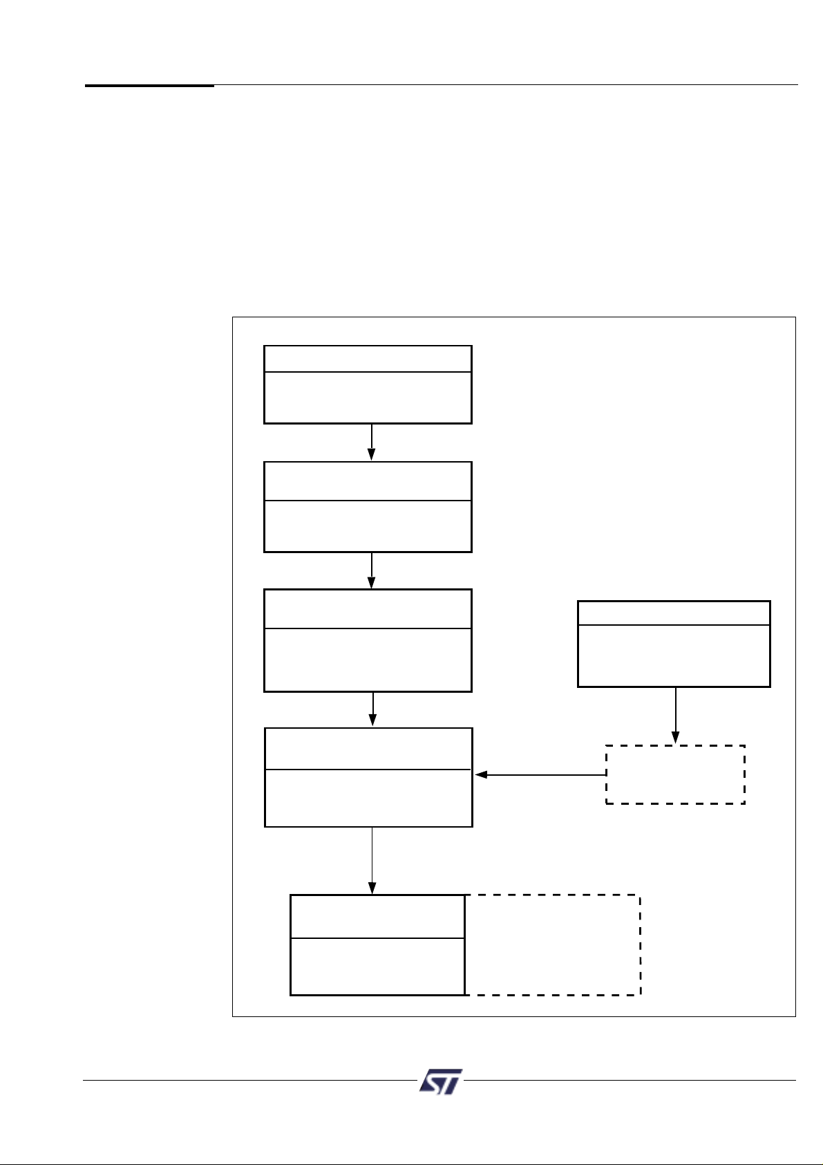
6.0
Development
System
Define General Purpose
Logic in CPLD
Merge MCU Firmware
with PSD Configuration
ST
PSD Programmer
*.OBJ FILE
Point and click definition of
combinatorial and registered logic
in CPLD. Access to HDL is
available if needed.
Define PSD Pin and
Node functions
Point and click definition of
PSD pin functions, internal nodes,
and MCU system memory map.
Choose MCU and PSD
Automatically Configures MCU
bus interface and other PSD
attributes.
PSDPro or
FlashLink (JTAG)
A composite object file is created
containing MCU firmware and
PSD configuration.
C Code Generation
Generate C Code
Specific to PSD
Functions
User's choice of
Microcontroller
Compiler/Linker
*.OBJ file
available
for 3rd party
programmers
(Conventional or JTAG-ISP)
MCU Firmware
Hex or S-Record
format
Figure 2. PSDsoft Development Tool
The PSD813F1 is supported by PSDsoft a Windows-based (95, 98, NT) software
development tool. A PSD design is quickly and easily produced in a point and click
environment. The designer does not need to enter Hardware Definition Language (HDL)
equations (unless desired) to define PSD pin functions and memory map information. The
general design flow is shown in Figure 2 below. PSDsoft is available from our web site
(www.st.com/psm) or other distribution channels.
PSDsoft directly supports two low cost device programmers from ST, PSDpro
and FlashLINK (JTAG). Both of these programmers may be purchased through your local
rep/distributor, or directly from our web site using a credit card. The PSD813F1 is also
supported by third party device programmers, see web site for current list.
PSD813F1-A Preliminary
10
The following table describes the pin names and pin functions of the PSD813F1. Pins that
have multiple names and/or functions are defined using PSD Configuration.
7.0
Table 5.
PSD813F1
Pin
Descriptions
Pin Name Pin* Type Description
ADIO0-7 30-37 I/O This is the lower Address/Data port. Connect your MCU
address or address/data bus according to the following rules:
1. If your MCU has a multiplexed address/data bus where
the data is multiplexed with the lower address bits,
connect AD[0:7] to this port.
2. If your MCU does not have a multiplexed address/data
bus, or you are using an 80C251 in page mode, connect
A[0:7] to this port.
3. If you are using an 80C51XA in burst mode, connect
A4/D0 through A11/D7 to this port.
ALE or AS latches the address. The PSD drives data out only
if the read signal is active and one of the PSD functional
blocks was selected. The addresses on this port are passed
to the PLDs.
ADIO8-15 39-46 I/O This is the upper Address/Data port. Connect your MCU
address or address/data bus according to the following rules:
1. If your MCU has a multiplexed address/data bus where
the data is multiplexed with the lower address bits,
connect A[8:15] to this port.
2. If your MCU does not have a multiplexed address/data
bus, connect A[8:15] to this port.
3. If you are using an 80C251 in page mode, connect
AD[8:15] to this port.
4. If you are using an 80C51XA in burst mode, connect
A12/D8 through A19/D15 to this port.
ALE or AS latches the address. The PSD drives data out only
if the read signal is active and one of the PSD functional
blocks was selected. The addresses on this port are passed
to the PLDs.
CNTL0 47 I The following control signals can be connected to this port,
based on your MCU:
1. WR — active-low write input.
2. R_W — active-high read/active low write input.
This port is connected to the PLDs. Therefore, these signals
can be used in decode and other logic equations.
CNTL1 50 I The following control signals can be connected to this port,
based on your MCU:
1. RD — active-low read input.
2. E — E clock input.
3. DS — active-low data strobe input.
4. PSEN — connect PSEN to this port when it is being used
as an active-low read signal. For example, when the
80C251 outputs more than 16 address bits, PSEN is
actually the read signal.
This port is connected to the PLDs. Therefore, these
signals can be used in decode and other logic equations.
Preliminary PSD813F1-A
11
Pin Name Pin* Type Description
CNTL2 49 I This port can be used to input the PSEN (Program Select
Enable) signal from any MCU that uses this signal for code
exclusively. If your MCU does not output a Program Select
Enable signal, this port can be used as a generic input. This
port is connected to the PLDs.
Reset 48 I Active low reset input. Resets I/O Ports, PLD Micro⇔Cells
and some of the configuration registers. Must be active at
power up.
PA0 29 I/O These pins make up Port A. These port pins are configurable
PA1 28
and can have the following functions:
PA2 27
1. MCU I/O — write to or read from a standard output or
PA3 25
input port.
PA4 24
2. CPLD Micro⇔Cell (McellAB0-7) outputs.
PA5 23
3. Inputs to the PLDs.
PA6 22
4. Latched address outputs (see Table 6).
PA7 21
5. Address inputs. For example, PA0-3 could be used for
A[0:3] when using an 80C51XA in burst mode.
6. As the data bus inputs D[0:7] for non-multiplexed
address/data bus MCUs.
7. D0/A16-D3/A19 in M37702M2 mode.
8. Peripheral I/O mode.
Note: PA0-3 can only output CMOS signals with an option
for high slew rate. However, PA4-7 can be configured as
CMOS or Open Drain Outputs.
PB0 7 I/O These pins make up Port B. These port pins are configurable
PB1
6 and can have the following functions:
PB2
5 1. MCU I/O — write to or read from a standard output or
PB3
4 input port.
PB4
3 2. CPLD Micro⇔Cell (McellAB0-7 or McellBC0-7) outputs.
PB5
2 3. Inputs to the PLDs.
PB6
52 4. Latched address outputs (see Table 6).
PB7
51 Note: PB0-3 can only output CMOS signals with an option
for high slew rate. However, PB4-7 can be configured as
CMOS or Open Drain Outputs.
PC0 20 I/O PC0 pin of Port C. This port pin can be configured to have
the following functions:
1. MCU I/O — write to or read from a standard output or
input port.
2. CPLD Micro⇔Cell (McellBC0) output.
3. Input to the PLDs.
4. TMS Input** for the JTAG Interface.
This pin can be configured as a CMOS or Open Drain output.
PC1 19 I/O PC1 pin of Port C. This port pin can be configured to have
the following functions:
1. MCU I/O — write to or read from a standard output or
input port.
2. CPLD Micro⇔Cell (McellBC1) output.
3. Input to the PLDs.
4. TCK Input** for the JTAG Interface.
This pin can be configured as a CMOS or Open Drain output.
Table 5.
PSD813F1
Pin
Descriptions
(cont.)
PSD813F1-A Preliminary
12
Table 5.
PSD813F1
Pin
Descriptions
(cont.)
Pin Name Pin* Type Description
PC2 18 I/O PC2 pin of Port C. This port pin can be configured to have
the following functions:
1. MCU I/O — write to or read from a standard output or
input port.
2. CPLD Micro⇔Cell (McellBC2) output.
3. Input to the PLDs.
4. Vstby — SRAM standby voltage input for SRAM battery
backup.
This pin can be configured as a CMOS or Open Drain output.
PC3 17 I/O PC3 pin of Port C. This port pin can be configured to have
the following functions:
1. MCU I/O — write to or read from a standard output or
input port.
2. CPLD Micro⇔Cell (McellBC3) output.
3. Input to the PLDs.
4. TSTAT output** for the JTAG interface.
5. Rdy/Bsy output for in-system parallel programming.
This pin can be configured as a CMOS or Open Drain output.
PC4 14 I/O PC4 pin of Port C. This port pin can be configured to have
the following functions:
1. MCU I/O — write to or read from a standard output or
input port.
2. CPLD Micro⇔Cell (McellBC4) output.
3. Input to the PLDs.
4. TERR output** for the JTAG interface.
5. Vbaton — battery backup indicator output. Goes high
when power is being drawn from an external battery.
This pin can be configured as a CMOS or Open Drain output.
PC5 13 I/O PC5 pin of Port C. This port pin can be configured to have
the following functions:
1. MCU I/O — write to or read from a standard output or
input port.
2. CPLD Micro⇔Cell (McellBC5) output.
3. Input to the PLDs.
4. TDI input** for the JTAG interface.
This pin can be configured as a CMOS or Open Drain output.
PC6 12 I/O PC6 pin of Port C. This port pin can be configured to have
the following functions:
1. MCU I/O — write to or read from a standard output or
input port.
2. CPLD Micro⇔Cell (McellBC6) output.
3. Input to the PLDs.
4. TDO output** for the JTAG interface.
This pin can be configured as a CMOS or Open Drain output.
Preliminary PSD813F1-A
13
Table 5.
PSD813F1
Pin
Descriptions
(cont.)
Pin Name Pin* Type Description
PC7 11 I/O PC7 pin of Port C. This port pin can be configured to have
the following functions:
1. MCU I/O — write to or read from a standard output or
input port.
2. CPLD Micro⇔Cell (McellBC7) output.
3. Input to the PLDs.
4. DBE — active-low Data Byte Enable input from 68HC912
type MCUs.
This pin can be configured as a CMOS or Open Drain output.
PD0 10 I/O PD0 pin of Port D. This port pin can be configured to have
the following functions:
1. ALE/AS input latches address output from the MCU.
2. MCU I/O — write or read from a standard output or input
port.
3. Input to the PLDs.
4. CPLD output (external chip select).
PD1 9 I/O PD1 pin of Port D. This port pin can be configured to have
the following functions:
1. MCU I/O — write to or read from a standard output or
input port.
2. Input to the PLDs.
3. CPLD output (external chip select).
4. CLKIN — clock input to the CPLD Micro⇔Cells, the
automatic power-down unit’s power-down counter, and
the CPLD AND array.
PD2 8 I/O PD2 pin of Port D. This port pin can be configured to have
the following functions:
1. MCU I/O — write to or read from a standard output or
input port.
2. Input to the PLDs.
3. CPLD output (external chip select).
4. CSI — chip select input. When low, the MCU can access
the PSD memory and I/O. When high, the PSD memory
blocks are disabled to conserve power.
V
CC
15, 38 Power pins
GND 1,16,26 Ground pins
Port A Port B
Microcontroller Port A (3:0) Port A (7:4) Port B (3:0) Port B (7:4)
8051XA (8-bit) N/A Address [7:4] Address [11:8] N/A
80C251 (page mode) N/A N/A Address [11:8] Address [15:12]
All other 8-bit
multiplexed
Address [3:0] Address [7:4] Address [3:0] Address [7:4]
8-bit non-multiplexed
bus
N/A N/A Address [3:0] Address [7:4]
Table 6. I/O Port Latched Address Output Assignments*
N/A = Not Applicable
**Refer to the I/O Port Section on how to enable the Latched Address Output function.
**The pin numbers in this table are for the PLCC package only. See the package information section for pin
numbers on other package types.
**These functions can be multiplexed with other functions.
PSD813F1-A Preliminary
14
Table 7 shows the offset addresses to the PSD813F1 registers relative to the CSIOP base
address. The CSIOP space is the 256 bytes of address that is allocated by the user to the
internal PSD813F1 registers. Table 7 provides brief descriptions of the registers in CSIOP
space. For a more detailed description, refer to section 9.
8.0
PSD813F1
Register
Description
and Address
Offset
Register Name Port A Port B Port C Port D Other* Description
Data In 00 01 10 11
Reads Port pin as input,
MCU I/O input mode
Control 02 03
Selects mode between
MCU I/O or Address Out
Stores data for output
Data Out 04 05 12 13 to Port pins, MCU I/O
output mode
Direction 06 07 14 15
Configures Port pin as
input or output
Configures Port pins as
either CMOS or Open
Drive Select 08 09 16 17 Drain on some pins, while
selecting high slew rate
on other pins.
Input Micro⇔Cell 0A 0B 18 Reads Input Micro⇔Cells
Reads the status of the
Enable Out 0C 0D 1A 1B output enable to the I/O
Port driver
Read – reads output of
Output Micro⇔Cells AB
Micro⇔Cells AB
20 20
Write – loads Micro⇔cell
Flip-Flops
Read – reads output of
Output Micro⇔Cells BC
Micro⇔Cells BC
21 21
Write – loads Micro⇔cell
Flip-Flops
Mask
22 22
Blocks writing to the
Micro⇔Cells AB Output Micro⇔Cells AB
Mask
23 23
Blocks writing to the
Micro⇔Cells BC Output Micro⇔Cells BC
Flash Protection C0
Read only – Flash Sector
Protection
PSD/EE
Read only – PSD Security
Protection
C2 and EEPROM Sector
Protection
JTAG Enable C7 Enables JTAG Port
PMMR0 B0
Power Management
Register 0
PMMR2 B4
Power Management
Register 2
Page E0 Page Register
Places PSD memory
VM E2
areas in Program and/or
Data space on an
individual basis.
Table 7. Register Address Offset
*Other registers that are not part of the I/O ports.

Preliminary PSD813F1-A
15
9.0
The
PSD813F1
Functional
Blocks
As shown in Figure 1, the PSD813F1 consists of six major types of functional blocks:
❏ Memory Blocks
❏ PLD Blocks
❏ Bus Interface
❏ I/O Ports
❏ Power Management Unit
❏ JTAG Interface
The functions of each block are described in the following sections. Many of the blocks
perform multiple functions, and are user configurable.
9.1 Memory Blocks
The PSD813F1 has the following memory blocks:
• The main Flash memory
• Secondary EEPROM memory
• SRAM.
The memory select signals for these blocks originate from the Decode PLD (DPLD) and
are user-defined in PSDsoft.
Table 8 summarizes the PSD813F1 memory blocks.
Device Main Flash EEPROM SRAM
PSD813F1 128KB 32KB 2KB
Table 8. Memory Blocks
9.1.1 Main Flash and Secondary EEPROM
The 1 Mbit main Flash memory block is divided evenly into eight 16 Kbyte sectors. The
EEPROM memory is divided into four sectors of eight Kbytes each. Each sector of either
memory can be separately protected from program and erase operations.
Flash memory may be erased on a sector-by-sector basis and programmed byte-by-byte.
Flash sector erasure may be suspended while data is read from other sectors of memory
and then resumed after reading.
EEPROM may be programmed byte-by-byte or sector-by-sector, and erasing is automatic
and transparent. The integrity of the data can be secured with the help of Software Data
Protection (SDP). Any write operation to the EEPROM is inhibited during the first five
milliseconds following power-up.
During a program or erase of Flash, or during a write of the EEPROM, the status can be
output on the Rdy/Bsy pin of Port C3. This pin is set up using PSDsoft Configuration.

PSD813F1-A Preliminary
16
9.1.1.1 Memory Block Selects
The decode PLD in the PSD813F1 generates the chip selects for all the internal memory
blocks (refer to the PLD section). Each of the eight Flash memory sectors have a
Flash Select signal (FS0-FS7) which can contain up to three product terms. Each of the
four EEPROM memory sectors have a Select signal (EES0-3 or CSBOOT0-3) which can
contain up to three product terms. Having three product terms for each sector select signal
allows a given sector to be mapped in different areas of system memory. When using a
microcontroller with separate Program and Data space, these flexible select signals allow
dynamic re-mapping of sectors from one space to the other.
9.1.1.2 The Ready/Busy Pin (PC3)
Pin PC3 can be used to output the Ready/Busy status of the PSD813F1. The output on
the pin will be a ‘0’ (Busy) when Flash or EEPROM memory blocks are being written to, or
when the Flash memory block is being erased. The output will be a ‘1’ (Ready) when no
write or erase operation is in progress.
9.1.1.3 Memory Operation
The main Flash and EEPROM memory are addressed through the microcontroller interface
on the PSD813F1 device. The microcontroller can access these memories in one of two
ways:
❏ The microcontroller can execute a typical bus write or read operation just as it would
if accessing a RAM or ROM device using standard bus cycles.
❏ The microcontroller can execute a specific instruction that consists of several write
and read operations. This involves writing specific data patterns to special addresses
within the Flash or EEPROM to invoke an embedded algorithm. These instructions are
summarized in Table 9.
Typically, Flash memory can be read by the microcontroller using read operations, just as it
would read a ROM device. However, Flash memory can only be erased and programmed
with specific instructions. For example, the microcontroller cannot write a single byte directly
to Flash memory as one would write a byte to RAM. To program a byte into Flash memory,
the microcontroller must execute a program instruction sequence, then test the status
of the programming event. This status test is achieved by a read operation or polling the
Rdy/Busy pin (PC3).
The Flash memory can also be read by using special instructions to retrieve particular Flash
device information (sector protect status and ID).
The EEPROM is a bit different. Data can be written to EEPROM memory using write
operations, like writing to a RAM device, but the status of each write event must be checked
by the microcontroller. A write event can be one to 64 contiguous bytes. The status test is
very similar to that used for Flash memory (read operation or Rdy/Busy). Optionally, the
EEPROM memory may be put into a Software Data Protect (SDP) mode where it requires
instructions, rather than operations, to alter its contents. SDP mode makes writing to
EEPROM much like writing to Flash memory.
The
PSD813F1
Functional
Blocks
(cont.)

Preliminary PSD813F1-A
17
The
PSD813F1
Functional
Blocks
(cont.)
9.1.1.3.1 Instructions
An instruction is defined as a sequence of specific operations. Each received byte is
sequentially decoded by the PSD and not executed as a standard write operation. The
instruction is executed when the correct number of bytes are properly received and the time
between two consecutive bytes is shorter than the time-out value. Some instructions are
structured to include read operations after the initial write operations.
The sequencing of any instruction must be followed exactly. Any invalid combination of
instruction bytes or time-out between two consecutive bytes while addressing Flash
memory will reset the device logic into a read array mode (Flash memory reads like a ROM
device). An invalid combination or time-out while addressing the EEPROM block will cause
the offending byte to be interpreted as a single operation.
The PSD813F1 supports these instructions (see Table 9):
Flash memory:
❏ Erase memory by chip or sector
❏ Suspend or resume sector erase
❏ Program a byte
❏ Reset to read array mode
❏ Read Flash Identifier value
❏ Read sector protection status
EEPROM:
❏ Write data to OTP Row
❏ Read data from OTP Row
❏ Power down memory
❏ Enable Software Data Protect (SDP)
❏ Disable SDP
❏ Return from read OTP Row read mode or power down mode.
These instructions are detailed in Table 9. For efficient decoding of the instructions, the first
two bytes of an instruction are the coded cycles and are followed by a command byte or
confirmation byte. The coded cycles consist of writing the data AAh to address X555h
during the first cycle and data 55h to address XAAAh during the second cycle. Address
lines A15-A12 are don’t cares during the instruction write cycles. However, the appropriate
sector select signal (FSi or EESi) must be selected.

PSD813F1-A Preliminary
18
Flash
EEPROM Sector
Sector Select
Select (FSi)
Instruction (EESi)
(Note 2) Cycle 1 Cycle 2 Cycle 3 Cycle 4 Cycle5 Cycle 6 Cycle 7
Read
Read
AAh 55h 90h
identifier
Flash
01
@X555h @XAAAh @X555h
with
Identifier
(A6,A1,A0
(Note 3, 5)
at 0,0,1)
Read OTP Row 1 0 AAh 55h 90h Read Read Read
(Note 4) @X555h @XAAAh @X555h byte 1 byte 2 byte N
Read
Read Sector
AAh 55h 90h
identifier
Protection
01
@X555h @XAAAh @X555h
with
Status
(A6,A1,A0
(Notes 3, 5)
at 0,1,0)
Program a
0 1 AAh 55h A0h Data
Flash Byte
@X555h @XAAAh @X555h @ address
(Note 5)
Erase one
AAh 55h 80h AAh 55h
30h 30h
Flash Sector
0 1 @X555h @XAAAh @X555h @X555h @XAAAh
@ Sector @ Sector
(Note 5) address address(1)
Erase the
0 1 AAh 55h 80h AAh 55h 10h
whole Flash
@X555h @XAAAh @X555h @X555h @XAAAh @X555h
(Note 5)
Suspend Sector B0h
Erase 0 1 @ any
(Note 5) address
Resume 30h
Sector Erase 0 1 @ any
(Note 5) address
EEPROM Power
10
AAh 55h 30h
Down (Note 4) @X555h @XAAAh @X555h
SDP Enable/
1 0 AAh 55h A0h Write Write Write
EEPROM Write
@X555h @XAAAh @X555h byte 1 byte 2 byte N
(Note 4)
SDP Disable 1 0 AAh 55h 80h AAh 55h 20h
(Note 4) @X555h @XAAAh @X555h @X555h @XAAAh @X555h
Write in OTP 1 0 AAh 55h B0h Write Write Write
Row (Notes 4, 6) @X555h @XAAAh @X555h byte 1 byte 2 byte N
Return (from OTP
F0h @
Read or EEPROM
1 0 any
Power-Down)
address
(Note 4)
AAh 55h
F0h
Reset
01
@X555h @XAAAh
@ any
(Notes 3, 5)
address
Reset F0h
(short instruction) 0 1 @ any
(Note 5) address
Table 9. Instructions
NOTES: 1. Additional sectors to be erased must be entered within 80 µs. A Sector Address is any address within
the Sector.
2. Flash and EEPROM Sector Selects are active high. Addresses A15-A12 are don’t cares in Instruction
Bus Cycles.
3. The Reset instruction is required to return to the normal read array mode if DQ5 goes high or after
reading the Flash Identifier or Protection status.
4. The MCU cannot invoke these instructions while executing code from EEPROM. The MCU must be
operating from some other memory when these instructions are performed.
5. The MCU cannot invoke these instructions while executing code from the same Flash memory for
which the instruction is intended. The MCU must operate from some other memory when these
instructions are executed.
6. Writing to OTP Row is allowed only when SDP mode is disabled.
The
PSD813F1
Functional
Blocks
(cont.)

Preliminary PSD813F1-A
19
The
PSD813F1
Functional
Blocks
(cont.)
9.1.1.4 Power Down Instruction and Power Up Condition
9.1.1.4.1 EEPROM Power Down Instruction
The EEPROM can enter power down mode with the help of the EEPROM power down
instruction (see Table 9). Once the EEPROM power down instruction is decoded, the
EEPROM memory cannot be accessed unless a Return instruction (also in Table 9) is
decoded. Alternately, this power down mode will automatically occur when the APD circuit
is triggered (see section 9.5.1). Therefore, this instruction is not required if the APD circuit is
used.
9.1.1.4.2 Power-Up Condition
The PSD813F1 internal logic is reset upon power-up to the read array mode. Any write
operation to the EEPROM is inhibited during the first 5 msec following power-up. The FSi
and EESi select signals, along with the write strobe signal, must be in the false state during
power-up for maximum security of the data contents and to remove the possibility of a byte
being written on the first edge of a write strobe signal. Any write cycle initiation is locked
when VCCis below VLKO.
9.1.1.5 Read
Under typical conditions, the microcontroller may read the Flash or EEPROM memory
using read operations just as it would a ROM or RAM device. Alternately, the microcontoller
may use read operations to obtain status information about a program or erase operation in
progress. Lastly, the microcontroller may use instructions to read special data from these
memories. The following sections describe these read functions.
9.1.1.5.1 Read the Contents of Memory
Main Flash is placed in the read array mode after power-up, chip reset, or a Reset Flash
instruction (see Table 9). The microcontroller can read the memory contents of main
Flash or EEPROM by using read operations any time the read operation is not part of an
instruction sequence.
9.1.1.5.2 Read the Main Flash Memory Identifier
The main Flash memory identifier is read with an instruction composed of 4 operations:
3 specific write operations and a read operation (see Table 9). During the read operation,
address bits A6, A1, and A0 must be 0,0,1, respectively, and the appropriate sector select
signal (FSi) must be active. The Flash ID is E3h for the PSD813F1. The MCU can read the
ID only when it is executing from the EEPROM.
9.1.1.5.3 Read the Main Flash Memory Sector Protection Status
The main Flash memory sector protection status is read with an instruction composed of 4
operations: 3 specific write operations and a read operation (see Table 9). During the read
operation, address bits A6, A1, and A0 must be 0,1,0, respectively, while the chip select FSi
designates the Flash sector whose protection has to be verified. The read operation will
produce 01h if the Flash sector is protected, or 00h if the sector is not protected.
The sector protection status for all NVM blocks (main Flash or EEPROM) can be read by
the microcontroller accessing the Flash Protection and PSD/EE Protection registers in PSD
I/O space. See section 9.1.1.9.1 for register definitions.

PSD813F1-A Preliminary
20
9.1.1.5.4 Read the OTP Row
There are 64 bytes of One-Time-Programmable (OTP) memory that reside in EEPROM.
These 64 bytes are in addition to the 32 Kbytes of EEPROM memory. A read of the
OTP row is done with an instruction composed of at least 4 operations: 3 specific write
operations and one to 64 read operations (see Table 9). During the read operation(s),
address bit A6 must be zero, while address bits A5-A0 define the OTP Row byte to be read
while any EEPROM sector select signal (EESi) is active. After reading the last byte, an
EEPROM Return instruction must be executed (see Table 9).
9.1.1.5.5 Read the Erase/Program Status Bits
The PSD813F1 provides several status bits to be used by the microcontroller to confirm
the completion of an erase or programming instruction of Flash memory. Bits are also
available to show the status of writes to EEPROM. These status bits minimize the time that
the microcontroller spends performing these tasks and are defined in Table 10. The status
bits can be read as many times as needed.
FSi/
CSBOOTi EESi DQ7 DQ6 DQ5 DQ4 DQ3 DQ2 DQ1 DQ0
Data Toggle Error Erase
Flash V
IH
VILPolling Flag Flag X Time- X X X
out
EEPROM V
IL
V
IH
Data Toggle
XXXXXX
Polling Flag
Table 10. Status Bit
NOTES: 1. X = Not guaranteed value, can be read either 1 or 0.
2. DQ7-DQ0 represent the Data Bus bits, D7-D0.
3. FSi and EESi are active high.
The
PSD813F1
Functional
Blocks
(cont.)
For Flash memory, the microcontroller can perform a read operation to obtain these status
bits while an erase or program instruction is being executed by the embedded algorithm.
See section 9.1.1.7 for details.
For EEPROM not in SDP mode, the microcontroller can perform a read operation to obtain
these status bits just after a data write operation. The microcontroller may write one to 64
bytes before reading the status bits. See section 9.1.1.6 for details.
For EEPROM in SDP mode, the microcontroller will perform a read operation to obtain
these status bits while an SDP write instruction is being executed by the embedded
algorithm. See section 9.1.1.1.3 for details.

Preliminary PSD813F1-A
21
The
PSD813F1
Functional
Blocks
(cont.)
9.1.1.5.6 Data Polling Flag DQ7
When Erasing or Programming the Flash memory (or when Writing into the EEPROM
memory), bit DQ7 outputs the complement of the bit being entered for Programming/Writing
on DQ7. Once the Program instruction or the Write operation is completed, the true logic
value is read on DQ7 (in a Read operation). Flash memory specific features:
❏ Data Polling is effective after the fourth Write pulse (for programming) or after the
sixth Write pulse (for Erase). It must be performed at the address being programmed
or at an address within the Flash sector being erased.
❏ During an Erase instruction, DQ7 outputs a ‘0’. After completion of the instruction,
DQ7 will output the last bit programmed (it is a ‘1’ after erasing).
❏ If the byte to be programmed is in a protected Flash sector, the instruction is
ignored.
❏ If all the Flash sectors to be erased are protected, DQ7 will be set to ‘0’ for about
100 µs, and then return to the previous addressed byte. No erasure will be performed.
9.1.1.5.7 Toggle Flag DQ6
The PSD813F1 offers another way for determining when the EEPROM write or the Flash
memory Program instruction is completed. During the internal Write operation and when
either the FSi or EESi is true, the DQ6 will toggle from ‘0’ to ‘1’ and ‘1’ to ‘0’ on subsequent
attempts to read any byte of the memory.
When the internal cycle is complete, the toggling will stop and the data read on the
Data Bus D0-7 is the addressed memory byte. The device is now accessible for a new
Read or Write operation. The operation is finished when two successive reads yield the
same output data. Flash memory specific features:
❏ The Toggle bit is effective after the fourth Write pulse (for programming) or after the
sixth Write pulse (for Erase).
❏ If the byte to be programmed belongs to a protected Flash sector, the instruction is
ignored.
❏ If all the Flash sectors selected for erasure are protected, DQ6 will toggle to ‘0’ for
about 100 µs and then return to the previous addressed byte.
9.1.1.5.8 Error Flag DQ5
During a correct Program or Erase, the Error bit will set to ‘0’. This bit is set to ‘1’ when
there is a failure during Flash byte programming, Sector erase, or Bulk Erase.
In the case of Flash programming, the Error Bit indicates the attempt to program a Flash
bit(s) from the programmed state (0) to the erased state (1), which is not a valid operation.
The Error bit may also indicate a timeout condition while attempting to program a byte.
In case of an error in Flash sector erase or byte program, the Flash sector in which the
error occurred or to which the programmed byte belongs must no longer be used.
Other Flash sectors may still be used. The Error bit resets after the Reset instruction.
9.1.1.5.9 Erase Time-out Flag DQ3 (Flash Memory only)
The Erase Timer bit reflects the time-out period allowed between two consecutive Sector
Erase instructions. The Erase timer bit is set to ‘0’ after a Sector Erase instruction for a time
period of 100 µs + 20% unless an additional Sector Erase instruction is decoded. After this
time period or when the additional Sector Erase instruction is decoded, DQ3 is set to ‘1’.

PSD813F1-A Preliminary
22
9.1.1.6 Writing to the EEPROM
Data may be written a byte at a time to the EEPROM using simple write operations, much
like writing to an SRAM. Unlike SRAM though, the completion of each byte write must be
checked before the next byte is written. To speed up this process, the PSD813F1 offers a
Page write feature to allow writing of several bytes before checking status.
To prevent inadvertent writes to EEPROM, the PSD813F1 offers a Software Data Protect
(SDP) mode. Once enabled, SDP forces the MCU to “unlock” the EEPROM before altering
its contents, much like Flash memory programming.
9.1.1.6.1 Write a Byte to EEPROM
A write operation is initiated when an EEPROM select signal (EESi) is true and the write
strobe signal (wr) into the PSD813F1 is true. If the PSD813F1 detects no additional writes
within 120 µsec, an internal storage operation is initiated. Internal storage to EEPROM
memory technology typically takes a few milliseconds to complete.
The status of the write operation is obtained by the MCU reading the Data Polling or Toggle
bits (as detailed in section 9.1.1.5), or the Ready/Busy output pin (section 9.1.1.2).
Keep in mind that the MCU does not need to erase a location in EEPROM before writing it.
Erasure is performed automatically as an internal process.
9.1.1.6.2 Write a Page to EEPROM
Writing data to EEPROM using page mode is more efficient than writing one byte at a
time. The PSD813F1 EEPROM has a 64 byte volatile buffer that the MCU may fill before an
internal EEPROM storage operation is initiated. Page mode timing approaches a 64:1
advantage over the time it takes to write individual bytes.
To invoke page mode, the MCU must write to EEPROM locations within a single page, with
no more than 120 µsec between individual byte writes. A single page means that address
lines A14 to A6 must remain constant. The MCU may write to the 64 locations on a page in
any order, which is determined by address lines A5 to A0. As soon as 120 µsec have
expired after the last page write, the internal EEPROM storage process begins and the
MCU checks programming status. Status is checked the same way it is for byte writes,
described above.
Note: be aware that if the upper address bits (A14 to A6) change during page write
operations, loss of data may occur. Ensure that all bytes for a given page have
been successfully stored in the EEPROM before proceeding to the next page. Correct
management of MCU interrupts during EEPROM page write operations is essential.
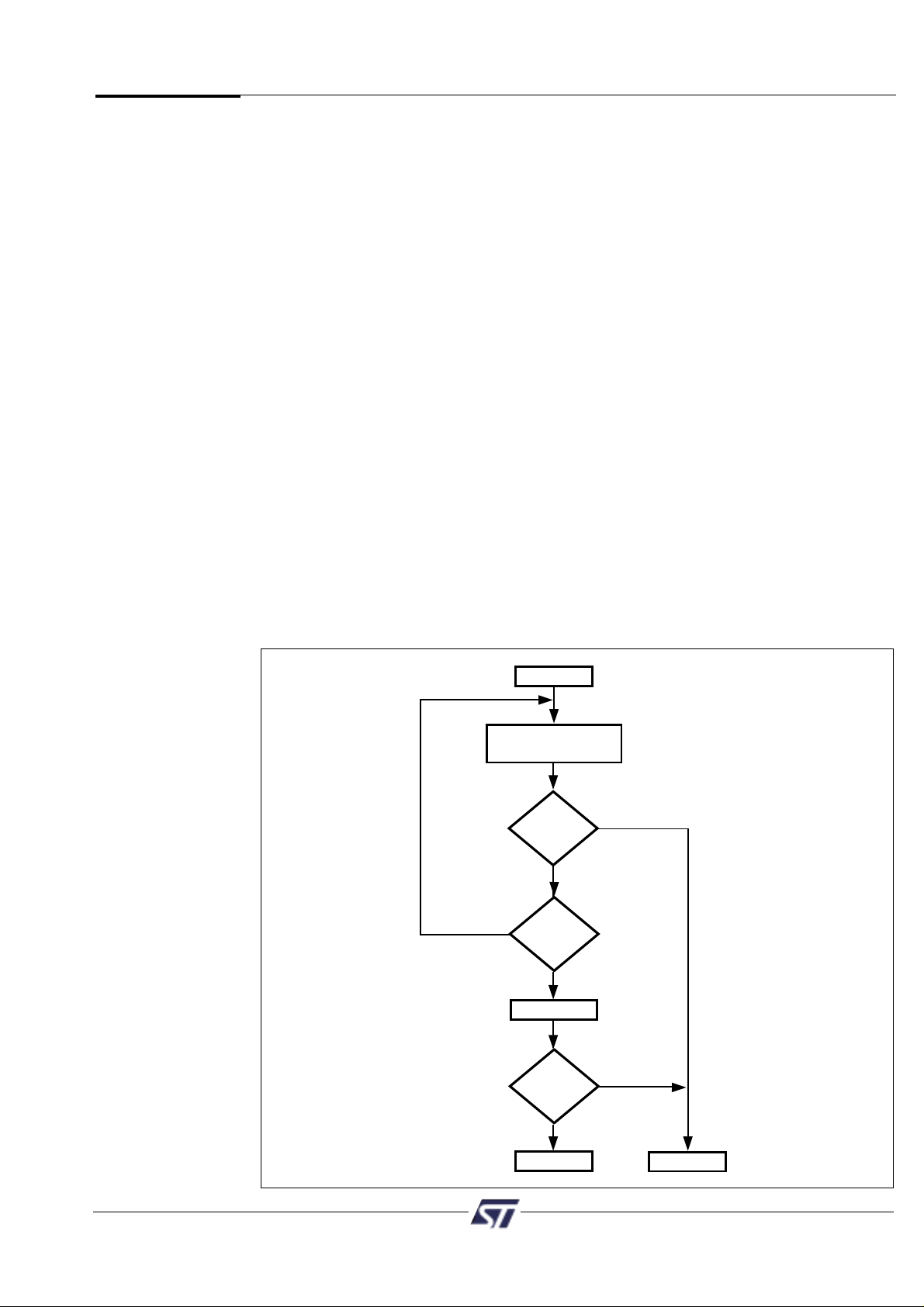
9.1.1.6.3 EEPROM Software Data Protect (SDP)
The SDP feature is useful for protecting the contents of EEPROM from inadvertent write
cycles that may occur during uncontrolled MCU bus conditions. These may happen if the
application software gets lost or when VCCis not within normal operating range.
Instructions from the MCU are used to enable and disable SDP mode (see Table 9). Once
enabled, the MCU must write an instruction sequence to EEPROM before writing data
(much like writing to Flash memory). SDP mode can be used for both byte and page writes
to EEPROM. The device will remain in SDP mode until the MCU issues a valid SDP disable
instruction.
PSD813F1 devices are shipped with SDP mode disabled. However, within PSDsoft, SDP
mode may be enabled as part of programming the device with a device programmer
(PSDpro).
The
PSD813F1
Functional
Blocks
(cont.)
Preliminary PSD813F1-A
23
WRITE AAh to
Address 555h
WRITE 55h to
Address AAAh
WRITE A0h to
Address 555h
Page Write
Instruction
SDP is set
WRITE AAh to
Address 555h
WRITE 55h to
Address AAAh
WRITE A0h to
Address 555h
WRITE Data to
be Written in
any Address
Page Write
Instruction
SDP
Set
SDP
not Set
Write
in Memory
Write Data
+
SDP Set
after tWC
(Write Cycle Time)
WRITE
is enabled
SDP ENABLE ALGORITHM
Figure 3. EEPROM SDP Enable Flowcharts
The
PSD813F1
Functional
Blocks
(cont.)
9.1.1.6.3 EEPROM Software Data Protect (SDP) (cont.)
To enable SDP mode at run time, the MCU must write three specific data bytes at three
specific memory locations, as shown in Figure 3. Any further writes to EEPROM when SDP
is set will require this same sequence, followed by the byte(s) to write. The first SDP enable
sequence can be followed directly by the byte(s) to be written.
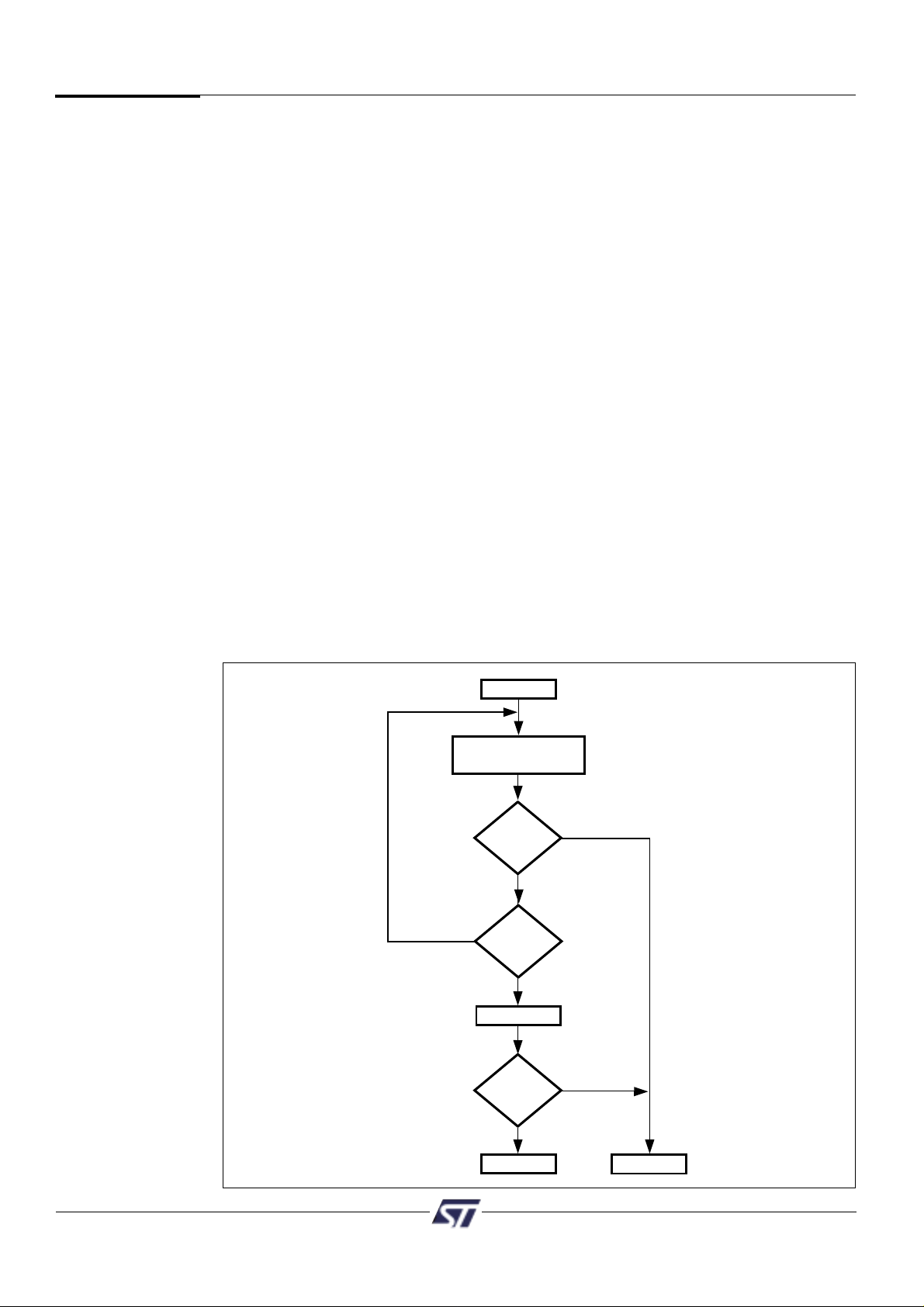
To disable SDP mode, the MCU must write specific bytes to six specific locations, as shown
in Figure 4.
The MCU must not be executing code from EEPROM when these instructions are invoked.
The MCU must be operating from some other memory when enabling or disabling SDP
mode.
The state of SDP mode is not changed by power on/off sequences (nonvolatile). When
either the SDP enable or SDP disable instructions are issued from the MCU, the MCU must
use the Toggle bit (status bit DQ6) or the Ready/Busy output pin to check programming
status. The Ready/Busy output is driven low from the first write of AAh @ 555h until the
completion of the internal storage sequence. Data Polling (status bit DQ7) is not supported
when issuing the SDP enable or SDP disable commands.
Note: Using the SDP sequence (enabling, disabling, or writing data) is initiated when
specific bytes are written to addresses on specific “pages” of EEPROM memory, with no
more than 120 µsec between writes. The addresses 555h and AAAh are located on
different pages of EEPROM. This is how the PSD813F1 distinguishes these instruction
sequences from ordinary writes to EEPROM, which are expected to be within a single
EEPROM page.
PSD813F1-A Preliminary
24
Figure 4. Software Data Protection Disable Flow Chart
9.1.1.6.4 Write OTP Row
Writing to the OTP row (64 bytes) can only be done once per byte, and is enabled by an
instruction. This instruction is composed of three specific Write operations of data bytes at
three specific memory locations followed by the data to be stored in the OTP row (refer to
Table 9). During the write operations, address bit A6 must be zero, while address bits A5-A0
define the OTP Row byte to be written while any EEPROM Sector Select signal (EESi) is
active. Writing the OTP Row is allowed only when SDP mode is not enabled.
9.1.1.7 Programming Flash Memory
Flash memory must be erased prior to being programmed. The MCU may erase Flash
memory all at once or by-sector, but not byte-by-byte. A byte of Flash memory erases to all
logic ones (FF hex), and its bits are programmed to logic zeros. Although erasing Flash
memory occurs on a sector basis, programming Flash memory occurs on a byte basis.
The PSD813F1 main Flash and optional boot Flash require the MCU to send an instruction
to program a byte or perform an erase function (see Table 9). This differs from EEPROM,
which can be programmed with simple MCU bus write operations (unless EEPROM SDP
mode is enabled).
Once the MCU issues a Flash memory program or erase instruction, it must check for the
status of completion. The embedded algorithms that are invoked inside the PSD813F1
support several means to provide status to the MCU. Status may be checked using any of
three methods: Data Polling, Data Toggle, or the Ready/Busy output pin.
WRITE AAh to
Address 555h
WRITE 55h to
Address AAAh
WRITE 80h to
Address 555h
WRITE AAh to
Address 555h
WRITE 55h to
Address AAAh
WRITE 20h to
Address 555h
Page Write
Instruction
Unprotected State
after
tWC (Write Cycle time)
The
PSD813F1
Functional
Blocks
(cont.)
Preliminary PSD813F1-A
25
The
PSD813F1
Functional
Blocks
(cont.)
9.1.1.7.1 Data Polling
Polling on DQ7 is a method of checking whether a Program or Erase instruction is in
progress or has completed. Figure 5 shows the Data Polling algorithm.
When the MCU issues a programming instruction, the embedded algorithm within the
PSD813F1 begins. The MCU then reads the location of the byte to be programmed in Flash
to check status. Data bit DQ7 of this location becomes the compliment of data bit 7of the
original data byte to be programmed. The MCU continues to poll this location, comparing
DQ7 and monitoring the Error bit on DQ5. When the DQ7 matches data bit 7 of the original
data, and the Error bit at DQ5 remains ‘0’, then the embedded algorithm is complete.
If the Error bit at DQ5 is ‘1’, the MCU should test DQ7 again since DQ7 may have changed
simultaneously with DQ5 (see Figure 5).
The Error bit at DQ5 will be set if either an internal timeout occurred while the embedded
algorithm attempted to program the byte or if the MCU attempted to program a ‘1’ to a bit
that was not erased (not erased is logic ‘0’).
It is suggested (as with all Flash memories) to read the location again after the embedded
programming algorithm has completed to compare the byte that was written to Flash with
the byte that was intended to be written.
When using the Data Polling method after an erase instruction, Figure 5 still applies.
However, DQ7 will be ‘0’ until the erase operation is complete. A ‘1’ on DQ5 will indicate
a timeout failure of the erase operation, a ‘0’ indicates no error. The MCU can read any
location within the sector being erased to get DQ7 and DQ5.
PSDsoft will generate ANSI C code functions which implement these Data Polling
algorithms.
Figure 5. Data Polling Flow Chart
START
READ DQ5 & DQ7
at VALID ADDRESS
YES
YES
YES
NO
NO
NO
DQ7
=
DATA7
DQ5
=1
DQ7
=
DATA
READ DQ7
FAIL PASS
PSD813F1-A Preliminary
26
9.1.1.7.2 Data Toggle
Checking the Data Toggle bit on DQ6 is a method of determining whether a Program or
Erase instruction is in progress or has completed. Figure 6 shows the Data Toggle
algorithm.
When the MCU issues a programming instruction, the embedded algorithm within the
PSD813F1 begins. The MCU then reads the location of the byte to be programmed in
Flash to check status. Data bit DQ6 of this location will toggle each time the MCU reads
this location until the embedded algorithm is complete. The MCU continues to read this
location, checking DQ6 and monitoring the Error bit on DQ5. When DQ6 stops toggling
(two consecutive reads yield the same value), and the Error bit on DQ5 remains ‘0’, then
the embedded algorithm is complete. If the Error bit on DQ5 is ‘1’, the MCU should test
DQ6 again, since DQ6 may have changed simultaneously with DQ5 (see Figure 6).
The Error bit at DQ5 will be set if either an internal timeout occurred while the embedded
algorithm attempted to program the byte, or if the MCU attempted to program a ‘1’ to a bit
that was not erased (not erased is logic ‘0’).
It is suggested (as with all Flash memories) to read the location again after the embedded
programming algorithm has completed to compare the byte that was written to Flash with
the byte that was intended to be written.
When using the Data Toggle method after an erase instructin, Figure 6 still applies. DQ6 will
toggle until the erase operation is complete. A ‘1’ on DQ5 will indicate a timeout failure of
the erase operation, a ‘0’ indicates no error. The MCU can read any location within the
sector being erased to get DQ6 and DQ5.
PSDsoft will generate ANSI C code functions which implement these Data Toggling
algorithms.
The
PSD813F1
Functional
Blocks
(cont.)
Figure 6. Data Toggle Flow Chart
START
READ
DQ5 & DQ6
NO
YES
NO
YES
YES
NO
DQ6
=
TOGGLE
DQ5
=1
DQ6
=
TOGGLE
READ DQ6
FAIL PASS
 Loading...