

SGS Thomson Microelectronics PSD4256G6V Datasheet
Flash In-System Programmable (ISP)
FEATURES SUMMARY
PSD provides an integrated solution to 16-bit
MCU-based applications that includes configurable memories, PLD logic, and I/O:
■ Dual bank Flash memories
– 8Mbits of Primary Flash Memory (16 uniform
sectors, 64Kbyte)
– 512Kbits of Seconda ry Flash M emory wi th 4
sectors
– Concurrent operation: READ from one mem-
ory while erasing and writing the other
■ 256Kbits of SRAM (battery-backed)
■ PLD with Macrocells
– Over 3000 Gates of PLD: CPLD and DPLD
– CPLD with 16 Output Macrocells (OMCs) and
24 Input Macrocells (IMCs)
– DPLD - user def ined internal chip sel ect de-
coding
■ Seven l/O Ports with 52 I/O pins:
52 individually configurable I/O port pins that
can be used for the following functions:
– MCU I/Os
–PLD I/Os
– Latched MCU address output
– Special function I/Os
– l/O ports may be configured as open-drain
outputs
■ In-System Programming (ISP) with JTAG
– Built-in JTAG compliant serial port allows full-
chip In-System Programmability
– Efficient manufacturing allow easy product
testing and programming
– Use low cost FlashLINK cable with PC
■ Page Register
– Internal page register that can be used to ex-
pand the microcontroller address space by a
factor of 256
■ Programmable power management
PSD4256G6V
Peripherals for 16-bit MCUs
PRELIMINARY DATA
■ High Endurance:
– 100,000 Erase/WRITE Cycles of Flash Mem-
ory
– 1,000 Erase/WRITE Cycles of PLD
– 15 Year Data Retention
■ Single Supply Voltage
– 3V (+20%/–10%)
■ Memory Speed
– 100ns Flash memory and SRAM access time
for V
– 90ns Flash memory and SRAM access t ime
for V
Figure 1. 80-lead, Thin, Quad, Flat Package
= 3V (+20%/–10%)
CC
= 3.3V (+/–10%)
CC
TQFP80 (U)
December 2002
This is preliminary information on a new product now in development or undergoing evaluation. Details are subject to change without notice.
1/100

PSD4256G6V
TABLE OF CONTENTS
SUMMARY DESCRIPTION. . . . . . . . . . . . . . . . . . . . . . . . . . . . . . . . . . . . . . . . . . . . . . . . . . . . . . . . . . . 9
In-System Programming (ISP) via JTAG. . . . . . . . . . . . . . . . . . . . . . . . . . . . . . . . . . . . . . . . . . . . . . 9
PSDsoft . . . . . . . . . . . . . . . . . . . . . . . . . . . . . . . . . . . . . . . . . . . . . . . . . . . . . . . . . . . . . . . . . . . . . . . 9
Logic Diagram (Figu re 2.) . . . . . . . . . . . . . . . . . . . . . . . . . . . . . . . . . . . . . . . . . . . . . . . . . . . . . . . . 10
Pin Names (Table 1.). . . . . . . . . . . . . . . . . . . . . . . . . . . . . . . . . . . . . . . . . . . . . . . . . . . . . . . . . . . . 10
TQFP80 Connections (Figure 3.) . . . . . . . . . . . . . . . . . . . . . . . . . . . . . . . . . . . . . . . . . . . . . . . . . . 11
TQFP80 Pin Descripti o n (Table 2. ). . . . . . . . . . . . . . . . . . . . . . . . . . . . . . . . . . . . . . . . . . . . . . . . . 12
PSD Block Diagram (Figure 4.). . . . . . . . . . . . . . . . . . . . . . . . . . . . . . . . . . . . . . . . . . . . . . . . . . . . 15
PSD ARCHITECTURAL OVERVIEW . . . . . . . . . . . . . . . . . . . . . . . . . . . . . . . . . . . . . . . . . . . . . . . . . . 16
Memory . . . . . . . . . . . . . . . . . . . . . . . . . . . . . . . . . . . . . . . . . . . . . . . . . . . . . . . . . . . . . . . . . . . . . . 16
PLDs . . . . . . . . . . . . . . . . . . . . . . . . . . . . . . . . . . . . . . . . . . . . . . . . . . . . . . . . . . . . . . . . . . . . . . . . 16
I/O Ports . . . . . . . . . . . . . . . . . . . . . . . . . . . . . . . . . . . . . . . . . . . . . . . . . . . . . . . . . . . . . . . . . . . . . 16
MCU Bus Interface . . . . . . . . . . . . . . . . . . . . . . . . . . . . . . . . . . . . . . . . . . . . . . . . . . . . . . . . . . . . . 16
ISP via JTAG Port . . . . . . . . . . . . . . . . . . . . . . . . . . . . . . . . . . . . . . . . . . . . . . . . . . . . . . . . . . . . . . 16
PLD I/O (Table 3.). . . . . . . . . . . . . . . . . . . . . . . . . . . . . . . . . . . . . . . . . . . . . . . . . . . . . . . . . . . . . . 16
JTAG Signals on Port E (Table 4.) . . . . . . . . . . . . . . . . . . . . . . . . . . . . . . . . . . . . . . . . . . . . . . . . . 16
In-System Programming (ISP). . . . . . . . . . . . . . . . . . . . . . . . . . . . . . . . . . . . . . . . . . . . . . . . . . . . . 17
In-Application Programming (IAP). . . . . . . . . . . . . . . . . . . . . . . . . . . . . . . . . . . . . . . . . . . . . . . . . . 17
Page Register . . . . . . . . . . . . . . . . . . . . . . . . . . . . . . . . . . . . . . . . . . . . . . . . . . . . . . . . . . . . . . . . . 17
Methods of Programming Different Functional Blocks of the PSD (Table 5.) . . . . . . . . . . . . . . . . . 17
DEVELOPMENT SYSTEM . . . . . . . . . . . . . . . . . . . . . . . . . . . . . . . . . . . . . . . . . . . . . . . . . . . . . . . . . . 18
PSDsoft Development Tool (Figure 5.) . . . . . . . . . . . . . . . . . . . . . . . . . . . . . . . . . . . . . . . . . . . . . .18
PSD REGISTER DESCRIPTION AND ADDRESS OFFSETS . . . . . . . . . . . . . . . . . . . . . . . . . . . . . . . 19
Register Address Of fse t (Table 6.) . . . . . . . . . . . . . . . . . . . . . . . . . . . . . . . . . . . . . . . . . . . . . . . . . 19
REGISTER BIT DEFINITI ON . . . . . . . . . . . . . . . . . . . . . . . . . . . . . . . . . . . . . . . . . . . . . . . . . . . . . . . . 20
Data-In Registers - Ports A, B, C, D, E, F, and G (Table 7.). . . . . . . . . . . . . . . . . . . . . . . . . . . . . . 20
Data-Out Registers - Ports A, B, C, D, E, F, and G (Table 8.) . . . . . . . . . . . . . . . . . . . . . . . . . . . . 20
Direction Registers - Ports A, B, C, D, E, F, and G (Table 9.). . . . . . . . . . . . . . . . . . . . . . . . . . . . . 20
Control Registe r s - Ports E, F, and G (Table 10.) . . . . . . . . . . . . . . . . . . . . . . . . . . . . . . . . . . . . . . 20
Drive Registers - Ports A, B, D, E, and G (Table 11.) . . . . . . . . . . . . . . . . . . . . . . . . . . . . . . . . . . . 20
Enable-Out Registe r s - Ports A, B, C, and F (Table 12.). . . . . . . . . . . . . . . . . . . . . . . . . . . . . . . . . 20
Input Macrocells - Por ts A, B, a nd C (Table 13.). . . . . . . . . . . . . . . . . . . . . . . . . . . . . . . . . . . . . . . 21
Output Macrocell s A Regis te r (Tab le 14.) . . . . . . . . . . . . . . . . . . . . . . . . . . . . . . . . . . . . . . . . . . . . 21
Out Macrocells B Regist e r (Ta b le 1 5.) . . . . . . . . . . . . . . . . . . . . . . . . . . . . . . . . . . . . . . . . . . . . . .21
Mask Macrocells A Register (Table 16.) . . . . . . . . . . . . . . . . . . . . . . . . . . . . . . . . . . . . . . . . . . . . .21
Mask Macrocells B Register (Table 17.) . . . . . . . . . . . . . . . . . . . . . . . . . . . . . . . . . . . . . . . . . . . . .21
2/100
This is preliminary information on a new product now in development or undergoing evaluation. Details are subject to change without notice.

PSD4256G6V
Flash Memory Protection Register 1 (Table 18.). . . . . . . . . . . . . . . . . . . . . . . . . . . . . . . . . . . . . . .21
Flash Memory Protections Register 2 (Table 19.). . . . . . . . . . . . . . . . . . . . . . . . . . . . . . . . . . . . . .21
Flash Boot Protec tion Register (Table 20.) . . . . . . . . . . . . . . . . . . . . . . . . . . . . . . . . . . . . . . . . . . .22
JTAG Enable Register (Table 21.) . . . . . . . . . . . . . . . . . . . . . . . . . . . . . . . . . . . . . . . . . . . . . . . . . 22
Page Register (Table 22. ). . . . . . . . . . . . . . . . . . . . . . . . . . . . . . . . . . . . . . . . . . . . . . . . . . . . . . . . 22
PMMR0 Register (Table 23.). . . . . . . . . . . . . . . . . . . . . . . . . . . . . . . . . . . . . . . . . . . . . . . . . . . . . . 23
PMMR2 Register (Table 24.). . . . . . . . . . . . . . . . . . . . . . . . . . . . . . . . . . . . . . . . . . . . . . . . . . . . . . 23
VM Register (Table 25.) . . . . . . . . . . . . . . . . . . . . . . . . . . . . . . . . . . . . . . . . . . . . . . . . . . . . . . . . . 23
Memory_ID0 Register (Table 26.). . . . . . . . . . . . . . . . . . . . . . . . . . . . . . . . . . . . . . . . . . . . . . . . . . 24
Memory_ID1 Register (Table 27.). . . . . . . . . . . . . . . . . . . . . . . . . . . . . . . . . . . . . . . . . . . . . . . . . . 24
DETAILED OPERATION. . . . . . . . . . . . . . . . . . . . . . . . . . . . . . . . . . . . . . . . . . . . . . . . . . . . . . . . . . . . 25
Memory Blocks . . . . . . . . . . . . . . . . . . . . . . . . . . . . . . . . . . . . . . . . . . . . . . . . . . . . . . . . . . . . . . . . 25
Memory Block Size and Organization (Table 28.). . . . . . . . . . . . . . . . . . . . . . . . . . . . . . . . . . . . . . 25
Primary Flash Memory and Secondary Flash m emo ry Description. . . . . . . . . . . . . . . . . . . . . . . . . 26
Ready/Busy (PE4). . . . . . . . . . . . . . . . . . . . . . . . . . . . . . . . . . . . . . . . . . . . . . . . . . . . . . . . . . . . . . 26
Memory Operation. . . . . . . . . . . . . . . . . . . . . . . . . . . . . . . . . . . . . . . . . . . . . . . . . . . . . . . . . . . . . . 26
16-bit Instructions (Table 29.) . . . . . . . . . . . . . . . . . . . . . . . . . . . . . . . . . . . . . . . . . . . . . . . . . . . . . 27
INSTRUCTIONS . . . . . . . . . . . . . . . . . . . . . . . . . . . . . . . . . . . . . . . . . . . . . . . . . . . . . . . . . . . . . . . . . . 28
Power-up Conditio n. . . . . . . . . . . . . . . . . . . . . . . . . . . . . . . . . . . . . . . . . . . . . . . . . . . . . . . . . . . . . 28
READ. . . . . . . . . . . . . . . . . . . . . . . . . . . . . . . . . . . . . . . . . . . . . . . . . . . . . . . . . . . . . . . . . . . . . . . . 28
READ Memory Contents. . . . . . . . . . . . . . . . . . . . . . . . . . . . . . . . . . . . . . . . . . . . . . . . . . . . . . . . . 28
READ Primary Flash Identifier . . . . . . . . . . . . . . . . . . . . . . . . . . . . . . . . . . . . . . . . . . . . . . . . . . . . . 2 8
READ Memory Sector Protection Status . . . . . . . . . . . . . . . . . . . . . . . . . . . . . . . . . . . . . . . . . . . . . 28
Reading the Erase/Program Status Bits . . . . . . . . . . . . . . . . . . . . . . . . . . . . . . . . . . . . . . . . . . . . . 29
Status Bits (Table 30.). . . . . . . . . . . . . . . . . . . . . . . . . . . . . . . . . . . . . . . . . . . . . . . . . . . . . . . . . . . 29
Status Bits for Motoro la 16-bit MCU (Table 31.) . . . . . . . . . . . . . . . . . . . . . . . . . . . . . . . . . . . . . . . 29
Data Polling (DQ7) - DQ15 for Motorola . . . . . . . . . . . . . . . . . . . . . . . . . . . . . . . . . . . . . . . . . . . . .30
Toggle Flag (DQ6) – DQ14 for Motorola . . . . . . . . . . . . . . . . . . . . . . . . . . . . . . . . . . . . . . . . . . . . . 30
Error Flag (DQ5) – DQ13 for Motorola . . . . . . . . . . . . . . . . . . . . . . . . . . . . . . . . . . . . . . . . . . . . . .30
Erase Time-out Flag (DQ3) – DQ11 for Motorola . . . . . . . . . . . . . . . . . . . . . . . . . . . . . . . . . . . . . . 30
PROGRAMMING FLASH MEMORY . . . . . . . . . . . . . . . . . . . . . . . . . . . . . . . . . . . . . . . . . . . . . . . . . . . 31
Data Polling. . . . . . . . . . . . . . . . . . . . . . . . . . . . . . . . . . . . . . . . . . . . . . . . . . . . . . . . . . . . . . . . . . . 3 1
Data Polling Flowchart (Figure 6.). . . . . . . . . . . . . . . . . . . . . . . . . . . . . . . . . . . . . . . . . . . . . . . . . . 31
Data Toggle . . . . . . . . . . . . . . . . . . . . . . . . . . . . . . . . . . . . . . . . . . . . . . . . . . . . . . . . . . . . . . . . . . . 32
Unlock Bypass. . . . . . . . . . . . . . . . . . . . . . . . . . . . . . . . . . . . . . . . . . . . . . . . . . . . . . . . . . . . . . . . . 32
Data Toggle Flowchart (Figure 7.) . . . . . . . . . . . . . . . . . . . . . . . . . . . . . . . . . . . . . . . . . . . . . . . . . . 32
3/100
This is preliminary information on a new product now in development or undergoing evaluation. Details are subject to change without notice.

PSD4256G6V
ERASING FLASH MEMORY . . . . . . . . . . . . . . . . . . . . . . . . . . . . . . . . . . . . . . . . . . . . . . . . . . . . . . . . 33
Flash Bulk Erase . . . . . . . . . . . . . . . . . . . . . . . . . . . . . . . . . . . . . . . . . . . . . . . . . . . . . . . . . . . . . . . 33
Flash Sector Erase . . . . . . . . . . . . . . . . . . . . . . . . . . . . . . . . . . . . . . . . . . . . . . . . . . . . . . . . . . . . . 33
Suspend Sector Erase. . . . . . . . . . . . . . . . . . . . . . . . . . . . . . . . . . . . . . . . . . . . . . . . . . . . . . . . . . . 33
Resume Sector Erase . . . . . . . . . . . . . . . . . . . . . . . . . . . . . . . . . . . . . . . . . . . . . . . . . . . . . . . . . . . 33
SPECIFIC FEATURES . . . . . . . . . . . . . . . . . . . . . . . . . . . . . . . . . . . . . . . . . . . . . . . . . . . . . . . . . . . . . 34
Flash Memory Sector Protect . . . . . . . . . . . . . . . . . . . . . . . . . . . . . . . . . . . . . . . . . . . . . . . . . . . . . 34
RESET. . . . . . . . . . . . . . . . . . . . . . . . . . . . . . . . . . . . . . . . . . . . . . . . . . . . . . . . . . . . . . . . . . . . . . . 34
Reset (RESET) Pin . . . . . . . . . . . . . . . . . . . . . . . . . . . . . . . . . . . . . . . . . . . . . . . . . . . . . . . . . . . . . 34
SRAM . . . . . . . . . . . . . . . . . . . . . . . . . . . . . . . . . . . . . . . . . . . . . . . . . . . . . . . . . . . . . . . . . . . . . . . . . . 34
MEMORY SELECT SIGNALS. . . . . . . . . . . . . . . . . . . . . . . . . . . . . . . . . . . . . . . . . . . . . . . . . . . . . . . . 35
Example. . . . . . . . . . . . . . . . . . . . . . . . . . . . . . . . . . . . . . . . . . . . . . . . . . . . . . . . . . . . . . . . . . . . . . 35
Priority Level of Memory and I/O Components (Figure 8.) . . . . . . . . . . . . . . . . . . . . . . . . . . . . . . . 35
Configuration Modes for MCUs with Separate Program and Data Spaces. . . . . . . . . . . . . . . . . . . 36
Combined Space Mode s . . . . . . . . . . . . . . . . . . . . . . . . . . . . . . . . . . . . . . . . . . . . . . . . . . . . . . . . . 36
80C31 Memory Map Example. . . . . . . . . . . . . . . . . . . . . . . . . . . . . . . . . . . . . . . . . . . . . . . . . . . . .36
8031 Memory Modules – Separate Space (Figure 9.). . . . . . . . . . . . . . . . . . . . . . . . . . . . . . . . . . . 36
8031 Memory Modules – Combined Space (Figure 10.). . . . . . . . . . . . . . . . . . . . . . . . . . . . . . . . . 36
PAGE REGISTER . . . . . . . . . . . . . . . . . . . . . . . . . . . . . . . . . . . . . . . . . . . . . . . . . . . . . . . . . . . . . . . . . 37
Page Register (Figure 11.) . . . . . . . . . . . . . . . . . . . . . . . . . . . . . . . . . . . . . . . . . . . . . . . . . . . . . . . 37
MEMORY ID REGISTERS . . . . . . . . . . . . . . . . . . . . . . . . . . . . . . . . . . . . . . . . . . . . . . . . . . . . . . . . . . 37
PLDs . . . . . . . . . . . . . . . . . . . . . . . . . . . . . . . . . . . . . . . . . . . . . . . . . . . . . . . . . . . . . . . . . . . . . . . . . . . 38
The Turbo Bit in PSD. . . . . . . . . . . . . . . . . . . . . . . . . . . . . . . . . . . . . . . . . . . . . . . . . . . . . . . . . . . . 38
DPLD and CPLD Inputs (Table 32.) . . . . . . . . . . . . . . . . . . . . . . . . . . . . . . . . . . . . . . . . . . . . . . . .38
PLD Diagram (Figure 12.). . . . . . . . . . . . . . . . . . . . . . . . . . . . . . . . . . . . . . . . . . . . . . . . . . . . . . . . 39
DECODE PLD (DPLD) . . . . . . . . . . . . . . . . . . . . . . . . . . . . . . . . . . . . . . . . . . . . . . . . . . . . . . . . . . . . . 40
DPLD Logic Array (Figure 13.) . . . . . . . . . . . . . . . . . . . . . . . . . . . . . . . . . . . . . . . . . . . . . . . . . . . . 40
COMPLEX PLD (CPLD) . . . . . . . . . . . . . . . . . . . . . . . . . . . . . . . . . . . . . . . . . . . . . . . . . . . . . . . . . . . . 41
Macrocell and I/O Port (Figure 14.). . . . . . . . . . . . . . . . . . . . . . . . . . . . . . . . . . . . . . . . . . . . . . . . . 41
Output Macrocell (OMC) . . . . . . . . . . . . . . . . . . . . . . . . . . . . . . . . . . . . . . . . . . . . . . . . . . . . . . . . . 42
Output Macrocell Port and Data Bit Assignments (Table 33.). . . . . . . . . . . . . . . . . . . . . . . . . . . . . 42
Product Term Allocator . . . . . . . . . . . . . . . . . . . . . . . . . . . . . . . . . . . . . . . . . . . . . . . . . . . . . . . . . . 43
4/100
This is preliminary information on a new product now in development or undergoing evaluation. Details are subject to change without notice.

PSD4256G6V
Loading and Reading the Output Macrocells (OM C). . . . . . . . . . . . . . . . . . . . . . . . . . . . . . . . . . . . 43
The OMC Mask Register. . . . . . . . . . . . . . . . . . . . . . . . . . . . . . . . . . . . . . . . . . . . . . . . . . . . . . . . . 43
The Output Enable of the OMC. . . . . . . . . . . . . . . . . . . . . . . . . . . . . . . . . . . . . . . . . . . . . . . . . . . . 43
CPLD Output Macrocell (Figure 15.). . . . . . . . . . . . . . . . . . . . . . . . . . . . . . . . . . . . . . . . . . . . . . . .44
Input Macrocells (IMC) . . . . . . . . . . . . . . . . . . . . . . . . . . . . . . . . . . . . . . . . . . . . . . . . . . . . . . . . . . 45
Input Macrocell (Figure 16.). . . . . . . . . . . . . . . . . . . . . . . . . . . . . . . . . . . . . . . . . . . . . . . . . . . . . . . 45
External Chip Select . . . . . . . . . . . . . . . . . . . . . . . . . . . . . . . . . . . . . . . . . . . . . . . . . . . . . . . . . . . . 46
External Chip Select Signal (Figure 17.). . . . . . . . . . . . . . . . . . . . . . . . . . . . . . . . . . . . . . . . . . . . .46
Handshaking Communication Using Input Macrocells (Figure 18.). . . . . . . . . . . . . . . . . . . . . . . . . 46
MCU BUS INTERFACE. . . . . . . . . . . . . . . . . . . . . . . . . . . . . . . . . . . . . . . . . . . . . . . . . . . . . . . . . . . . . 47
16-bit MCUs and Their Control Signals (Table 34.). . . . . . . . . . . . . . . . . . . . . . . . . . . . . . . . . . . . . 47
PSD Interface to a Multiplexed Bus . . . . . . . . . . . . . . . . . . . . . . . . . . . . . . . . . . . . . . . . . . . . . . . . . 48
An Example of a Typical Multi plexed Bus Interface (Figure 19.). . . . . . . . . . . . . . . . . . . . . . . . . . . 48
PSD Interface to a Non-Multiplexed, 16-bit Bus . . . . . . . . . . . . . . . . . . . . . . . . . . . . . . . . . . . . . . . 49
An Example of a Typical Non-Multiplexed Bus Interface (Figure 20.). . . . . . . . . . . . . . . . . . . . . . . 49
Data Byte Enable Reference for a 16-bit Bus . . . . . . . . . . . . . . . . . . . . . . . . . . . . . . . . . . . . . . . . .50
16-Bit Data Bus with BHE (Table 35.). . . . . . . . . . . . . . . . . . . . . . . . . . . . . . . . . . . . . . . . . . . . . . .50
16-bit MCU Bus Interface Exa mpl es. . . . . . . . . . . . . . . . . . . . . . . . . . . . . . . . . . . . . . . . . . . . . . . .50
16-Bit Data Bus with WRH and WRL (Table 36.) . . . . . . . . . . . . . . . . . . . . . . . . . . . . . . . . . . . . . . 50
16-Bit Data Bus with SIZ0, A0 (Mot o r ola MCU) (Tab le 3 7. ) . . . . . . . . . . . . . . . . . . . . . . . . . . . . . . 50
16-Bit Data Bus with LDS, UDS (Moto r o la MCU) (Tab le 3 8. ). . . . . . . . . . . . . . . . . . . . . . . . . . . . . 50
80C196 and 80C186 . . . . . . . . . . . . . . . . . . . . . . . . . . . . . . . . . . . . . . . . . . . . . . . . . . . . . . . . . . . . 51
Interfacing the PSD with an 80C196 (Figure 21.) . . . . . . . . . . . . . . . . . . . . . . . . . . . . . . . . . . . . . . 51
MC683xx and MC68HC16. . . . . . . . . . . . . . . . . . . . . . . . . . . . . . . . . . . . . . . . . . . . . . . . . . . . . . . . 52
Interfacing the PSD with an MC68331 (Figure 22.). . . . . . . . . . . . . . . . . . . . . . . . . . . . . . . . . . . . . 52
80C51XA. . . . . . . . . . . . . . . . . . . . . . . . . . . . . . . . . . . . . . . . . . . . . . . . . . . . . . . . . . . . . . . . . . . . . 53
Interfacing the PSD with an 80C51XA-G3 (Figure 23.). . . . . . . . . . . . . . . . . . . . . . . . . . . . . . . . . . 53
H8/300. . . . . . . . . . . . . . . . . . . . . . . . . . . . . . . . . . . . . . . . . . . . . . . . . . . . . . . . . . . . . . . . . . . . . . . 54
Interfacing the PSD with an H83/2350 (Figure 24.). . . . . . . . . . . . . . . . . . . . . . . . . . . . . . . . . . . . . 54
MMC2001 . . . . . . . . . . . . . . . . . . . . . . . . . . . . . . . . . . . . . . . . . . . . . . . . . . . . . . . . . . . . . . . . . . . . 55
C16x Family. . . . . . . . . . . . . . . . . . . . . . . . . . . . . . . . . . . . . . . . . . . . . . . . . . . . . . . . . . . . . . . . . . . 55
Interfacing the PSD with an MMC2001 (Figure 25.) . . . . . . . . . . . . . . . . . . . . . . . . . . . . . . . . . . . . 56
Interfacing the PSD with a C167CR (Figure 26.). . . . . . . . . . . . . . . . . . . . . . . . . . . . . . . . . . . . . . . 57
I/O PORTS. . . . . . . . . . . . . . . . . . . . . . . . . . . . . . . . . . . . . . . . . . . . . . . . . . . . . . . . . . . . . . . . . . . . . . . 58
General Port Architecture . . . . . . . . . . . . . . . . . . . . . . . . . . . . . . . . . . . . . . . . . . . . . . . . . . . . . . . . 58
Port Operating Modes . . . . . . . . . . . . . . . . . . . . . . . . . . . . . . . . . . . . . . . . . . . . . . . . . . . . . . . . . . . 58
General I/O Port Architecture (Figure 27.). . . . . . . . . . . . . . . . . . . . . . . . . . . . . . . . . . . . . . . . . . . .59
MCU I/O Mode. . . . . . . . . . . . . . . . . . . . . . . . . . . . . . . . . . . . . . . . . . . . . . . . . . . . . . . . . . . . . . . . . 60
PLD I/O Mode . . . . . . . . . . . . . . . . . . . . . . . . . . . . . . . . . . . . . . . . . . . . . . . . . . . . . . . . . . . . . . . . . 60
Address Out Mode. . . . . . . . . . . . . . . . . . . . . . . . . . . . . . . . . . . . . . . . . . . . . . . . . . . . . . . . . . . . . . 60
Port Operating Modes (Table 39.). . . . . . . . . . . . . . . . . . . . . . . . . . . . . . . . . . . . . . . . . . . . . . . . . . 60
Port Operating Mode Settings (Table 40.). . . . . . . . . . . . . . . . . . . . . . . . . . . . . . . . . . . . . . . . . . . . 61
I/O Port Latched Address Output Assignments (Table 41.) . . . . . . . . . . . . . . . . . . . . . . . . . . . . . . 61
Address In Mode . . . . . . . . . . . . . . . . . . . . . . . . . . . . . . . . . . . . . . . . . . . . . . . . . . . . . . . . . . . . . . . 62
5/100
This is preliminary information on a new product now in development or undergoing evaluation. Details are subject to change without notice.

PSD4256G6V
Data Port Mode . . . . . . . . . . . . . . . . . . . . . . . . . . . . . . . . . . . . . . . . . . . . . . . . . . . . . . . . . . . . . . . . 62
Peripheral I/O Mode . . . . . . . . . . . . . . . . . . . . . . . . . . . . . . . . . . . . . . . . . . . . . . . . . . . . . . . . . . . . 62
Peripheral I/O Mode (Figure 28.). . . . . . . . . . . . . . . . . . . . . . . . . . . . . . . . . . . . . . . . . . . . . . . . . . . 6 2
JTAG In-System Programming (ISP) . . . . . . . . . . . . . . . . . . . . . . . . . . . . . . . . . . . . . . . . . . . . . . . 63
MCU RESET Mode . . . . . . . . . . . . . . . . . . . . . . . . . . . . . . . . . . . . . . . . . . . . . . . . . . . . . . . . . . . . . 63
Port Configurati o n Regi ste rs ( PCR) . . . . . . . . . . . . . . . . . . . . . . . . . . . . . . . . . . . . . . . . . . . . . . . . 63
Control Registe r. . . . . . . . . . . . . . . . . . . . . . . . . . . . . . . . . . . . . . . . . . . . . . . . . . . . . . . . . . . . . . . . 63
Port Configurati o n Regi ste rs ( PCR) (Table 42.) . . . . . . . . . . . . . . . . . . . . . . . . . . . . . . . . . . . . . . . 63
Direction Register . . . . . . . . . . . . . . . . . . . . . . . . . . . . . . . . . . . . . . . . . . . . . . . . . . . . . . . . . . . . . . 64
Drive Select Register. . . . . . . . . . . . . . . . . . . . . . . . . . . . . . . . . . . . . . . . . . . . . . . . . . . . . . . . . . . . 64
Port Pin Direction Control, Output Enable P.T. Not Defined (Table 43.). . . . . . . . . . . . . . . . . . . . . 64
Port Pin Direction Control, Output Enable P.T. Defined (Table 44.) . . . . . . . . . . . . . . . . . . . . . . . . 64
Port Direction Assignment Example (Table 45.) . . . . . . . . . . . . . . . . . . . . . . . . . . . . . . . . . . . . . . .64
Drive Register Pin Assignment (Table 46.). . . . . . . . . . . . . . . . . . . . . . . . . . . . . . . . . . . . . . . . . . . 64
Port Data Registers. . . . . . . . . . . . . . . . . . . . . . . . . . . . . . . . . . . . . . . . . . . . . . . . . . . . . . . . . . . . . 65
Data In. . . . . . . . . . . . . . . . . . . . . . . . . . . . . . . . . . . . . . . . . . . . . . . . . . . . . . . . . . . . . . . . . . . . . . . 65
Data Out Register . . . . . . . . . . . . . . . . . . . . . . . . . . . . . . . . . . . . . . . . . . . . . . . . . . . . . . . . . . . . . .65
Output Macrocells (OMC) . . . . . . . . . . . . . . . . . . . . . . . . . . . . . . . . . . . . . . . . . . . . . . . . . . . . . . . . 65
Mask Macrocell Regist e r. . . . . . . . . . . . . . . . . . . . . . . . . . . . . . . . . . . . . . . . . . . . . . . . . . . . . . . . . 65
Input Macrocells (IMC) . . . . . . . . . . . . . . . . . . . . . . . . . . . . . . . . . . . . . . . . . . . . . . . . . . . . . . . . . . 65
Port Data Registers (Table 47.). . . . . . . . . . . . . . . . . . . . . . . . . . . . . . . . . . . . . . . . . . . . . . . . . . . . 65
Enable Out. . . . . . . . . . . . . . . . . . . . . . . . . . . . . . . . . . . . . . . . . . . . . . . . . . . . . . . . . . . . . . . . . . . . 66
Ports A, B and C – Functionality and Structure. . . . . . . . . . . . . . . . . . . . . . . . . . . . . . . . . . . . . . . . 66
Port A, B, and C Structure (Figure 29.). . . . . . . . . . . . . . . . . . . . . . . . . . . . . . . . . . . . . . . . . . . . . . 66
Port D – Functionality a n d Str uc tu r e . . . . . . . . . . . . . . . . . . . . . . . . . . . . . . . . . . . . . . . . . . . . . . . . 67
Port D Structure (Figure 30.). . . . . . . . . . . . . . . . . . . . . . . . . . . . . . . . . . . . . . . . . . . . . . . . . . . . . . 67
Port E – Functionality and Structure . . . . . . . . . . . . . . . . . . . . . . . . . . . . . . . . . . . . . . . . . . . . . . . . 68
Port F – Functionality and Structure . . . . . . . . . . . . . . . . . . . . . . . . . . . . . . . . . . . . . . . . . . . . . . . . 6 8
Port G – Functionality and Structure. . . . . . . . . . . . . . . . . . . . . . . . . . . . . . . . . . . . . . . . . . . . . . . . 68
Port E, F, and G Structure (Figure 31.) . . . . . . . . . . . . . . . . . . . . . . . . . . . . . . . . . . . . . . . . . . . . . . 69
6/100
This is preliminary information on a new product now in development or undergoing evaluation. Details are subject to change without notice.

PSD4256G6V
POWER MANAGEMENT . . . . . . . . . . . . . . . . . . . . . . . . . . . . . . . . . . . . . . . . . . . . . . . . . . . . . . . . . . . 70
Automatic Power-down (APD) Unit and Power-down Mode . . . . . . . . . . . . . . . . . . . . . . . . . . . . . . 71
Power-down Mode. . . . . . . . . . . . . . . . . . . . . . . . . . . . . . . . . . . . . . . . . . . . . . . . . . . . . . . . . . . . . . 71
Effect of Power-down Mode on Ports (Table 48.) . . . . . . . . . . . . . . . . . . . . . . . . . . . . . . . . . . . . . . 71
APD Unit (Figure 32.) . . . . . . . . . . . . . . . . . . . . . . . . . . . . . . . . . . . . . . . . . . . . . . . . . . . . . . . . . . . 71
PSD Timing and Standby Current During Power-down Mode (Table 49.) . . . . . . . . . . . . . . . . . . . 71
Other Power Saving Options. . . . . . . . . . . . . . . . . . . . . . . . . . . . . . . . . . . . . . . . . . . . . . . . . . . . . . 72
PLD Power Management . . . . . . . . . . . . . . . . . . . . . . . . . . . . . . . . . . . . . . . . . . . . . . . . . . . . . . . . 72
SRAM Standby Mode (Battery Backup) . . . . . . . . . . . . . . . . . . . . . . . . . . . . . . . . . . . . . . . . . . . . . 72
PSD Chip Select Input (CSI, PD2) . . . . . . . . . . . . . . . . . . . . . . . . . . . . . . . . . . . . . . . . . . . . . . . . . 72
Input Clock. . . . . . . . . . . . . . . . . . . . . . . . . . . . . . . . . . . . . . . . . . . . . . . . . . . . . . . . . . . . . . . . . . . . 72
Enable Power-down Fl ow Char t ( Fig u r e 33.) . . . . . . . . . . . . . . . . . . . . . . . . . . . . . . . . . . . . . . . . . 72
Input Contro l Signals. . . . . . . . . . . . . . . . . . . . . . . . . . . . . . . . . . . . . . . . . . . . . . . . . . . . . . . . . . . . 73
ADP Counter Operation (Table 50.) . . . . . . . . . . . . . . . . . . . . . . . . . . . . . . . . . . . . . . . . . . . . . . . .73
RESET TIMING AND DEVICE STATUS AT RESET . . . . . . . . . . . . . . . . . . . . . . . . . . . . . . . . . . . . . . 74
Power-on RESET . . . . . . . . . . . . . . . . . . . . . . . . . . . . . . . . . . . . . . . . . . . . . . . . . . . . . . . . . . . . . . 74
Warm RESET . . . . . . . . . . . . . . . . . . . . . . . . . . . . . . . . . . . . . . . . . . . . . . . . . . . . . . . . . . . . . . . . . 74
I/O Pin, Register and PL D Status at RESET. . . . . . . . . . . . . . . . . . . . . . . . . . . . . . . . . . . . . . . . . . 74
RESET of Flash Memory Erase and Program Cycles. . . . . . . . . . . . . . . . . . . . . . . . . . . . . . . . . . . 74
Status During Power-on RESET, Warm RESET, and Power-down Mode (Table 51.) . . . . . . . . . . 74
Reset (RESET ) Timing (Figure 34.) . . . . . . . . . . . . . . . . . . . . . . . . . . . . . . . . . . . . . . . . . . . . . . . .75
PROGRAMMING IN-CIRCUIT USING THE JTAG SERIAL INTERFACE . . . . . . . . . . . . . . . . . . . . . . 75
Standard JTAG Signals. . . . . . . . . . . . . . . . . . . . . . . . . . . . . . . . . . . . . . . . . . . . . . . . . . . . . . . . . . 75
JTAG Extensions . . . . . . . . . . . . . . . . . . . . . . . . . . . . . . . . . . . . . . . . . . . . . . . . . . . . . . . . . . . . . . . 76
Security and Flash memo ry Protection . . . . . . . . . . . . . . . . . . . . . . . . . . . . . . . . . . . . . . . . . . . . . .76
JTAG Port Signals (Table 52.). . . . . . . . . . . . . . . . . . . . . . . . . . . . . . . . . . . . . . . . . . . . . . . . . . . . . 76
INITIAL DELIVE RY STATE. . . . . . . . . . . . . . . . . . . . . . . . . . . . . . . . . . . . . . . . . . . . . . . . . . . . . . . . . . 76
AC/DC PARAMETERS . . . . . . . . . . . . . . . . . . . . . . . . . . . . . . . . . . . . . . . . . . . . . . . . . . . . . . . . . . . . . 77
PLD I
Example of PSD Typical Power Calculation at V
Example of PSD Typical Power Calculation at V
/ Frequency Consumption (Figure 35.) . . . . . . . . . . . . . . . . . . . . . . . . . . . . . . . . . . . . . . . 77
CC
= 3.0V (with Turbo Mode On) (Table 53.) . . . 78
CC
= 3.0V (with Turbo Mode Off) (Table 54.) . . . 79
CC
MAXIMUM RATING. . . . . . . . . . . . . . . . . . . . . . . . . . . . . . . . . . . . . . . . . . . . . . . . . . . . . . . . . . . . . . . . 80
Absolute Maximum Rati ng s (Table 55.) . . . . . . . . . . . . . . . . . . . . . . . . . . . . . . . . . . . . . . . . . . . . . 80
This is preliminary information on a new product now in development or undergoing evaluation. Details are subject to change without notice.
7/100

PSD4256G6V
DC AND AC PARAMETERS. . . . . . . . . . . . . . . . . . . . . . . . . . . . . . . . . . . . . . . . . . . . . . . . . . . . . . . . . 81
Operating Conditions (Table 56.) . . . . . . . . . . . . . . . . . . . . . . . . . . . . . . . . . . . . . . . . . . . . . . . . . . 8 1
AC Symbols for PLD Timing ( Table 57.) . . . . . . . . . . . . . . . . . . . . . . . . . . . . . . . . . . . . . . . . . . . . . 81
AC Measurement Condition s (Table 58.) . . . . . . . . . . . . . . . . . . . . . . . . . . . . . . . . . . . . . . . . . . . . 81
Capacitance (Table 59.) . . . . . . . . . . . . . . . . . . . . . . . . . . . . . . . . . . . . . . . . . . . . . . . . . . . . . . . . . 82
AC Measurement I/O Waveform (Figure 36.) . . . . . . . . . . . . . . . . . . . . . . . . . . . . . . . . . . . . . . . . . 82
AC Measurement Load Circuit (Figure 37.). . . . . . . . . . . . . . . . . . . . . . . . . . . . . . . . . . . . . . . . . . . 82
Switching Wavefo rms - Key ( Figure 38.). . . . . . . . . . . . . . . . . . . . . . . . . . . . . . . . . . . . . . . . . . . . .82
DC Characteristi cs (Table 60.) . . . . . . . . . . . . . . . . . . . . . . . . . . . . . . . . . . . . . . . . . . . . . . . . . . . . 83
Input to Output Disable / Enable (Figure 39.) . . . . . . . . . . . . . . . . . . . . . . . . . . . . . . . . . . . . . . . . . 84
CPLD Combinatorial Ti mi ng ( T able 61.) . . . . . . . . . . . . . . . . . . . . . . . . . . . . . . . . . . . . . . . . . . . . . 84
CPLD Macrocell Synchronous Clock Mode Ti ming (Table 62.) . . . . . . . . . . . . . . . . . . . . . . . . . . . 84
CPLD Macrocell Asynchronous Clock Mode Timing (Table 63.). . . . . . . . . . . . . . . . . . . . . . . . . . . 85
Synchronous Clock Mode Ti mi n g – PLD ( Fi gu r e 40.). . . . . . . . . . . . . . . . . . . . . . . . . . . . . . . . . . . 85
Asynchronous RESET / Preset (Figure 41.) . . . . . . . . . . . . . . . . . . . . . . . . . . . . . . . . . . . . . . . . . . 85
Asynchronous Clock Mode Timing (product term clock) (Figure 42.) . . . . . . . . . . . . . . . . . . . . . . . 86
Input Macrocell Ti mi n g (Pr oduct Term Clock) (Figu r e 43.) . . . . . . . . . . . . . . . . . . . . . . . . . . . . . . . 86
Input Macrocell Timing (Table 64.) . . . . . . . . . . . . . . . . . . . . . . . . . . . . . . . . . . . . . . . . . . . . . . . . . 86
Program, WRITE and Erase Times (Table 65.). . . . . . . . . . . . . . . . . . . . . . . . . . . . . . . . . . . . . . . . 87
Peripheral I/O WRITE Timing Diagram (Figure 44.) . . . . . . . . . . . . . . . . . . . . . . . . . . . . . . . . . . . . 87
READ Timing Diagram (Figure 45.). . . . . . . . . . . . . . . . . . . . . . . . . . . . . . . . . . . . . . . . . . . . . . . . .88
READ Timing (Table 66.) . . . . . . . . . . . . . . . . . . . . . . . . . . . . . . . . . . . . . . . . . . . . . . . . . . . . . . . . 8 9
WRITE Timing Diagram (Figure 46.). . . . . . . . . . . . . . . . . . . . . . . . . . . . . . . . . . . . . . . . . . . . . . . .90
WRITE Timing (Table 67.) . . . . . . . . . . . . . . . . . . . . . . . . . . . . . . . . . . . . . . . . . . . . . . . . . . . . . . . . 91
Peripheral I/O READ Timing Diagram (Figure 47.) . . . . . . . . . . . . . . . . . . . . . . . . . . . . . . . . . . . . . 92
Port F Peripheral Data Mode READ Timing (Table 68.) . . . . . . . . . . . . . . . . . . . . . . . . . . . . . . . . . 92
Port F Peripheral Data Mode WRITE Timing (Table 69.) . . . . . . . . . . . . . . . . . . . . . . . . . . . . . . . . 93
Power-down Timing (Table 70.) . . . . . . . . . . . . . . . . . . . . . . . . . . . . . . . . . . . . . . . . . . . . . . . . . . . 93
Reset (RESET ) Timing (Table 71.) . . . . . . . . . . . . . . . . . . . . . . . . . . . . . . . . . . . . . . . . . . . . . . . . . 93
Reset (RESET) Timing Diag r a m (Figure 48.) . . . . . . . . . . . . . . . . . . . . . . . . . . . . . . . . . . . . . . . . . 93
V
STBYON
ISC Timing Diagram (Figure 49.). . . . . . . . . . . . . . . . . . . . . . . . . . . . . . . . . . . . . . . . . . . . . . . . . . . 94
ISC Timing (Table 73.) . . . . . . . . . . . . . . . . . . . . . . . . . . . . . . . . . . . . . . . . . . . . . . . . . . . . . . . . . . 94
Timing (Table 72.) . . . . . . . . . . . . . . . . . . . . . . . . . . . . . . . . . . . . . . . . . . . . . . . . . . . . . . 93
PART NUMBERING . . . . . . . . . . . . . . . . . . . . . . . . . . . . . . . . . . . . . . . . . . . . . . . . . . . . . . . . . . . . . . . 95
PACKAGE MECHANICAL INFORMATION . . . . . . . . . . . . . . . . . . . . . . . . . . . . . . . . . . . . . . . . . . . . . 96
Pin Assignments - PSD4256G6V TQFP80 (Table 76.). . . . . . . . . . . . . . . . . . . . . . . . . . . . . . . . . . 98
REVISION HISTO RY. . . . . . . . . . . . . . . . . . . . . . . . . . . . . . . . . . . . . . . . . . . . . . . . . . . . . . . . . . . . . . . 99
8/100
This is preliminary information on a new product now in development or undergoing evaluation. Details are subject to change without notice.

SUMMARY DESCRIPTION
The PSD family of memory systems for microcontrollers (MCUs) brings In-System-Programmability
(ISP) to Flash memory and programmable logic.
The result is a simple and flexible solution for embedded designs. PSD dev ices combine many of
the peripheral functions found in MCU based applications.
PSD devices integrate an optimized Macrocell logic architecture. The Macrocell was creat ed to address the unique requirements of embedded
system designs. It allows direct connection between the system address/data bus, and the internal PSD registers, to simplify communication
between the MCU and other supporting devices.
The PSD family offers two methods to program the
PSD Flash memory while the P SD is soldered to
the circuit board: In-System Programming (ISP)
via JTAG, and In-Application Programming (IAP).
In-System Programming (ISP) via JTAG
An IEEE 1149.1 compliant JTAG In-System Programming (ISP) interface is inclu ded on the P SD
enabling the entire device (Flash m emories, PLD,
configuration) to be rapidly programmed while soldered to the circuit board. This requires no MCU
participation, which means the PSD can be programmed anytime, even when completely blank.
The innovative JTAG interface to Flash memories
is an industry first, solving key problems faced by
designers and manufacturing houses, such as:
First time programming. How do I get firmware
into the Flash memory the very first time? JTAG is
the answer. Program the blank PSD with no MCU
involvement.
Inventory build-up of pre-programmed devices. How do I maintain an ac curate count of pre-
programmed Flash memory and PLD devices
based on customer demand? How many and what
version? JTAG is the answer. Build your hardware
with blank PSDs soldered directly to the board and
then custom program just before they are shipped
to the customer. No more labels on chips, and no
more wasted inventory.
Expensive sockets. How do I eliminate the need
for expensive and unreliable sockets? JTAG is the
answer. Solder the PSD directly to the circuit
board. Program first time and subsequent times
PSD4256G6V
with JTAG. No need to handle devices and b end
the fragile leads.
In-Application Programming (IAP)
Two independent Flash memory arrays are included so that the MCU can execute code from one
while erasing and programming the o the r. Robust
product firmware updates in the filed are possible
over any communication channel (e.g., CAN,
Ethernet, UART, J1850) using this unique architecture. Designers are relieved of these problems:
Simultaneous READ and WRITE to Flash memory. How can the MCU program the same memo-
ry from which it executing code? It cannot. The
PSD allows the MCU to operate the two Flash
memory blocks concurrently, reading code from
one while erasing and programming the other during IAP.
Complex memory mapping. How can I map
these two memories efficiently? A programmable
Decode PLD (DPLD) is embedded in the PSD
MODULE. The concurrent PSD memories can be
mapped anywhere in MCU address space, segment by segment with extremely high address resolution. As an option, the secondary Flash
memory can be swapped ou t of th e system mem ory map when IAP is complete. A built-in page register breaks the MCU address limit.
Separate Program and Data space. How can I
write to Flash memory while it reside s in Program
space during field firmware updates? My
80C51XA will not allow it. The PSD provides
means to reclassify Flash m em ory as Data space
during IAP, then back to Program space when
complete.
PSDsoft
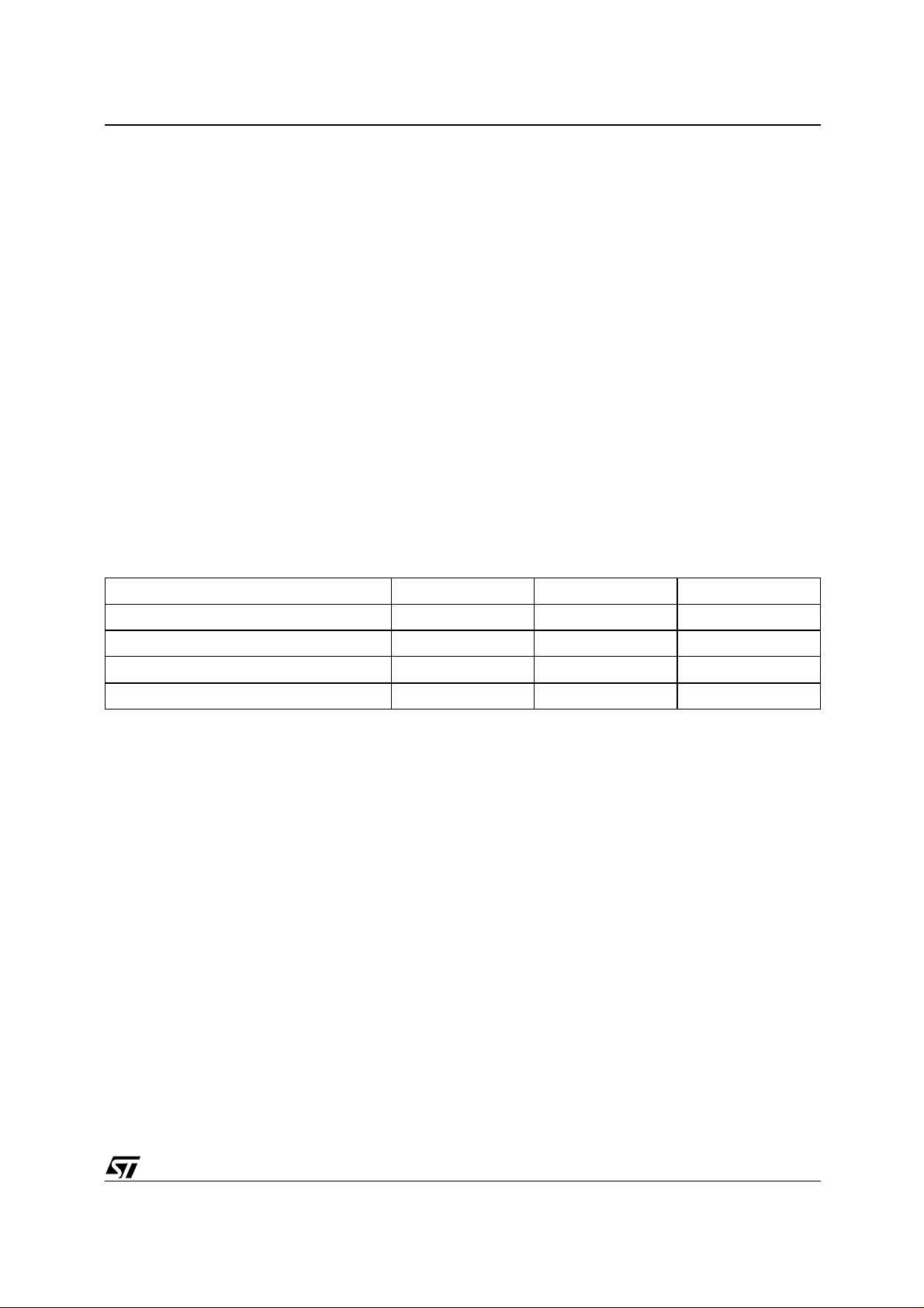
PSDsoft, a software development tool from ST,
guides you through the design process step-bystep making it possible to complete an embedded
MCU design capable of ISP/IAP in just hours. Select your MCU and PSDsoft takes you through the
remainder of the design with point and click entry,
covering PSD selection, pi n definitions, programmable logic inputs and outputs, MCU memory map
definition, ANSI-C code generation for you r MCU,
and merging your MCU firmware with the PSD design. When complete, two different device programmers are supported directly from PSDsoft:
FlashLINK (JTAG) and PSDpro.
This is preliminary information on a new product now in development or undergoing evaluation. Details are subject to change without notice.
9/100
PSD4256G6V
Figure 2. Logic Diagram Table 1. Pin Names
V
CC
8
PA0-PA7
PA0-PA7 Port-A
PB0-PB7 Port-B
PC0-PC7 Port-C
PD0-PD3 Port-D
CNTL0-
CNTL2
AD0-AD15
RESET
3
16
PSD4xxxGx
V
SS
8
8
4
8
8
8
PB0-PB7
PC0-PC7
PD0-PD3
PE0-PE7
PF0-PF7
PG0-PG7
AI04916
PE0-PE7 Port-E
PF0-PF7 Port-F
PG0-PG7 Port-G
AD0-AD15 Address/Data
CNTL0-CNTL2 Control
RESET
V
CC
V
SS
Reset
Supply Voltage
Ground
10/100
This is preliminary information on a new product now in development or undergoing evaluation. Details are subject to change without notice.
Figure 3. TQ FP 80 Connection s
PD1
PD0
PE7
80797877767574737271706968676665646362
PE6
PE5
PE4
PE3
PE2
PE1
PE0
GND
VCCPB7
PB6
PB5
PB4
PB3
PB2
PB1
PSD4256G6V
PB0
61
PD2
PD3
AD0
AD1
AD2
AD3
AD4
GND
V
CC
AD5
AD6
AD7
AD8
AD9
AD10
AD11
AD12
AD13
AD14
AD15
1
2
3
4
5
6
7
8
9
10
11
12
13
14
15
16
17
18
19
20
21222324252627282930313233343536373839
CC
PF0
PF1
PF2
PF3
PF4
PF5
PF6
PG0
PG1
PG2
PG3
PG4
PG5
PG6
PG7
V
GND
PF7
RESET
40
CNTL2
60 CNTL1
59 CNTL0
58 PA7
57 PA6
56 PA5
55 PA4
54 PA3
53 PA2
52 PA1
51 PA0
50 GND
49 GND
48 PC7
47 PC6
46 PC5
45 PC4
44 PC3
43 PC2
42 PC1
41 PC0
AI04943
This is preliminary information on a new product now in development or undergoing evaluation. Details are subject to change without notice.
11/100
PSD4256G6V
Table 2. TQFP80 Pin Description
Pin Name Pin Type Description
This is the lower Address/Data port. Connect your MCU address or address/data bus
according to the following rules:
1. If your MCU has a m ultiplexed ad dress/data bus where th e data is multi plexed with
the lower address bits, connect AD0-AD7 to this port.
ADIO0ADIO7
ADIO8ADIO15
CNTL0 59 I
3-7
10-12
13-20 I/O
I/O
2. If your MCU does not have a multiplexe d address/data bus, connect A0-A7 to this
port.
3. If you are usin g an 80C 51XA in b urst mode , connect A4/D0 thro ugh A11/D 7 to this
port.
ALE or AS latches the address. The PSD drives data out only if the READ signal is
active and one of the PSD functional blocks has been selected. The addresses on this
port are passed to the PLDs.
This is the upper Address/Data port. Connect your MCU address or address/data bus
according to the following rules:
1. If your MCU has a m ultiplexed ad dress/data bus where th e data is multi plexed with
the address bits, connect A8-A15 or AD8-AD15 to this port.
2. If your MCU do es not h ave a multiplexed address/da ta bus, conne ct A8-A15 to this
port .
3. If you are using an 80C51XA in burst mode, connect A12/D8 through A19/D15 to this
port.
ALE or AS latches the address. The PSD drives data out only if the READ signal is
active and one of the PSD functional blocks has been selected. The addresses on this
port are passed to the PLDs.
The following control signals can be connected to this pin, based on your MCU:
– active Low, WRITE Strobe input.
1. WR
– active High, READ/active Low WRITE input.
2. R_W
3. WRL
– active Low, WRITE to Low-byte.
This pin is connected to the PLDs. Therefore, these signals can be used in decode and
other logic equations.
CNTL1 60 I
CNTL2 40 I
RESET
PA0-PA7 51-58
39 I
I/O
CMOS
or
Open
Drain
The following control signals can be connected to this pin, based on your MCU:
1. 1RD
– active Low, READ Strobe input.
2. E – E clock input.
– active Low, Data Strobe input.
3. DS
– active Low, Strobe for low data byte.
4. LDS
This pin is connected to the PLDs. Therefore, these signals can be used in decode and
other logic equations.
READ or other Control input pin, with multiple configurations. Depending on the MCU
interface selected, this pin can be:
1. PSEN
2. BHE – High-byte enable, 16-bit data bus.
3. UDS
4. SIZ0 – Byte enable input.
5. LSTRB – Low Strobe input.
This pin is also connected to the PLDs.
Active Low input. Resets I/O Ports, PLD Macrocells and some of the Configuration
Registers and JT A G registers. Must be Low at Power-up. RESET also aborts any Flash
memory Program or Erase cycle that is currently in progress.
These pins make up Port A. These port pins are configurable and can have the
following functions:
1. MCU I/O – standard output or input port.
2. CPLD Macrocell (McellA0-McellA7) outputs.
3. Latched, transparent or registered PLD inputs (can also be PLD input for address A16
– Program Select Enable, a ctive Low in cod e retrieve bus cycle (80C51XA
mode).
– active Low, Strobe for high data byte, 16-bit data bus mode.
and above).
12/100
This is preliminary information on a new product now in development or undergoing evaluation. Details are subject to change without notice.
Pin Name Pin Type Description
These pins make up Port B. These port pins are configurable and can have the
following functions:
1. MCU I/O – standard output or input port.
2. CPLD Macrocell (McellB0-McellB7) outputs.
3. Latched, transparent or registered PLD inputs (can also be PLD input for address A16
and above).
These pins make up Port C. These port pins are configurable and can have the
following functions:
1. MCU I/O – standard output or input port.
2. External Chip Select (ECS0-ECS7) outputs.
3. Latched, transparent or registered PLD inputs (can also be PLD input for address A16
and above).
PB0-PB7 61-68
PC0-PC7 41-48
I/O
CMOS
or
Open
Drain
I/O
CMOS
PSD4256G6V
PD0 79
PD1 80
PD2 1
PD3 2
PE0 71
PE1 72
PE2 73
PE3 74
I/O
CMOS
or
Open
Drain
I/O
CMOS
or
Open
Drain
I/O
CMOS
or
Open
Drain
I/O
CMOS
or
Open
Drain
I/O
CMOS
or
Open
Drain
I/O
CMOS
or
Open
Drain
I/O
CMOS
or
Open
Drain
I/O
CMOS
or
Open
Drain
PD0 pin of Port D. This port pin can be configured to have the following functions:
1. ALE/AS input – latches address on ADIO0-ADIO15.
input – latches address on ADIO0-ADIO15 on the rising edge.
2. AS
3. MCU I/O – standard output or input port.
4. Transparent PLD input (can also be PLD input for address A16 and above).
PD1 pin of Port D. This port pin can be configured to have the following functions:
1. MCU I/O – standard output or input port.
2. Transparent PLD input (can also be PLD input for address A16 and above).
3. CLKIN – clock inpu t to the CPLD Macro cells, the APD Unit ’s Power-down cou nter,
and the CPLD AND Array.
PD2 pin of Port D. This port pin can be configured to have the following functions:
1. MCU I/O – standard output or input port.
2. Transparent PLD input (can also be PLD input for address A16 and above).
3. PSD Chip Select Input (CSI
I/O. When High, the PSD memory blocks are disabled to conserve power. The falling
edge of this signal can be used to get the device out of Power-down mode.
PD3 pin of Port D. This port pin can be configured to have the following functions:
1. MCU I/O – standard output or input port.
2. Transparent PLD input (can also be PLD input for address A16 and above).
3. WRH
PE0 pin of Port E. This port pin can be configured to have the following functions:
1. MCU I/O – standard output or input port.
2. Latched address output.
3. TMS Input for the JTAG Serial Interface.
PE1 pin of Port E. This port pin can be configured to have the following functions:
1. MCU I/O – standard output or input port.
2. Latched address output.
3. TCK Input for the JTAG Serial Interface.
PE2 pin of Port E. This port pin can be configured to have the following functions:
1. MCU I/O – standard output or input port.
2. Latched address output.
3. TDI input for the JTAG Serial Interface.
PE3 pin of Port E. This port pin can be configured to have the following functions:
1. MCU I/O – standard output or input port.
2. Latched address output.
3. TDO output for the JTAG Serial Interface.
– for 16-bit data bus, WRITE to high byte, active low.
). When Low, the MCU can access the PSD memory and
This is preliminary information on a new product now in development or undergoing evaluation. Details are subject to change without notice.
13/100
PSD4256G6V
Pin Name Pin Type Description
PE4 pin of Port E. This port pin can be configured to have the following functions:
1. MCU I/O – standard output or input port.
2. Latched address output.
3. TSTAT output for the JTAG Serial Interface.
4. Ready/Busy
output for parallel In-System Programming (ISP).
PE4 75
I/O
CMOS
or
Open
Drain
PE5 76
PE6 77
PE7 78
I/O
CMOS
or
Open
Drain
I/O
CMOS
or
Open
Drain
I/O
CMOS
or
Open
Drain
PE5 pin of Port E. This port pin can be configured to have the following functions:
1. MCU I/O – standard output or input port.
2. Latched address output.
3. TERR
active Low output for the JTAG Serial Interface.
PE6 pin of Port E. This port pin can be configured to have the following functions:
1. MCU I/O – standard output or input port.
2. Latched address output.
3. V
– SRAM standby voltage input for SRAM battery backup.
STBY
PE7 pin of Port E. This port pin can be configured to have the following functions:
1. MCU I/O – standard output or input port.
2. Latched address output.
3. Battery-on Indicator (V
nal battery.
). Goes High when power is being drawn from the exter-
BATON
These pins make up Port F. These port pins are configurable and can have the
following functions:
PF0-PF7 31-38
I/O
CMOS
or
Open
Drain
1. MCU I/O – standard output or input port.
2. External Chip Select (ECS0-ECS7) outputs, or inputs to CPLD.
3. Latched address outputs.
4. Address A1-A3 inputs in 80C51XA mode (PF0 is grounded)
5. Data bus port (D0-D7) in a non-multiplexed bus configuration.
6. Peripheral I/O mode.
7. MCU RESET Mode.
These pins make up Port G. These port pins are configurable and can have the
following functions:
1. MCU I/O – standard output or input port.
2. Latched address outputs.
3. Data bus port (D8-D15) in a non-multiplexed, 16-bit bus configuration.
4. MCU RESET Mode.
Supply Voltage
PG0-PG7 21-28
V
CC
9, 29,
69
I/O
CMOS
or
Open
Drain
8, 30,
GND
49,
Ground pins
50, 70
Note: Signal names that have multiple nam es or functions are defined using PSDsoft.
14/100
This is preliminary information on a new product now in development or undergoing evaluation. Details are subject to change without notice.
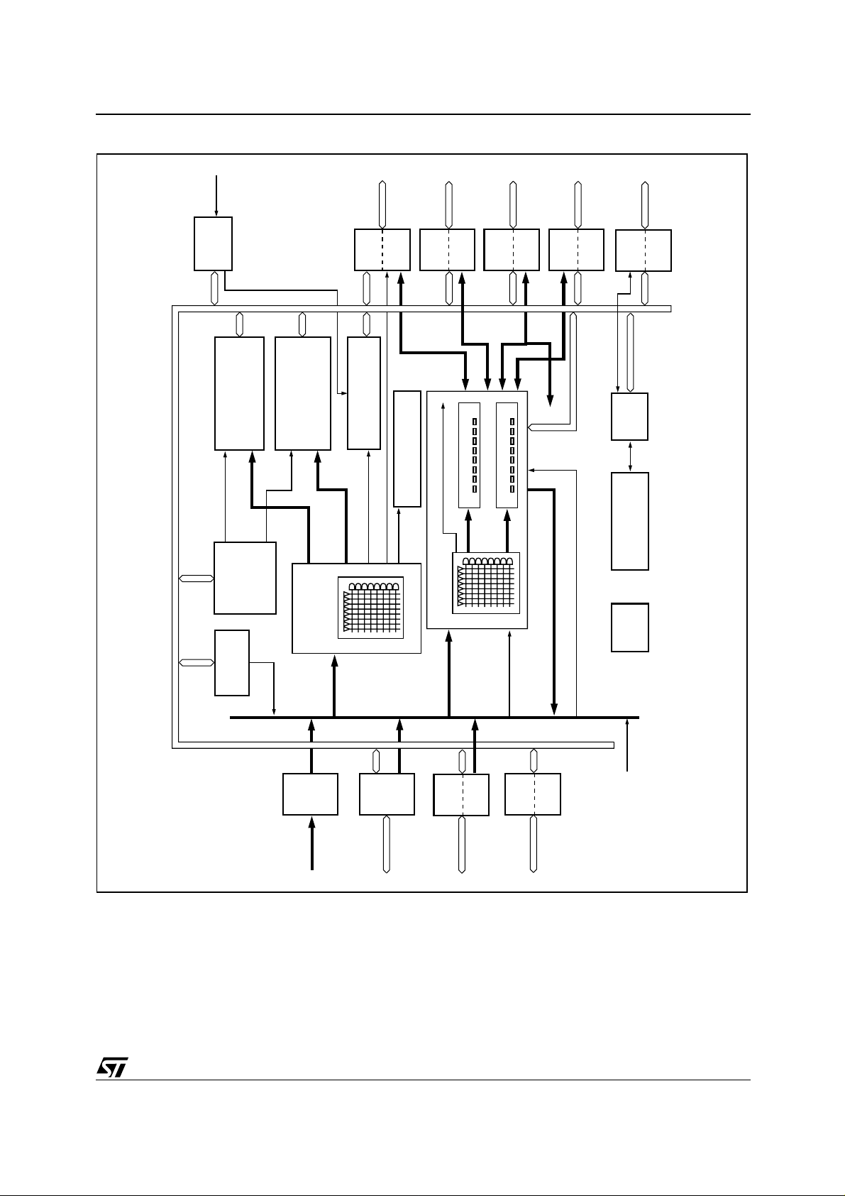
Figure 4. PSD Block Diagram
)
PE6
(
VSTDBY
PA0 – PA7
PB0 – PB7
PC0 – PC7
PD0 – PD3
PSD4256G6V
PE0 – PE7
POWER
ADDRESS/DATA/CONTROL BUS
UNIT
MANGMT
16 SECTORS
8 MBIT PRIMARY
FLASH MEMORY
EMBEDDED
ALGORITHM
PAGE
REGISTER
FLASH MEMORY
(BOOT OR DATA)
512 KBIT SECONDARY
SECTOR
SELECTS
FLASH DECODE
8
4 SECTORS
SECTOR
SELECTS
)
DPLD
(
PLD
82
A
PORT
PORT
PROG.
BACKUP SRAM
256 KBIT BATTERY
RUNTIME CONTROL
AND I/O REGISTERS
SRAM SELECT
PERIP I/O MODE SELECTS
CSIOP
B
PORT
PORT
PROG.
8 EXT CS TO PORT C or F
16 OUTPUT MACROCELLS
(CPLD)
FLASH ISP CPLD
82
PORT
PROG.
PORT A & B
PORT A ,B & C
24 INPUT MACROCELLS
CLKIN
C
PORT
PORT F
MACROCELL FEEDBACK OR PORT INPUT
PORT
PROG.
CLKIN
D
PORT
PROG.
JTAG
SERIAL
& FLASH MEMORY
PLD, CONFIGURATION
GLOBAL
CONFIG. &
PORT
PORT
CHANNEL
LOADER
SECURITY
E
PLD
BUS
INPUT
PROG.
CNTL0,
CNTL1,
INTRF.
MCU BUS
CNTL2
ADIO
PORT
AD0 – AD15
PORT
PROG.
PF0 – PF7
F
PORT
PORT
PROG.
PG0 – PG7
G
PORT
CLKIN
AI04917
Note: Additional address lines can be brought in to the device via Por t A , B, C, D, or F.
This is preliminary information on a new product now in development or undergoing evaluation. Details are subject to change without notice.
15/100
PSD4256G6V
PSD ARCHITECTURAL OVERVIEW
PSD devices contain several major functional
blocks. Figure 4, page 15 shows the architecture
of the PSD device family. The functions of each
block are described briefly in the following sections. Many of th e blocks perform multiple functions and are user configurable.
Memory
Each of the memory blocks is briefly discussed in
the following paragraphs. A more det ailed discussion can be found in the section entitled “Memory
Blocks“ on page 25.
The 8Mbit primary Flash memory is the main
memory of the PSD. It is divided into 16 equallysized sectors that are individually selectable.
The 512Kbit secondary Flash memory is di vided
into 4 sectors. Each sector is individually selectable.
The 256Kbit SRAM is intended for use as a
scratch-pad memory or as an extension to the
MCU SRAM. If an external battery is connected to
the PSD’s Voltage Standby (V
data is retained in the event of power failure.
Each memory block can be located in a different
address space as defined by the user. The access
times for all memory types includes the address
latching and DPLD decoding time.
PLDs
The device contains two PLD blocks, the Decode
PLD (DPLD) and the Complex PLD (CPLD), as
shown in Table 2, page 12, each optimized for a
different function. The functional partitioning of the
PLDs reduces power consumption, optimizes
cost/performance, and eases design entry.
The DPLD is used to decode addresses and to
generate Sector Select signals for the PSD internal memory and regis ters. The DPLD has combinatorial outputs, while the CPLD can implement
more general user-defined logic functions. The
CPLD has 16 Output Macrocells (OMC) and 8
combinatorial outputs. The PSD also has 24 Input
Macrocells (IMC) that can be configured as inputs
to the PLDs. The PLDs receive their inputs from
the PLD Input Bus an d are different iated by their
output destinations, number of product terms, and
Macrocells.
The PLDs consume minimal power. The speed
and power consumption of the PLD i s controlled
by the Turbo Bit in PMMR0 and other bits in
PMMR2. These registers are set by the MCU at
, PE6) signal,
STBY
run-time. There is a slight penalty to PLD propagation time when not in the Turbo mode.
I/O Po r t s
The PSD has 52 I/O pins divided among seven
ports (Port A, B, C, D, E , F, and G). Each I/O pin
can be individually configured for different functions. Ports can be configured as standard MCU I/
O ports, PLD I/O, or latched address outputs for
MCUs using multiplexed address/data buses.
The JTAG pins can be e nabled on Port E for InSystem Programming (ISP).
MCU Bus Interface
The PSD easily interfaces with most 8-bit or 16-bit
MCUs, either with multiplexed or non-multiplexed
address/data buses. The device is configured to
respond to the MCU’s control pins, which are also
used as inputs to the PLDs.
ISP via JTAG Port
In-System Programming (ISP) can be pe rformed
through the JTAG signals on Port E. This serial interface allows complete programming of the entire
PSD MODULE device. A blank device can be
completely programmed. The JTAG signals (TMS,
TCK, TSTAT, TERR
, TDI, TDO) can be multiplexed with other functions on Port E. Table 3 indicates the JTAG pin assignm ent s.
Table 3. PLD I/O
Name Inputs Outputs
Decode PLD (DPLD) 82 17 43
Complex PLD (CPLD) 82 24 150
Product
Terms
Table 4. JTAG Signals on Port E
Port E Pins JTAG Signal
PE0 TMS
PE1 TCK
PE2 TDI
PE3 TDO
PE4 TSTAT
PE5 TERR
16/100
This is preliminary information on a new product now in development or undergoing evaluation. Details are subject to change without notice.
In-Syst em Prog r a mmi ng ( ISP)
Using the JTAG signals on Port E, the entire PSD
device (memory, logic, configuration) can be programmed or erased without the use of the MCU.
In-Application Programming (IAP)
The primary Flash memory can also be programmed, or re-programmed, in-system by the
MCU executing the programming algorithms out of
the secondary Flash memory, or SRAM. The secondary Flash memory can be programmed the
same way by executing out of the primary Flash
memory. Table 5, page 17 indicates which programming methods can program different functional blocks of the PSD.
Page Regist er
The 8-bit Page Register expands the address
range of the MCU by up to 256 times. The paged
address can be used as part of the address space
to access external memory and peripherals, or internal memory and I/O. The Page Register can
also be used to change the address mapping of
PSD4256G6V
the Flash memory blocks into different memory
spaces for IAP.
Power Management Unit (PMU)
The Power Management Unit (PMU) gives the
user control of the power consumption on selected
functional blocks based on system req uirements.
The PMU includes an Automatic Power-down
(APD) Unit that turns off device functions during
MCU inactivity. The APD Unit has a Power-down
mode that helps reduce power consumption.
The PSDalso has some bits that are configured at
run-time by the MCU to reduce power consumption of the CPLD. The Turbo Bit in PMMR0 can be
reset to ’0’ and the CPLD latches its outputs and
goes to Standby Mode un til the next transition on
its inputs.
Additionally, bits in PMMR2 can be set by the
MCU to block signals from entering the CPLD to
reduce power consumption. See th e section entitled “POWER MANAGEMENT” on page 70 for
more details.
Table 5. Methods of Programming Different Functional Blocks of the PSD
Functional Block JTAG-ISP Device Programmer IAP
Primary Flash Memory Yes Yes Yes
Secondary Flash memory Yes Yes Yes
PLD Array (DPLD and CPLD) Yes Yes No
PSD Configuration Yes Yes No
This is preliminary information on a new product now in development or undergoing evaluation. Details are subject to change without notice.
17/100
PSD4256G6V
DEVELOPMENT SYST EM
The PSD family is supported by PSDsoft, a Windows-based software development tool (Windows-95, Windows-98, Windows-NT). A PSD
design is quickly and easily produced in a point
and click environment. The designer does not
need to enter Hardware Description Language
(HDL) equations, unless desired, to define PSD
pin functions and memo ry map information. The
general design flow is shown in Figure 5. PSDsoft
is available from our web site (the address is given
Figure 5. PSDsoft Development Tool
Choose MCU and PSD
Automatically configures MCU
bus interface and other
PSD attributes
Define PSD Pin and
Node Functions
Point and click definition of
PSD pin functions, internal nodes,
and MCU system memory map
on the back page of this data sheet) or other distribution channels.
PSDsoft directly supports two low cost device programmers form ST: PSDpro and FlashLINK
(JTAG). Both of these prog rammers may be purchased through your local distributor/representative, or directly from our web site using a credit
card. The PSD is also supported by third party device programmers. See our web site for the current
list.
Define General Purpose
Logic in CPLD
Point and click definition of combinatorial and registered logic in CPLD.
Access HDL is available if needed
Merge MCU Firmware
with PSD Configuration
A composite object file is created
containing MCU firmware and
PSD configuration
*.OBJ FILE
PSD Programmer
PSDPro, or
FlashLINK (JTAG)
MCU FIRMWARE
HEX OR S-RECORD
FORMAT
*.OBJ FILE
AVAILABLE
FOR 3rd PARTY
PROGRAMMERS
(CONVENTIONAL or
JTAG-ISC)
C Code Generation
GENERATE C CODE
SPECIFIC TO PSD
FUNCTIONS
USER'S CHOICE OF
MICROCONTROLLER
COMPILER/LINKER
AI04919
18/100
This is preliminary information on a new product now in development or undergoing evaluation. Details are subject to change without notice.
PSD4256G6V
PSD REGISTER DESCRIPTION AND ADDRESS OFFSETS
Table 6 shows the offset addresses to the PSD
registers relative to the CSIOP base address. The
CSIOP space is the 256 bytes of address that is allocated by the user to the internal PS D registers.
Table 6. Register Address Offset
Register Name
Data In 00 01 10 11 30 40 41 Reads Port pin as input, MCU I/O input mode
Control 32 42 43
Data Out 04 05 14 15 34 44 45
Direction 06 07 16 17 36 46 47 Configures Port pin as input or output
Drive Select 08 09 19 38 49
Input Macrocell 0A 0B 1A Reads Input Macrocells
Port APort BPort CPort DPort EPort FPort
Table 6 provides brief descriptions of the registers
in CSIOP space. The following sections give a
more detailed description.
(1)
Other
G
Selects mode between MCU I/O or Address
Out
Stores data for output to Port pins, MCU I/O
output mode
Configures Port pins as either CMOS or
Open Drain
Description
Enable Out 0C 0D 1C 4C
Output
Macrocells A
Output
Macrocells B
Mask
Macrocells A
Mask
Macrocells B
Flash Memory
Protection 1
Flash Memory
Protection 2
Flash Boot
Protection
JTAG Enable C7 Enables JTAG Port
PMMR0 B0 Power Management Register 0
PMMR2 B4 Power Management Register 2
Page E0 Page Register
VM E2
20
21
22 Blocks writing to the Output Macrocells A
23 Blocks writing to the Output Macrocells B
Reads the status of the output enable to the I/
O Port driver
READ – reads output of Macrocells A
WRITE – loads Macrocell Flip-flops
READ – reads output of Macrocells B
WRITE – loads Macrocell Flip-flops
C0 Read only – Primary Flash Sector Protection
C1 Read only – Primary Flash Sector Protection
Read only – PSD Security and Secondary
C2
Flash memory Sector Protection
Places PSD memory areas in Program and/
or Data space on an individual basis.
Memory_ID0 F0 Read only – SRAM and Primary memory size
Memory_ID1 F1
Note: 1. Other registers that are not part of the I/O ports.
This is preliminary information on a new product now in development or undergoing evaluation. Details are subject to change without notice.
Read only – Secondary memory type and
size
19/100
PSD4256G6V
REGISTER BIT DEFINITION
All the registers of the PSD are included here, for
reference. Detailed descriptions of these registers
can be found in the following sections.
Table 7. Data-In Registers - Ports A, B, C, D, E, F, and G
Bit 7 Bit 6 Bit 5 Bit 4 Bit 3 Bit 2 Bit 1 Bit 0
Port pin 7 Port pin 6 Port pin 5 Port pin 4 Port pin 3 Port pin 2 Port pin 1 Port pin 0
Note: Bit Definit i ons (Read only register s):
READ Port pi n status when Port is in MCU I/O input mod e.
Table 8. Data-Out Registers - Ports A, B, C, D, E, F, and G
Bit 7 Bit 6 Bit 5 Bit 4 Bit 3 Bit 2 Bit 1 Bit 0
Port pin 7 Port pin 6 Port pin 5 Port pin 4 Port pin 3 Port pin 2 Port pin 1 Port pin 0
Note: Bit Definitio ns :
Latched data for output to Port pin when pin is conf i gured in MCU I/ O output mode.
Table 9. Direction Registers - Ports A, B, C, D, E, F, and G
Bit 7 Bit 6 Bit 5 Bit 4 Bit 3 Bit 2 Bit 1 Bit 0
Port pin 7 Port pin 6 Port pin 5 Port pin 4 Port pin 3 Port pin 2 Port pin 1 Port pin 0
Note: Bit Definitio ns :
Portpin <i> 0 = Port pin <i> is conf i gured in Input m ode (default ).
Portpin <i> 1 = Port pin <i> is configured in Output mode.
Table 10. Control Registers - Ports E, F, and G
Bit 7 Bit 6 Bit 5 Bit 4 Bit 3 Bit 2 Bit 1 Bit 0
Port pin 7 Port pin 6 Port pin 5 Port pin 4 Port pin 3 Port pin 2 Port pin 1 Port pin 0
Note: Bit Definitio ns :
Portpin <i> 0 = Port pin <i> is conf i gured in MCU I/O mode (defaul t).
Portpin <i> 1 = Port pin <i> is conf i gured in Latc hed Address Out mode.
Table 11. Drive Registers - Ports A, B, D, E, and G
Bit 7 Bit 6 Bit 5 Bit 4 Bit 3 Bit 2 Bit 1 Bit 0
Port pin 7 Port pin 6 Port pin 5 Port pin 4 Port pin 3 Port pin 2 Port pin 1 Port pin 0
Note: Bit Definitio ns :
Portpin <i> 0 = Port pin <i> is configured for CMOS Output driver (def ault).
Portpin <i> 1 = Port pin <i> is configured for Open Drain output driv er.
Table 12. Enable-Out Registers - Ports A, B, C, and F
Bit 7 Bit 6 Bit 5 Bit 4 Bit 3 Bit 2 Bit 1 Bit 0
Port pin 7 Port pin 6 Port pin 5 Port pin 4 Port pin 3 Port pin 2 Port pin 1 Port pin 0
Note: Bit Definit i ons (Read only register s):
Portpin <i> 0 = Port pin <i> is in tri-state driver (default).
Portpin <i> 1 = Port pin <i> is enabled.
20/100
This is preliminary information on a new product now in development or undergoing evaluation. Details are subject to change without notice.

PSD4256G6V
Table 13. Input Macrocells - Ports A, B, and C
Bit 7 Bit 6 Bit 5 Bit 4 Bit 3 Bit 2 Bit 1 Bit 0
IMcell 7 IMcell 6 IMcell 5 IMcell 4 IMcell 3 IMcell 2 IMcell 1 IMcell 0
Note: Bit Definit i ons (Read only register s):
READ Input Macrocell (IMC7-IMC0) status on Ports A, B, and C.
Table 14. Output Macrocells A Register
Bit 7 Bit 6 Bit 5 Bit 4 Bit 3 Bit 2 Bit 1 Bit 0
Mcella 7 Mcella 6 Mcella 5 Mcella 4 Mcella 3 Mcella 2 Mcella 1 Mcella 0
Note: Bit Definitio ns :
WRITE Register: Load MCellA7-MCellA0 with ’0’ or ’1.’
READ Re gi ster: Read M CellA7-MC el l A0 output st at us.
Table 15. Out Macrocells B Register
Bit 7 Bit 6 Bit 5 Bit 4 Bit 3 Bit 2 Bit 1 Bit 0
Mcellb 7 Mcellb 6 Mcellb 5 Mcellb 4 Mcellb 3 Mcellb 2 Mcellb 1 Mcellb 0
Note: Bit Definitio ns :
WRITE Register: Load MCellB7-MCellB0 with ’0’ or ’1.’
READ Re gi ster: Read M CellB7-MC el l B0 output st at us.
Table 16. Mask Macrocells A Register
Bit 7 Bit 6 Bit 5 Bit 4 Bit 3 Bit 2 Bit 1 Bit 0
Mcella 7 Mcella 6 Mcella 5 Mcella 4 Mcella 3 Mcella 2 Mcella 1 Mcella 0
Note: Bit Definitio ns :
McellA<i>_P rot 0 = Allow MCellA <i > flip-flop to be lo aded by MCU (default).
McellA<i>_Prot 1 = Prevent MCellA<i> flip-flop from bein g lo aded by MCU.
Table 17. Mask Macrocells B Register
Bit 7 Bit 6 Bit 5 Bit 4 Bit 3 Bit 2 Bit 1 Bit 0
Mcellb 7 Mcellb 6 Mcellb 5 Mcellb 4 Mcellb 3 Mcellb 2 Mcellb 1 Mcellb 0
Note: Bit Definitio ns :
McellB<i>_Pro t 0 = Allow MCellB<i> flip-flop to be loaded by MCU (default).
McellB<i>_Pro t 1 = Prevent M Cel l B <i > flip-flo p from being loaded by MCU.
Table 18. Flash Memory Protection Register 1
Bit 7 Bit 6 Bit 5 Bit 4 Bit 3 Bit 2 Bit 1 Bit 0
Sec7_Prot Sec6_Prot Sec5_Prot Sec4_Prot Sec3_Prot Sec2_Prot Sec1_Prot Sec0_Prot
Note: Bit Definitions (Read only register):
Sec<i>_Prot 1 = Primary Flash mem ory Sector <i> i s wr i te protected.
Sec<i>_Prot 0 = Primary Flash mem ory Sector <i> i s not write prote ct ed.
Table 19. Flash Memory Protections Register 2
Bit 7 Bit 6 Bit 5 Bit 4 Bit 3 Bit 2 Bit 1 Bit 0
Sec15_Prot Sec14_Prot Sec13_Prot Sec12_Prot Sec11_Prot Sec10_Prot Sec9_Prot Sec8_Prot
Note: Bit Definitions (Read only register):
Sec<i>_Prot 1 = Primary Flash mem ory Sector <i> i s wr i te protected.
Sec<i>_Prot 0 = Primary Flash mem ory Sector <i> i s not write prote ct ed.
This is preliminary information on a new product now in development or undergoing evaluation. Details are subject to change without notice.
21/100

PSD4256G6V
Table 20. Flash Boot Protection Register
Bit 7 Bit 6 Bit 5 Bit 4 Bit 3 Bit 2 Bit 1 Bit 0
Security_Bit not used not used not used Sec3_Prot Sec2_Prot Sec1_Prot Sec0_Prot
Note: Bit Definitio ns :
Sec<i>_Prot 1 = Secondary Flash m em ory Sector <i > is write protected.
Sec<i>_Prot 0 = Secondary Flash m em ory Sector <i > is not write pro tected.
Security_Bit 0 = Securit y B it in device has not been set.
Security_Bit 1 = Securit y B it in device has been set.
Table 21. JTAG Enable Register
Bit 7 Bit 6 Bit 5 Bit 4 Bit 3 Bit 2 Bit 1 Bit 0
not used not used not used not used not used not used not used JTAGEnable
Note: Bit Definitio ns :
JTAGEnable 1 = J T AG Port is enabled.
JTAGEnable 0 = J T AG Port is disabl ed.
Table 22. Page Register
Bit 7 Bit 6 Bit 5 Bit 4 Bit 3 Bit 2 Bit 1 Bit 0
PGR 7 PGR 6 PGR 5 PGR 4 PGR 3 PGR 2 PGR 1 PGR 0
Note: Bit Definitio ns :
Configure Page input to PLD. Default is PGR7-PGR0 = ’0.’
22/100
This is preliminary information on a new product now in development or undergoing evaluation. Details are subject to change without notice.
PSD4256G6V
Table 23. PMMR0 Register
Bit 7 Bit 6 Bit 5 Bit 4 Bit 3 Bit 2 Bit 1 Bit 0
not used
(set to 0)
Note: The bits of this re gister are cleared to zero following power-up. Subsequent Reset (RESET) pulses do not clea r the registers.
Bit Definitions :
APD Enable 0 = Automatic Power-down (APD) is disabled.
PLD Turbo 0 = PLD Turbo is on.
PLD Array CLK 0 = CLKIN to the PLD AND array is connec t ed. Every CLK I N change powers up the PLD when Turbo B i t is off.
PLD MCells CLK 0 = CLKIN to the PLD Macrocel l s is connec ted.
Table 24. PMMR2 Register
Bit 7 Bit 6 Bit 5 Bit 4 Bit 3 Bit 2 Bit 1 Bit 0
not used
(set to 0)
Note: F or Bit 4, Bit 3, Bit 2: See Table 34, page 47 for the signals that are blocked on pins CNT L0-CNTL2.
Bit Definitions :
PLD Array Addr 0 = Address A7-A0 are connect ed to the PLD arr ay.
PLD Array CNTL2 0 = CN T L2 input to th e PLD AND array is connected.
PLD Array CNTL1 0 = CN T L1 input to th e PLD AND array is connected.
PLD Array CNTL0 0 = CN T L0 input to th e PLD AND array is connected.
PLD Array ALE 0 = ALE input to th e PLD AND array is connec ted.
PLD Array WRH 0 = WRH/DBE input to the PLD AN D array is connected.
not used
(set to 0)
1 = Automatic Power-down (APD) is enabled.
1 = PLD Turbo is off, saving power.
1 = CLKIN to the PLD AND arra y i s disconnec t ed, saving power.
1 = CLKIN to the PLD Macrocel l s is disconnected, sav i ng power.
PLD
Array WRH
1 = Address A7-A0 are blocked from the P LD array, sa ving power.
Note: In X A Mode, A3-A0 c om e from PF3-P F 0, and A7-A4 come from ADIO 7-ADIO4.
1 = CNTL2 input to the PLD AND array is disconnected, saving po wer.
1 = CNTL1 input to the PLD AND array is disconnected, saving po wer.
1 = CNTL0 input to the PLD AND array is disconnected, saving po wer.
1 = ALE input to the PLD AND array is disco nnected, saving power.
1 = WRH/DBE i nput to the PLD AN D array is disconnected, saving power.
PLD
MCells CLK
PLD
Array ALE
PLD
Array CLK
PLD Array
CNTL2
PLD
Turbo
PLD Array
CNTL1
not used
(set to 0)
PLD Array
CNTL0
APD
Enable
not used
(set to 0)
not used
(set to 0)
PLD
Array Addr
Table 25. VM Register
Bit 7 Bit 6 Bit 5 Bit 4 Bit 3 Bit 2 Bit 1 Bit 0
Peripheral
mode
Note: On RESET, Bits 1-4 are loaded to configurations that are selected by the user in PSDsoft. Bit 0 and Bit 7 are always cleared on RESET.
Bit 0-4 are active only when the device is configu red in 8051 Mode.
Bit Definitions :
SR_code 0 = PSEN
Boot_Code 0 = PSEN
FL_Code 0 = PSEN
Boot_data 0 = RD
FL_data 0 = RD
Peripheral mode 0 = Peripher al m ode of Port F is disabled.
This is preliminary information on a new product now in development or undergoing evaluation. Details are subject to change without notice.
not used
(set to 0)
1 = PSEN
1 = PSEN
1 = PSEN
1 = RD
1 = RD
1 = Peripher al mode of Port F is enabled.
not used
(set to 0)
cannot access SRAM in 80C51XA modes.
can access SRAM in 80 C5 1 XA mod es.
cannot access Secondary NVM in 80C51XA mo des.
can access Sec on d ar y NVM i n 80C5 1 X A mode s.
cannot acc ess Primary Flash memory i n 80C51XA mod es.
can access Primary Flash memory in 8 0C51XA modes.
cannot acc ess Secondary NVM in 80C51XA modes .
can access Secondary NVM in 80C51XA modes.
cannot acc ess Primary Flash memory i n 80C51XA mod es.
can access Primary Flash memory in 80C51XA modes.
FL_data Boot_data FL_code Boot_code SR_code
23/100

PSD4256G6V
Table 26. Memory_ID0 Register
Bit 7 Bit 6 Bit 5 Bit 4 Bit 3 Bit 2 Bit 1 Bit 0
S_size 3 S_size 2 S_size 1 S_size 0 F_size 3 F_size 2 F_size 1 F_size 0
Note: Bit Definitio ns :
F_size[3:0] 0h = There is no Prima ry Flash memory
1h = Primary Flash memory size is 256Kbit
2h = Primary Flash memory size is 512Kbit
3h = Primary Flash memory size is 1Mbit
4h = Primary Flash memory size is 2Mbit
5h = Primary Flash memory size is 4Mbit
6h = Primary Flash memory size is 8Mbit
S_size[3:0] 0h = There is no SRAM
Table 27. Memory_ID1 Register
Bit 7 Bit 6 Bit 5 Bit 4 Bit 3 Bit 2 Bit 1 Bit 0
not used
(set to 0)
Note: Bit Definitio ns :
F_size[3:0] 0h = There is no Secon dary NVM
S_size[3:0] 0h = Secondary NVM is Flash memory
1h = SRAM size is 16Kbit
2h = SRAM size is 32Kbit
3h = SRAM size is 64Kbit
4h = SRAM size is 128Kbit
5h = SRAM size is 256Kbit
not used
(set to 0)
1h = Secondar y NVM size is 128 Kbit
2h = Secondar y NVM size is 256 Kbit
3h = Secondar y NVM size is 512 Kbit
1h = Secondary NVM is EEPROM
B_type 1 B_type 0 B_size 3 B_size 2 B_size 1 B_size 0
24/100
This is preliminary information on a new product now in development or undergoing evaluation. Details are subject to change without notice.

DETAILED OPERATION
As shown in Figure 4, page 15, the PSD consists
of six major types of functional blocks:
■ Memory Blocks
■ MCU Bus Interface
■ I/O Ports
■ Power Management Unit (PMU)
■ JTAG-ISP Interface
■ The functions of each block are described in the
following sections. Many of the blocks perform
multiple functions, and are user configurable.
Table 28. Memory Block Size and Organization
Primary Flash Memory Secondary Flash Memory SRAM
Sector
Number
0 64K FS0 16K CSBOOT0 32K RS0
1 64K FS1 8K CSBOOT1
2 64K FS2 8K CSBOOT2
3 64K FS3 32K CSBOOT3
4 64K FS4
Sector Size
(Bytes)
Sector Select
Signal
Sector Size
PSD4256G6V
Memory Blocks
The PSD has the following memory blocks:
– Primary Flash memory
– Secondary Flash memory
–SRAM
The Memory Select signals for these blocks origi-
nate from the Decode PLD (DPLD) an d are userdefined in PSDsoft.
Table 28 summarizes the sizes and organizations
of the memory blocks.
(Bytes)
Sector Select
Signal
SRAM Size
(Bytes)
SRAM Select
Signal
5 64K FS5
6 64K FS6
7 64K FS7
8 64K FS8
9 64K FS9
10 64K FS10
11 64K FS11
12 64K FS12
13 64K FS13
14 64K FS14
15 64K FS15
Total 1024K 16 Sectors 64K 4 Sectors 32K
This is preliminary information on a new product now in development or undergoing evaluation. Details are subject to change without notice.
25/100

PSD4256G6V
Primary Flash Mem ory an d Sec on dary F lash me m ory Desc rip tion
The primary Flash memory is divided evenly into 8
sectors. The secondary Flash m emory is divided
into 4 sectors of different size. Each sector of either memory block can be separately protected
from Program and Erase cycles.
Flash memory may be erased on a sector-by-sector basis, and programmed word-by-word. Flash
sector erasure may be suspended while data is
read from other sectors o f the block and th en resumed after reading.
During a Program or Erase cycle in Flash memory,
the status can be output on the Ready/Busy
pin
(PE4). This pin is set up using PSDsoft.
Memory Block Select Signals
The DPLD generates the Select signals for all the
internal memory blocks (see the section entitled
“PLDs”, on page 38). Each of the sectors of the primary Flash memory has a Select signal (FS0FS15) which can contain up to three product
terms. Each of the sectors of the secondary Flash
memory has a Select signal (CSBOOT0CSBOOT3) which can contain up to three product
terms. Having three product terms for each Select
signal allows a given sector to be mapped in different areas of syste m memory. When using a MCU
with separate Program and Data space
(80C51XA), these flexible Select signals allow dynamic re-mapping of sectors from one memory
space to the other before and after IAP. The
SRAM block has a single Select signal (RS0).
Ready/Busy
(PE4)
This signal can be used to output the Ready/Busy
status of the PSD. The output is a '0' (Busy) when
a Flash memory block is being written to,
a Flash memory block is being erased. The output
is a '1' (Ready) when no WRITE or Erase cycle is
in progress.
Memory Operation
The primary Flash memory and secondary Flash
memory are addressed through the MCU Bus Interface. The MCU can access these memories in
one of two ways:
■ The MCU can execute a typical bus WRITE or
READ
operation
RAM or ROM device using standard bus cycles.
■ The MCU can execute a specific instruction that
consists of several WRITE and READ
operations. This involves writing specific data
patterns to special addresses within the Flash
memory to invoke an embedded algorithm.
These instructions are summarized in Table 29,
page 27.
Typically, the MCU can read Flash memory using
READ operations, just as it would read a ROM device. However, Flash memory can only b e erased
and programmed using specific instructions. For
example, the MCU c annot write a single byte directly to Flash memory as one would write a byte
to RAM. To program a word int o Flash memory,
the MCU must execute a Program instruction, then
test the status of the Programming event. This status test is achieved by a READ operation or polling
Ready/Busy
(PE4).
Flash memory can also be read by using special
instructions to retrieve particular Flash device information (sector protect status and ID).
or
when
just as it would if accessing a
26/100
This is preliminary information on a new product now in development or undergoing evaluation. Details are subject to change without notice.

PSD4256G6V
Table 29. 16-bit Instructions
Instruction
READ
(5)
(14)
READ Main Flash
(6, 13)
ID
READ Sector
Protection
(6,8,13)
Program a Flash
(13)
Word
Flash Sector
(7,13)
Erase
Flash Bulk Erase
(13)
Suspend Sector
(11)
Erase
Resume Sector
(12)
Erase
(6)
RESET
Unlock Bypass 1
Unlock Bypass
Program
(9)
Unlock Bypass
(10)
Reset
Note: 1. All bus cycles are WRITE bus cycles, ex cept the ones with the “Re ad” label
2. All v al ues are in hexadecimal:
X = “Don’t care.” Address es of the form XXXXh, in thi s t abl e, must be ev en addresse s
RA = Address of the memory l ocation to be read
RD = Data re ad f rom location RA during t h e READ cycle
PA = Address of the memory location to be programmed. Addresses are latched on the falling edge of WRITE Strobe (WR
PA is an even ad dress for PS D i n word program m i ng mode.
PD = Data word to be programm ed at location PA. Data is la tc hed on the rising edge of WR ITE Strobe (WR
SA = Address of the sector to be erased or verified. The Sector Select (FS0-FS15 or CSBOOT0-CSBOOT3) of the sector to be
erased, or verified, must be Active (High).
3. Sector Select (FS0 to FS15 or CSBOOT0 to CSBOOT3) signals are active High, and are defined in PSDsoft.
4. Only address bits A11-A0 are used in instruction decoding.
5. No U nl ock or instruction cycl es are required when the dev i ce is in the READ Mode
6. The R ES ET ins truc tio n is re quir ed t o ret urn t o the RE AD Mod e aft er rea ding the F la sh I D, or afte r read ing the S ect or Pr otec tion
Status, or if the Error Flag Bit (DQ5/DQ13) goes High.
7. Addi t i onal sectors to be erased must be written at the end of t he Sector Eras e i nstruction within 80µs.
8. The da ta is 00h for an unprotect ed sector, an d 01h for a prot ected secto r. In the fourt h cycle, the S ector Sele ct is active, an d
(A1,A0) = (1,0).
9. The Unlock Bypass instruction is required prior to the Unlock Bypass Program instruction.
10. The U nl ock Bypass Reset Fl ash instru ct i on is requ i red to return to reading memory data whe n t he device i s in the Unlock Bypass
mode.
11. The system may perform READ and Program cycles in non-erasing sectors, read the Flash ID or read the Sector Protection Status
when in the Suspend Sector Erase mo de. T he Suspend Sector Erase instruction is valid onl y during a Sector Erase cyc l e.
12. The Resume Sector Erase instruction is valid only during the Suspend Sector Erase mode.
13. The MCU can not inv oke the se in stru ction s whi le execu tin g code fr om the sa me Fla sh me mory as that fo r which th e ins truc tion is
intended. T he MCU mus t re tri eve, for exam pl e, the co de fr om the s econ dar y F lash m em ory wh en rea ding t he S ecto r Pr otec tion
Status of th e pri m ary Flash memory.
14. All WRITE bus cycles in an instruction are byte-WRITE to an even address (XA4Ah or X554h). A Flash memory Program bus cycle
writes a wo rd t o an even address.
FS0-FS15 or
CSBOOT0-
CSBOOT3
1
0
1
1
1
1
1
1
1
1
1
Cycle 1 Cycle 2 Cycle 3 Cycle 4 Cycle 5 Cycle 6 Cycle 7
“Read”
RD @ RA
AAh@
XAAAh
AAh@
XAAAh
AAh@
XAAAh
AAh@
XAAAh
AAh@
XAAAh
55h@
X554h
55h@
X554h
55h@
X554h
55h@
X554h
55h@
X554h
90h@
XAAAh
90h@
XAAAh
A0h@
XAAAh
80h@
XAAAh
80h@
XAAAh
Read ID
@ XX02h
Read 00h
or 01h @
XX04h
PD@ PA
AAh@
XAAAh
AAh@
XAAAh
55h@
X554h
55h@
X554h
30h@
SA
10h@
XAAAh
B0h@
XXXXh
30h@
XXXXh
F0h@
XXXXh
AAh@
XAAAh
A0h@
XXXXh
90h@
XXXXh
55h@
X554h
PD@ PA
00h@
XXXXh
20h@
XAAAh
, CNTL0)
(7)
30h
next SA
, CNTL0).
@
This is preliminary information on a new product now in development or undergoing evaluation. Details are subject to change without notice.
27/100

PSD4256G6V
INSTRUCTIONS
An instruction consists of a sequence o f specific
operations. Each received byte is sequentially decoded by the PSD and not executed as a standard
WRITE operation. The instruction is executed
when the correct number of bytes are properly received and the time between two consecutive
bytes is shorter than the time-out period. Some instructions are structured to include READ operations after the initial WRITE operations.
The instruction must be followed exactly. Any invalid combination of instruction bytes or time-out
between two consecutive byte s while addressing
Flash memory resets the device logic into READ
Mode (Flash memory is read like a ROM device).
The PSD supports the instructions summa rized in
Table 29, page 27:
■ Erase memory by chip or sector
■ Suspend or resume sector erase
■ Program a Word
■ RESET to READ Mode
■ READ Primary Flash Identifier value
■ READ Sector Protection Status
■ Bypass
These instructions are detailed in Table 29, page
27. For efficient decoding of the ins tructions, the
first two bytes of an instruction are the coded cycles and are followed by an instruction byte or confirmation byte. The coded cycles consist of writing
the data AAh to address XAAAh during the first cycle and data 55h to address X554h during the second cycle (unless the Bypass instruction feature is
used, as described later). Address signals A15A12 are “Don’t care” during the instruction WRITE
cycles. However, the appropriate Sector Select
signal (FS0-FS15, or CSBOOT0-CSBOOT3) must
be selected.
The primary and secondary Flash memories have
the same instruction set (except for READ Primary
Flash Identifier). The Sector Select signals determine which Flash memory is to receive and execute the instruction. The primary Flash memory is
selected if any one of its Sector Select signals
(FS0-FS15) is High, and the secondary Flash
memory is selected if any one of its Sector Select
signals (CSBOOT0-CSBOOT3) is High.
Power-up Condition
The PSD internal logic is reset upon Power-up to
the READ Mode. Sector Select (FS0-FS15 and
CSBOOT0-CSBOOT3) must be held Low, and
WRITE Strobe (WR
/WRL, CNTL0) High, during
Power-up for maximum security of the data contents and to remove the possibility of data being
written on the first edge of WRITE Strobe (WR
WRL
, CNTL0). Any WRITE cycle initiation is
locked when V
is below V
CC
LKO
.
READ
Under typical conditions, the MCU may read the
primary Flash memory, or secondary Flash memory, using READ operations just as it would a
ROM or RAM device. Alternately, the MCU may
use READ operations to obtain s tatus inform ation
about a Program or Erase cycle that is currently in
progress. Lastly, the MCU may use instructions to
read special data from these memory blocks. The
following sections describe these READ functions.
READ Memory Con tents
Primary Flash memory and secondary Flash
memory are placed in the READ Mode after Power-up, chip reset, or a Reset Flash instruction (see
Table 29, page 27). The MCU can read th e memory contents of the primary Flash memory, or the
secondary Flash memory by using READ operations any time the READ operation is not part of an
instruction .
READ Primary Flash Identifier
The primary Flash mem ory identifier is read with
an instruction composed of 4 operations: 3 specific
WRITE operations and a READ operation (see Table 29, page 27). The identifier for the primary
Flash memory is E7h. The secondary Flash memory does not support this instruction.
READ Memory Sector Protection Status
The Flash memory Sector Protection Status is
read with an instruction composed of four operations: three specific WRITE operations and a
READ operation (see Table 29, page 27). The
READ operation produces 01h if the Flash memory sector is protected, or 00h if the sector is not
protected.
The sector protection status for all NVM blocks
(primary Flash memory, or secondary Flash memory) can be read by the MCU accessing the Flash
Protection and F lash Boot Protection registers in
PSD I/O space. See the section entitled “Flash
Memory Sector Protect”, on page 34, for register
definitions.
/
28/100
This is preliminary information on a new product now in development or undergoing evaluation. Details are subject to change without notice.
PSD4256G6V
Reading the Erase/Program Status Bits
The PSD provides several st atus bits to be used
by the MCU to confirm the completion of an Erase
or Program cycle of Flash memory. These status
bits minimize the time that the MCU spends performing these tasks and are defined in Table 30.
The status byte resides in an even location, and
can be read as many times as needed. Also note
Table 30. Status Bits
DQ7 DQ6 DQ5 DQ4 DQ3 DQ2 DQ1 DQ0
Data Polling Toggle Flag Error Flag X
Table 31. Status Bits for Motorola 16-bit MCU
DQ15 DQ14 DQ13 DQ12 DQ11 DQ10 DQ9 DQ8
Data Polling Toggle Flag Error Flag X
Notes:X = Not guaranteed value, can be read either ’1’ or ’0.’
DQ15-DQ0 represent the Data Bus bits, D15-D0.
FS0-FS15/CSBOOT 0-CSBOO T 3 are active High.
that DQ15-DQ8 is an even byte for Motorola
MCUs with a 16-bit data bus.
For Flash memory, the MCU can perform a READ
operation to obtain these status bits while an
Erase or Program instruction is being executed by
the embedded algorithm. See the section entit led
“PROGRAMMING FLASH MEMORY”, on page
31, for details.
Erase Time-
out
Erase Time-
out
XXX
XXX
This is preliminary information on a new product now in development or undergoing evaluation. Details are subject to change without notice.
29/100

PSD4256G6V
Data Polling (DQ7) - DQ15 for Motorola
When erasing or programm ing in Flash memory,
the Data Polling Bit (DQ7/DQ15) outputs the complement of the bit being entered for programming/
writing on the DQ7/DQ15 Bit. Once the Program
instruction or the WRITE operation is completed,
the true logic value is read on t he Data P ol ling Bit
(DQ7/DQ15) (in a READ operation).
■ Data Polling is effective after the fourth WRITE
pulse (for a Program instruction) or after the
sixth WRITE pulse (for an Erase instruction). It
must be performed at the address being
programmed or at an address within the Flash
memory sector being erased.
■ During an Erase cycle, the Data Polling Bit
(DQ7/DQ15) outputs a ’0.’ After completion of
the cycle, the Data Polli n g Bit (DQ7/ DQ15)
outputs the last bit programmed (it is a ’1’ after
erasing).
■ If the location to be programmed is in a
protected Flash memory sector, the instruction
is ignored.
■ If all the Flash memory sectors to be erased are
protected, the Data Polling Bit (DQ7/DQ15) is
reset to '0' for about 100µs, and then returns to
the value from the previously addressed
location. No erasure is performed.
Toggle Flag (DQ6) – DQ14 for Motorola
The PSD offers another way for determining when
the Flash memory Program cycle is completed.
During the internal WRITE operation and when either FS0-FS15 or CSBOOT0-CSBOOT3 is true,
the Toggle Flag Bit (DQ6/DQ14) toggles from 0 to
’1’ and ’1’ to ’0’ on subsequent attempts to read any
word of the memory .
When the internal cycle is complete, the toggling
stops and the data read on the Data Bus D0-D7 is
the value from the addressed memory location.
The device is now ac cessible for a new READ or
WRITE operation. The cycle is finished when t wo
successive READs yield the same output data.
■ The Toggle Flag Bit (DQ6/DQ14) is effective
after the fourth WRITE pulse (for a Program
instruction) or after the sixth WRITE pulse (for
an Erase instruction).
■ If the location to be programmed belongs to a
protected Flash memory sector, the instruction
is ignored.
■ If all the Flash memory sectors selected for
erasure are protected, the Toggle Flag Bit
(DQ6/DQ14) toggles to '0' for about 100µs and
then returns to the value from the previously
addressed location.
Error Flag (DQ5) – DQ13 for Motorola
During a normal Program or Erase cycle, the Error
Flag Bit (DQ5/DQ13) is reset to ’0.’ This bit is set
to ’1’ when there is a failure during a Flash memory
Program, Sector Erase, or Bulk Erase cycle.
In the case of Flash memory programming, the Error Flag Bit (DQ5/DQ13) indicates the attempt to
program a Flash memory bit, or bits, from the programmed state, 0, to the erased state, ’1,’ which is
not a valid operation. The Error Flag Bit (DQ5/
DQ13) may also indicate a Time-out condition
while attempting to program a word.
In case of an error in a Flash memory Sector Erase
or Word Program cycle, the Flash memory sector
in which the error occurred or to which the programmed location belongs must no longer be
used. Other Flash memory sectors may still be
used. The Error Flag Bit (DQ5/DQ13) is reset after
a RESET
instruction. A RESET instruction is required after detecting an error on the Error Flag Bit
(DQ5/DQ13).
Erase Time-out Flag (DQ3) – DQ11 for Motorola
The Erase Time-out Flag B it (DQ3/ DQ1 1) refl ects
the time-out period allowed between two consecutive Sector Erase instructions. The Erase Time-out
Flag Bit (DQ3/DQ11) is reset to ’0’ after a Sector
Erase cycle for a period of 100µs + 20% unless an
additional Sector Erase instruction is decoded. After this period, or when the additional Sector Erase
instruction is decoded, the Erase Time-out Flag Bit
(DQ3/DQ11) is se t to '1.'
30/100
This is preliminary information on a new product now in development or undergoing evaluation. Details are subject to change without notice.
 Loading...