

SGS Thomson Microelectronics PSD401A1, PSD401A2, PSD402A1, PSD403A1, PSD403A2 Datasheet
...
1/3
NOT FOR NEW DESIGN
January 2002
This is information on a product still in production but not recommended for new designs.
PSD4XX
ZPSD4XX
Low Cost Field Programmable Microcontroller Peripherals
FEATURES SUMMARY
■ Single Supply Voltage:
– 5 V±10% for PSD4XX
– 2.7 to 5.5 V for PSD4XX-V
■ Up to 1 Mbit of UV EPROM
■ Up to 16 Kbit SRAM
■ Input Latches
■ Programmable I/O ports
■ Page Logic
■ Programmable Security
Figure 1. Packages
PLDCC68 (J)
CLDCC68 (L)
TQFP68 (U)

i
PSD4XX Family
PSD4XX/ZPSD4XX
Field-Programmable Microcontroller Peripherals
Table of Contents
1 Introduction...........................................................................................................................................................1
2 Key Features ........................................................................................................................................................2
3 Notation ................................................................................................................................................................3
4 Zero-Power Background.......................................................................................................................................3
5 Integrated Power ManagementTMOperation........................................................................................................5
6 Design Flow..........................................................................................................................................................6
7 PSD4XX Family....................................................................................................................................................7
8 Table 2. PSD4XX Pin Descriptions......................................................................................................................8
9 The PSD4XX Architecture ..................................................................................................................................10
9.1 The ZPLD Block..........................................................................................................................................10
9.1.1 The PSD4XXA1 ZPLD Block............................................................................................................10
9.1.1.1 The DPLD ..........................................................................................................................12
9.1.1.2 The GPLD..........................................................................................................................13
9.1.1.3 TPA Macrocell Structure...................................................................................................13
9.1.1.4 Port B Macrocell Structure.................................................................................................17
9.1.1.5 The ZPLD Power Management..........................................................................................18
9.1.2 The PSD4XXA2 ZPLD Block............................................................................................................22
9.1.2.1 The DPLD ..........................................................................................................................24
9.1.2.2 The GPLD..........................................................................................................................26
9.1.2.3 Port A Macrocell Structure.................................................................................................26
9.1.2.4 Port B Macrocell Structure.................................................................................................30
9.1.2.5 Port E Macrocell Structure.................................................................................................33
9.1.2.6 The ZPLD Power Management..........................................................................................34
9.2 Bus Interface...............................................................................................................................................37
9.2.1 Bus Interface Configuration..............................................................................................................37
9.2.2 PSD4XX Interface to a Multiplexed Bus...........................................................................................38
9.2.3 PSD4XX Interface to Non-Multiplexed Bus......................................................................................38
9.2.4 Data Byte Enable..............................................................................................................................42
9.2.5 Optional Features.............................................................................................................................43
9.2.6 Bus Interface Examples....................................................................................................................43
9.3 I/O Ports......................................................................................................................................................48
9.3.1 Standard MCU I/O............................................................................................................................48
9.3.2 PLD I/O ...........................................................................................................................................48
9.3.3 Address Out......................................................................................................................................49
9.3.4 Address In........................................................................................................................................49
9.3.5 Data Port..........................................................................................................................................49
9.3.6 Alternate Function In........................................................................................................................49
9.3.7 Peripheral I/O...................................................................................................................................50
9.3.8 Open Drain Outputs..........................................................................................................................50
9.3.9 Port Registers...................................................................................................................................51
9.3.10 Port A – Functionality and Structure.................................................................................................54
9.3.11 Port B – Functionality and Structure.................................................................................................54
9.3.12 Port C and Port D – Functionality and Structure ..............................................................................57
9.3.13 Port E – Functionality and Structure.................................................................................................57
9.4 Memory Block.............................................................................................................................................61
9.4.1 EPROM............................................................................................................................................61
9.4.2 SRAM...............................................................................................................................................61

ii
PSD4XX Family
PSD4XX/ZPSD4XX
Field-Programmable Microcontroller Peripherals
Table of Contents
(cont.)
9.4.3 Memory Select Map..........................................................................................................................61
9.4.4 Memory Select Map for 8031 Application.........................................................................................62
9.4.5 Peripheral I/O...................................................................................................................................65
9.5 Power Management Unit ............................................................................................................................67
9.5.1 Standby Mode..................................................................................................................................67
9.5.2 Other Power Saving Options............................................................................................................70
10.0 Page Register.....................................................................................................................................................72
11.0 Security Protection..............................................................................................................................................72
12.0 System Configuration .........................................................................................................................................73
12.1 Reset Input ..............................................................................................................................................76
12.2 ZPLD and Memory During Reset.............................................................................................................76
12.3 Register Values During and After Reset..................................................................................................76
12.4 ZPLD Macrocell Initialization ...................................................................................................................76
13.0 Specifications......................................................................................................................................................77
13.1 Absolute Maximum Ratings.....................................................................................................................77
13.2 Operating Range .....................................................................................................................................77
13.3 Recommended Operating Conditions......................................................................................................77
13.4 AC/DC Parameters..................................................................................................................................78
13.5 Example of ZPSD4XX Typical Power Calculation at VCC= 5.0 V...........................................................80
13.6 DC Characteristics (5 V ± 10% versions) ................................................................................................81
13.7 AC/DC Parameters – ZPLD Timing Parameters .....................................................................................82
13.8 Microcontroller Interface – AC/DC Parameters .......................................................................................84
13.9 DC Characteristics (ZPSD4XXV Versions) (3.0 V ± 10% versions)........................................................88
13.10 AC/DC Parameters – ZPLD Timing Parameters (3.0 V ± 10% versions)................................................89
13.11 Microcontroller Interface – AC/DC Parameters (3.0 V± 10% versions)...................................................91
14.0 Timing Diagrams.................................................................................................................................................95
15.0 Pin Capacitance................................................................................................................................................102
16.0 AC Testing........................................................................................................................................................102
17.0 Erasure and Programming................................................................................................................................102
18.0 PSD4XX Pin Assignments................................................................................................................................103
19.0 Package Information.........................................................................................................................................105
20.0 PSD4XX Product Ordering Information............................................................................................................110
20.1 PSD4XX Family – Selector Guide.........................................................................................................110
20.2 Part Number Construction.....................................................................................................................111
20.3 Ordering Information..............................................................................................................................111
1
1.0
Introduction
Programmable Peripheral
PSD4XX Family
Field-Programmable Microcontroller Peripherals
The PSD4XX family is a microcontroller peripheral that integrates high-performance and
user-configurable blocks of EPROM, programmable logic, and SRAM into one part.
The PSD4XX products also provide a powerful microcontroller interface that eliminates the
need for external “glue logic”. The no “glue logic” concept provides a user-programmable
interface to a variety of 8- and 16-bit (multiplexed or non-multiplexed) microcontrollers that
is easy to use. The part’s integration, small form factor, low power consumption, and ease
of use make it the ideal part for interfacing to virtually any microcontroller.
The PSD4XX provides two Zero-power PLDs (ZPLD): a Decode PLD (DPLD) and a
General-purpose PLD (GPLD). A configuration bit (Turbo) can be set by the MCU, and will
automatically place the ZPLDs into Standby Mode if no inputs are changing. The ZPLDs are
designed to consume minimum power using Zero-power CMOS technology that uses only
10 µA (typical) standby current. Unused product terms are automatically disabled, also
reducing power, regardless of the Turbo bit setting.
The main function of the DPLD is to perform address decoding for the internal I/O ports,
EPROM, and SRAM. The address decoding can be based on up to 24 bits of address
inputs, control signals (RD, WR, PSEN, etc.), and internal page logic. The DPLD supports
separate program and data spaces (for 8031 compatible MCUs).
The General-purpose PLD (GPLD) can be used to implement various logic functions
defined by the user, such as:
• State machines
• Loadable counters and shift registers
• Inter-processor mailbox
• External control logic (chip selects, output enables, etc.).
The GPLD has access to up to 59 inputs, 118 product terms, 24 macrocells, and 24 I/O
pins.

PSD4XX Family
2
1.0
Introduction
(cont.)
The PSD4XX has 40 I/O pins that are divided among 5 ports. Each I/O pin can be
individually configured to provide many functions, including the following:
• MCU I/O
• GPLD I/O
• Latched address output (for MCUs with multiplexed data bus)
• Data bus (for MCUs with non-multiplexed data bus).
The PSD4XX can easily interface with virtually any 8- or 16-bit microcontroller with a
multiplexed or non-multiplexed bus. All of the MCU control signals are connected to the
ZPLDs, enabling the user to generate signals for external devices.
The PSD4XX provides between 256 Kbits and 1 Mbit of EPROM that is divided in to four
equal-sized blocks. Each block can occupy a different address location, allowing for
versatile address mapping. The access time of the EPROM includes the address latching
and DPLD decoding.
The PSD4XX has an optional 16 Kbit SRAM that can be battery-backed by connecting a
battery to the Vstby pin. The battery will protect the contents of the SRAM in the event of a
power failure. Therefore, you can place data in the SRAM that you want to keep after the
power is switched off. Power switchover to the battery automatically occurs when VCCdrops
below V
stby
.
A four-bit Page Register enables easy access to the I/O section, EPROM, and SRAM for
microcontrollers with limited address space. The Page Register outputs are connected to
both ZPLDs and thus can also be used for external paging schemes.
The Power Management Unit (PMU) of the PSD4XX enables the user to control the
power consumption on selected functional blocks, based on system requirements.
For microcontrollers that do not generate a chip select input for the PSD, the Automatic
Power-Down (APD) unit of the PMU can be setup to enable the PSD to enter Power Down
Mode or Sleep Mode, based on the inactivity of ALE (or AS).
Implementing your design has never been easier than with PSDsoft—ST’s software
development suite. Using PSDsoft, you can do the following:
• Configure your PSD4XX to work with virtually any microcontroller
• Specify what you want implemented in the programmable logic using a design file
• Simulate your design
• Download your design to the part using a programmer.
2.0
Key Features
❏ Single-chip programmable peripheral for microcontroller-based applications
❏ 256K to 1 Mbit of UV EPROM with the following features:
• Configurable as 32, 64, or 128 K x 8; or as 16, 32, or 64 K x 16
• Divided into four equally-sized mappable blocks for optimized address mapping
• As fast as 70 ns access time, which includes address decoding
• Built-in Zero-power technology
❏ 16 Kbit SRAM is configurable as 2K x 8 or 1K x 16. The access time can be as
quick as 70 ns, including address decoding. The contents of the SRAM can be
battery-backed by connecting a battery to the Vstby pin. The SRAM also has built-in
Zero-power technology.
❏ 40 I/O pins (divided into five 8-bit ports) that can be individually configured for:
• Standard MCU I/O
• PLD/macrocell I/O
• Latched address output
• High-order address inputs
• Special function I/O
• Open-drain output

PSD4XX Family
3
2.0
Key Features
❏ Two Zero-power Programmable Logic Devices (ZPLDs): the Decode PLD (DPLD) and
the General-purpose PLD (GPLD) can be used for:
• Up to 59 Input and 126 output product terms
• 24 Macrocells and I/O
• Decode up to 16 MB of address
• State machines and state logic
• Generate external signals (chip selects, bus interface, etc.)
❏ Microcontroller logic that eliminates the need for external “glue logic” has the following
features:
• Ability to interface to multiplexed and non-multiplexed buses
• Built-in address latches for multiplexed address/data bus
• ALE and Reset polarity are programmable
• Multiple configurations are possible for interface to many different microcontrollers
❏ Page logic is connected to the ZPLDs and expands the MCU address space to up to
16 times
❏ Programmable power management allows:
• SRAM, EPROM, and ZPLDs to enter standby mode automatically
• Disabling of the clock input to the ZPLDs
• ZPLDs to enter a special low power mode (Sleep Mode), based on Turbo bit setting
❏ A security bit prevents reading the PSD4XX configuration and the ZPLD contents.
Setting this bit will prevent the device from being copied on a device programmer.
❏ Built-in security enables the user to block read accesses from a device programmer
❏ Package choices include 68-pin PLCC, 68-pin CLDCC, and 80-pin TQFP
❏ Programmable polarity Reset output (includes hysteresis), based on Reset input
❏ Simple, menu-driven software (PSDsoft) allows configuration and design entry on a PC.
3.0
Notation
Throughout this data sheet, references are made to the PSD4XX. In most cases, these
references also cover the ZPSD4XX and ZPSD4XXV products. Exceptions will be noted.
The main difference between the ZPSD4XX and the PSD4XX is the standby current (Isb).
The ZPSD4XX devices have been rated for a lower standby current. Also, there is no
low-voltage version of the PSD4XX. There is only the low-voltage version of the ZPSD4XX,
which has a V suffix.
Portable and battery powered systems have recently become major embedded control
application segments. As a result, the demand for electronic components having extremely
low power consumption has increased dramatically. Recognizing this need, ST
has developed a new Zero Power technology. PSD4XX products virtually eliminate the DC
component of power consumption reducing it to standby levels. Eliminating the DC
component is the basis for the words “Zero Power”. PSD4XX products also minimize the
AC power component when the chip is changing states. The result is a programmable
microcontroller peripheral family that replaces discrete circuit functions while drawing
minimal current.
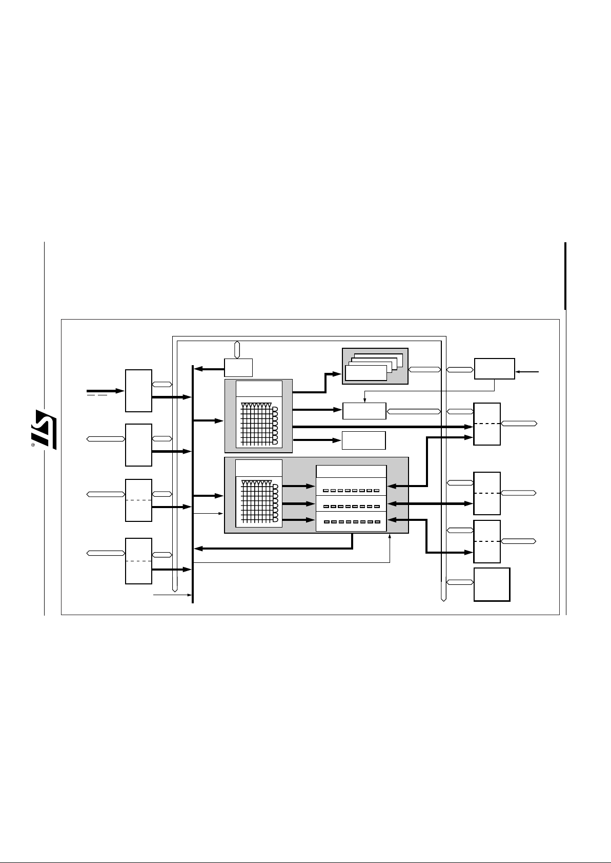
4.0
Zero-Power
Background
PSD4XX Family
4
PROG.
BUS
INTRF
ADIO
PORT
PROG.
PORT
PROG.
PORT
PORT
C
PROG.
PORT
PORT
D
CONTROL
RD, WR
AD0 – AD15
PC0 – PC7
PD0 – PD7
CLKIN
CLKIN
PAGE
REG.
ZPLD
INPUT
BUS
GLOBAL
CONFIG.
&
SECURITY
PORT
A
POWER
MANAGER
UNIT
VSTDBY
PA0 – PA7
PROG.
PORT
PORT
B
PB0 – PB7
PROG.
PORT
PORT
E
PE0 – PE7
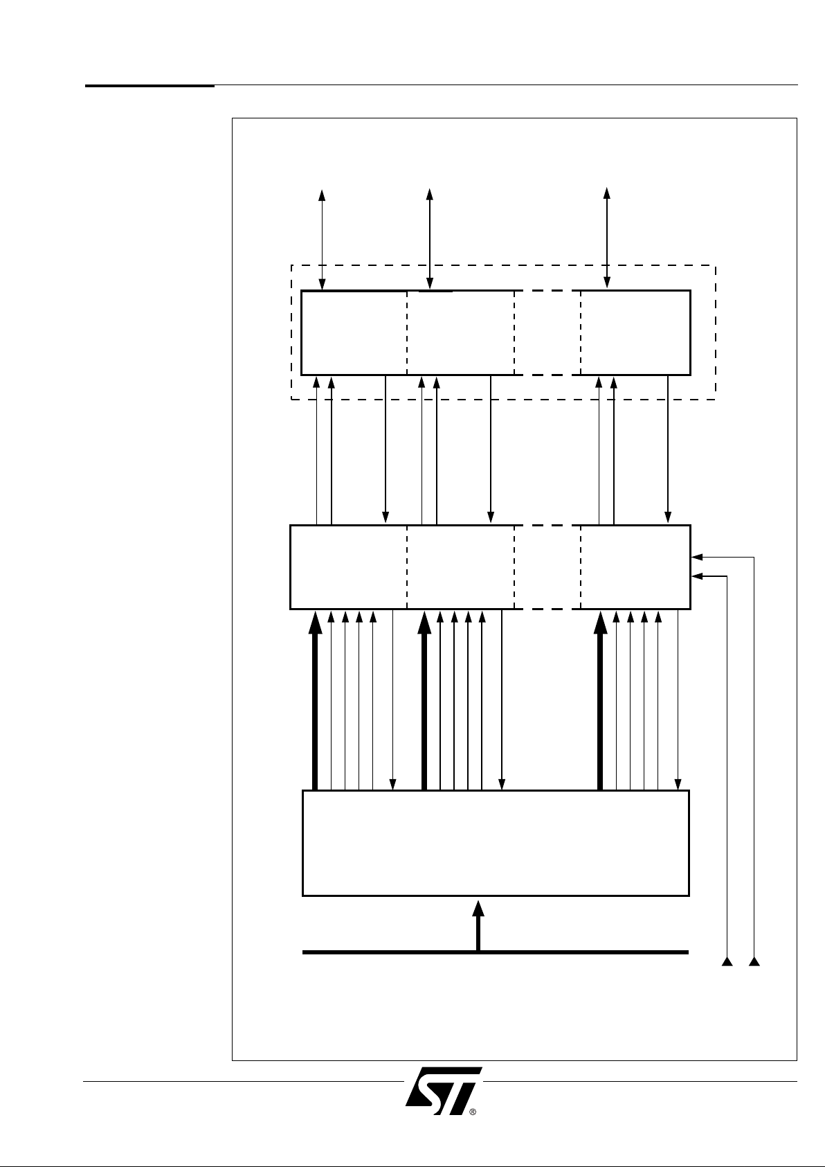
ADDRESS/DATA/CONTROL BUS
PORT A MACROCELLS
PORT B MACROCELLS
PORT E MACROCELLS
(NOTE 2)
27PT
(NOTE 1)
(NOTE 1)
80PT
11PT
CLKIN
256K– 1M BIT
EPROM
16 K BITS
SRAM
I/O
DECODER
EPROM
SELECTS
SRAM
SELECT
PERIPHERAL
SELECTS
MACROCELL FEEDBACK OR PORT INPUT
CSIOP
GENERAL PLD
(GPLD)
24 MACROCELLS
DECODE PLD
(DPLD)
NOTES: 1. ZPLD INPUT BUS
– A1 = 36 + CLOCK = 37 INPUTS
– A2 = 58 + CLOCK = 59 INPUTS
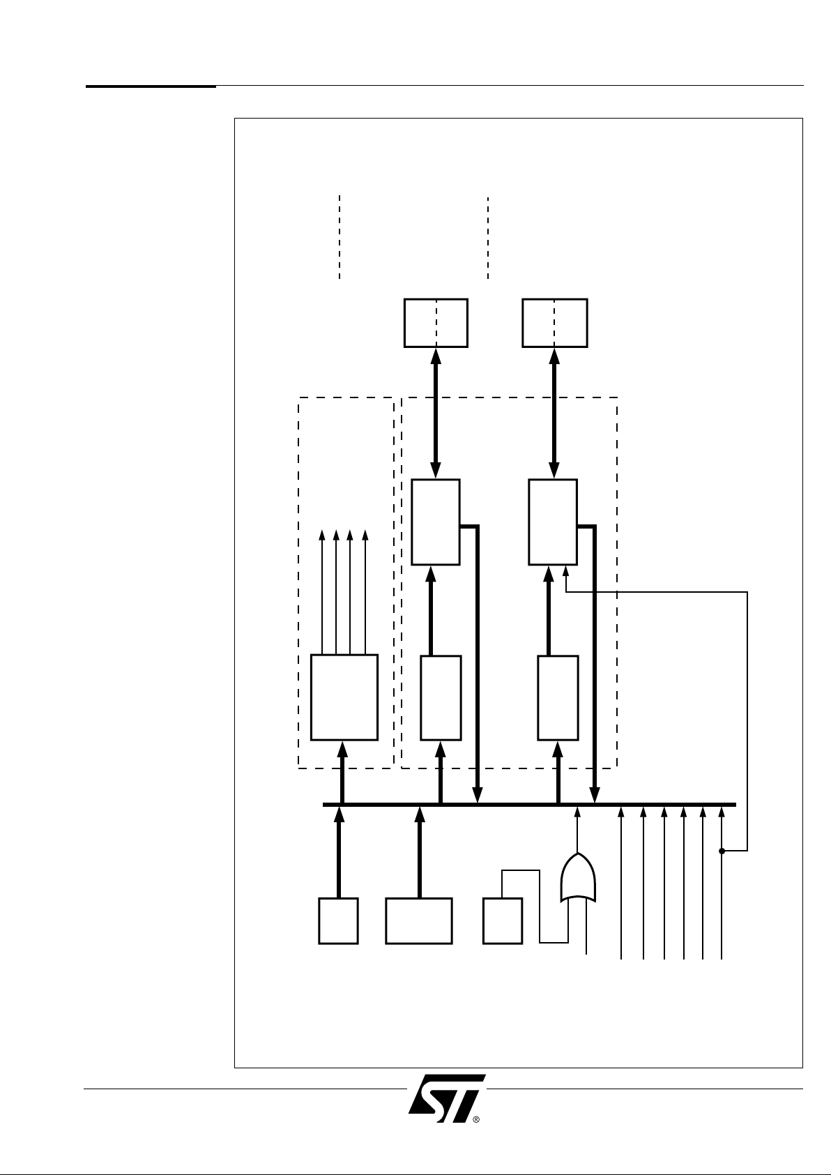
2. PORT E MACROCELLS AVAILABLE ON A2 VERSIONS ONLY.
Figure 1.
PSD4XX
Block Diagram
PSD4XX Family
5
5.0
Integrated
Power
Management
TM
Operation
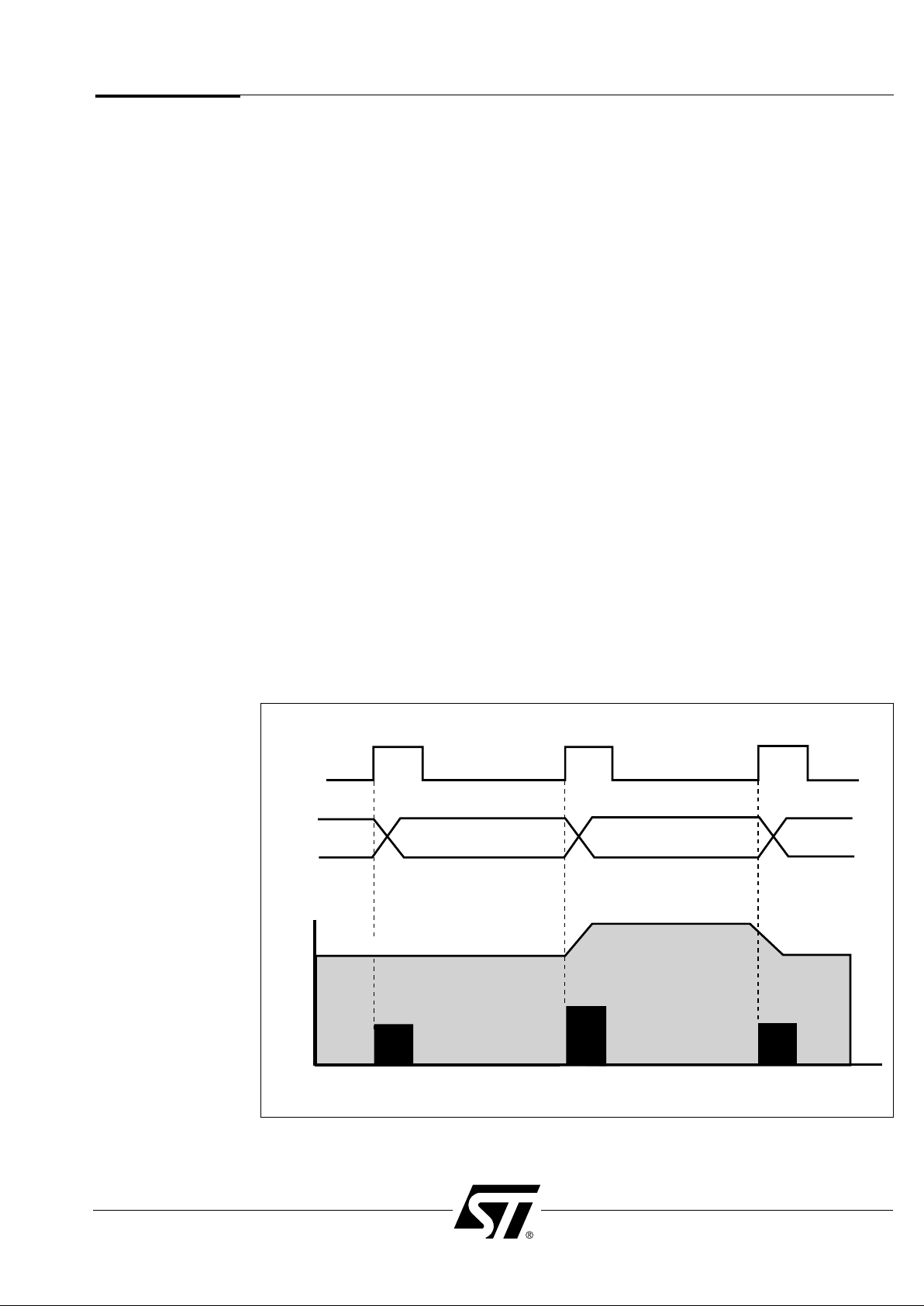
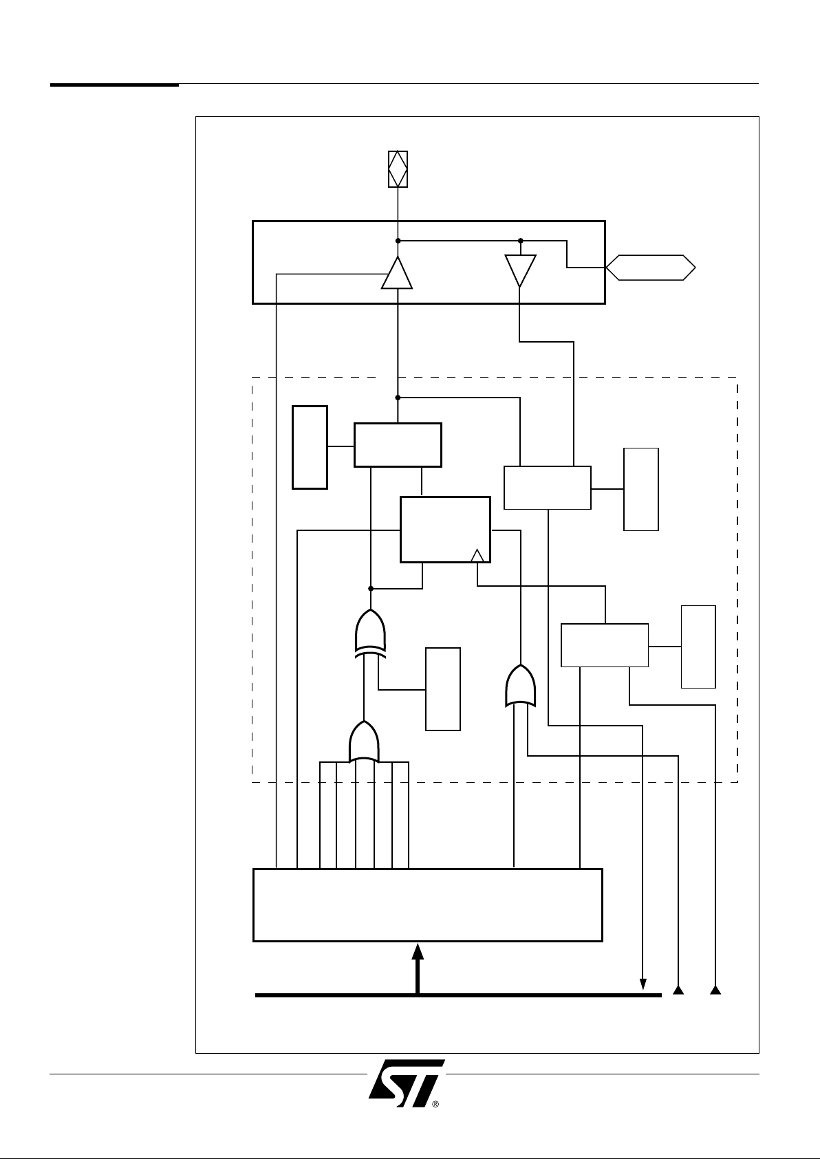
Upon each address or logic input change to the ZPSD, the device powers up from low
power standby for a short time. Then the ZPSD consumes only the necessary power to
deliver new logic or memory data to its outputs as a response to the input change. After the
new outputs are stable, the ZPSD latches them and automatically reverts back to standby
mode. The ICCcurrent flowing during standby mode and during DC operation is identical
and is only a few microamperes.
The ZPSD automatically reduces its DC current drain to these low levels and does not
require controlling by the CSI (Chip Select Input). Disabling the CSI pin unconditionally
forces the ZPSD to standby mode independent of other input transitions.
The only significant power consumption in the ZPSD occurs during AC operation.
The ZPSD contains the first architecture to apply zero power techniques to memory and
logic blocks.
Figure 2 compares ZPSD Zero-power operation to the operation of a discrete solution.
A standard microcontroller (MCU) bus cycle usually starts with an ALE (or AS) pulse and
the generation of an address. The ZPSD detects the address transition and powers up for a
short time. The ZPSD then latches the outputs of the PAD, EPROM and SRAM to the new
values. After finishing these operations, the ZPSD shuts off its internal power, entering
standby mode. The time taken for the entire cycle is less than the ZPSD’s “access time.”
The ZPSD will stay in standby mode if inputs do not change between bus cycles. In an
alternate system implementation using discrete EPROM, SRAM, and other discrete
components, the system will consume operating power during the entire bus cycle. This is
because the chip select inputs on the memory devices are usually active throughout the
entire cycle. The AC power consumption of the ZPLD may be calculated using the
composite frequency of the MCU address and control signals, as well as any other logic
inputs to the ZPLD.
NOTE: The ZPSD4XX is rated for lower standby current (ISB) than the PSD4XX.
ALE
DISCRETE EPROM, SRAM & LOGIC
ADDRESS
EPROM
ACCESS
SRAM
ACCESS
EPROM
ACCESS
I
CC
ZPSD
ZPSD
ZPSD
TIME
Figure 2. Zero-Power Operation vs. Discrete Implementation
PSD4XX Family
6
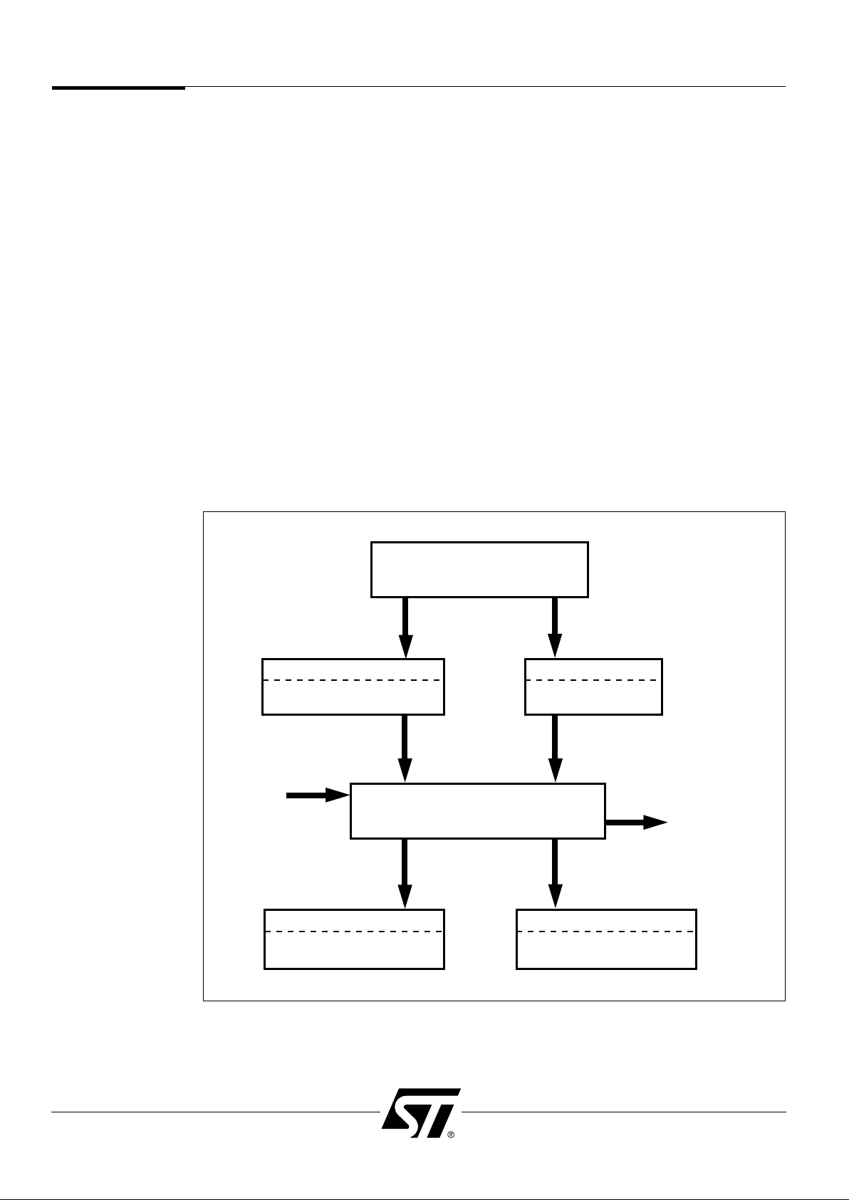
Figure 3. PSDsoft Development Tools
PSDsilos III™
SILOSIII
CHIP SIMULATION
PSD Programmer
PSDpro/MagicPro
®
CHIP PROGRAMMING
PSD Compiler
(ZPLD FITTING, ADDRESS TRANSLATION)
PSDabel™
ZPLD DESCRIPTION
(STATE MACHINE, DECODING)
PSDsoft
Development Software
PSD Configuration
CHIP CONFIGURATION
THIRD PARTY
PROGRAMMERS
CODE FILE
Shown in Figure 3 (below) is the software design flow for a PSD4XX device.
PSDsoft—ST’s software development suite—is used throughout the design phase. You
start with a design file that is written in PSDabel—a high-level hardware description
language (HDL). Before you compile your design, you must also configure the PSD4XX so
it knows what signals to expect from your microprocessor and what pre-runtime options
should be set (such as the security bit).
Once you have a design file and have configured the device, you are ready to run the Fitter
and Address Translator. The Fitter accepts input from PSDabel and PSD Configuration,
synthesizes this user logic and configuration, and fits the design to the PSD silicon. The
Address Translator process allows the user to map the MCU firmware from a crosscompiler (in Intel HEX or S-Record format) into the NVM memory blocks within the PSD. As
a result, the MCU firmware is merged with the logic and configuration definition of the PSD.
The output of the Address Translator and the Fitter is the required object file that is used by
a programmer to program the PSD device. The object file includes chip configuration, the
PLD fusemap, and MCU firmware information.
PSDsilosIII is an optional program that provides functional chip-level simulation of the
PSD4XX. PSDsoft automatically creates files for input to the simulator. These files convey
relevant design information to the simulator. As a result, the user only has to create a
stimulus file since all of the signals and node names are taken from the design file.
6.0
Design Flow
PSD4XX Family
7
7.0
PSD4XX
Family
There are 12 unique devices in the PSD4XX family. The part classifications are based on
ZPLD configuration and size, EPROM size, and data bus width. The features of each part
are listed in Table 1. See the ordering information section at the end of this document.
Part Bus
DPLD + GPLD
I/O
PMU
EPROM SRAM
# Bit
Inputs Product Registered
Pins K Bit K Bit
Terms Macrocells
401A1 x8/x16 37 113 8 40 Yes 256 16
411A1 x8 37 113 8 40 Yes 256 16
402A1 x8/x16 37 113 8 40 Yes 512 16
412A0 x8 37 113 8 40 Yes 512 –
412A1 x8 37 113 8 40 Yes 512 16
403A1 x8/x16 37 113 8 40 Yes 1024 16
413A1 x8 37 113 8 40 Yes 1024 16
401A2 x8/x16 59 126 24 40 Yes 256 16
411A2 x8 59 126 24 40 Yes 256 16
402A2 x8/x16 59 126 24 40 Yes 512 16
412A2 x8 59 126 24 40 Yes 512 16
403A2 x8/x16 59 126 24 40 Yes 1024 16
413A2 x8 59 126 24 40 Yes 1024 16
Table 1. PSD4XX Product Matrix
NOTE: PMU = Power Management Unit.
PSD4XX Family
8
Pin Name Pin Function Type Function Descriptions
ADIO0 – ADIO15 Address/data bus I/O 1. Address/data bus, multiplexed
bus mode
2. Address bus, non-multiplexed
bus mode
RD Multiple Names I Multiple functions
1. Read 1. Read signal
2. E 2. E signal (Clock)
3. DS 3. Data strobe signal
4. LDS 4. Low byte data strobe
WR Multiple Names I Multiple functions
1. WR 1. Write signal
2. R/W 2. Read-write signal
3. WRL 3. Low byte write signal
CSI Chip Select Input I Active low, select PSD4XX
standby mode if high.
RESET Reset Input I Reset I/O ports, ZPLD/macrocells,
and Configuration Registers.
Active low.
CLKIN Input clock I Clock input to ZPLD macrocells,
ZPLD Array and APD counter.
Connect to ground if Clock Input
not used.
PA0 – PA7 I/O Port A I/O Multiple functions
1. I/O port
2. ZPLD/macrocell I/O port
3. Latched address outputs
(PA0 – PA7) → (A0 – A7)
4. High address inputs (A16 – A23)
PB0 – PB7 I/O Port B I/O Multiple functions
1. I/O port
2. ZPLD/macrocell I/O port
3. Latched address outputs
(PB0–PB7) → (A0–A7) or (A8–A15)
PC0 – PC7 I/O Port C I/O Multiple functions
CMOS 1. I/O port
or 2. ZPLD input port*
OD 3. Latched address outputs
(PC0 – PC7) → (A0–A7)
4. Data Port (D0 – D7,
non-multiplexed bus)
PD0 – PD7 I/O Port D I/O Multiple functions
CMOS 1. I/O port
or 2. ZPLD input port*
OD 3. Latched address outputs
(PD0–PD7) → (A0–A7) or (A8–A15)
4. Data Port (D8–D15,
non-multiplexed bus)
8.0
Table 2.
PSD4XX Pin
Descriptions
The following table describes the pin names and pin functions of the PSD4XX. Pins that
have multiple names and/or functions are defined by user configuration.
*Available only in PSD4XXA2 and ZPSD4XXA2 Series.
PSD4XX Family
9
Pin Name Pin Function Type Function Descriptions
PE0 Port PE, pin 0 I/O Multiple functions
1. BHE 1. High byte enable, 16 bit data
2. PSEN 2. Read program memory, 8031 signal
3. WRH 3. Write high data byte
4. UDS 4. Upper Data Strobe
5. SIZ0 5. Byte enable, 68300 signal
6. PE0 6. I/O pin
7. PE0 7. ZPLD I/O pin
8. PE0 8. Latched Address Out – A0
PE1 Port PE, pin 1 I/O Multiple functions
1. ALE 1. Address strobe
2. PE1 2. I/O pin
3. PE1 3. ZPLD I/O pin
4. PE1 4. Latched Address Out – A1
PE2 Port PE, pin 2 Multiple functions
1. PE2 I/O 1. I/O pin
2. PE2 2. ZPLD I/O pin*
3. PE2 3. Latched Address Out – A2
PE3 Port PE, pin 3 Multiple functions
1. PE3 I/O 1. I/O pin
2. PE3 2. ZPLD I/O pin*
3. PE3 3. Latched Address Out – A3
PE4 Port PE, pin 4 Multiple functions
1. PE4 I/O 1. I/O pin
2. PE4 2. ZPLD I/O pin*
3. PE4 3. Latched Address Out – A4
PE5 Port PE, pin 5 Multiple functions
1. PE5 I/O 1. I/O pin
2. PE5 2. ZPLD I/O pin*
3. PE5 3. Latched Address Out – A5
PE6 Port PE, pin 6 Multiple functions
1. PE6 I/O 1. I/O pin
2. PE6 2. ZPLD I/O pin*
3. PE6 3. Latched Address Out – A6
PE7 Port PE, pin 7 Multiple functions
1. APD CLK 1. Automatic Power Down Clock Input
2. PE7 I/O 2. I/O pin
3. PE7 3. ZPLD I/O pin*
4. PE7 4. Latched Address Out – A7
Vstdby Vstdby
I
SRAM power pin for standby
operation (battery backup)
V
CC
V
CC
IV
CC
power pin
GND GND I Ground pin
8.0
Table 2.
PSD4XX Pin
Descriptions
(Cont.)
*Available only in PSD4XXA2 and ZPSD4XXA2 Series.

PSD4XX Family
10
9.0
The PSD4XX
Architecture
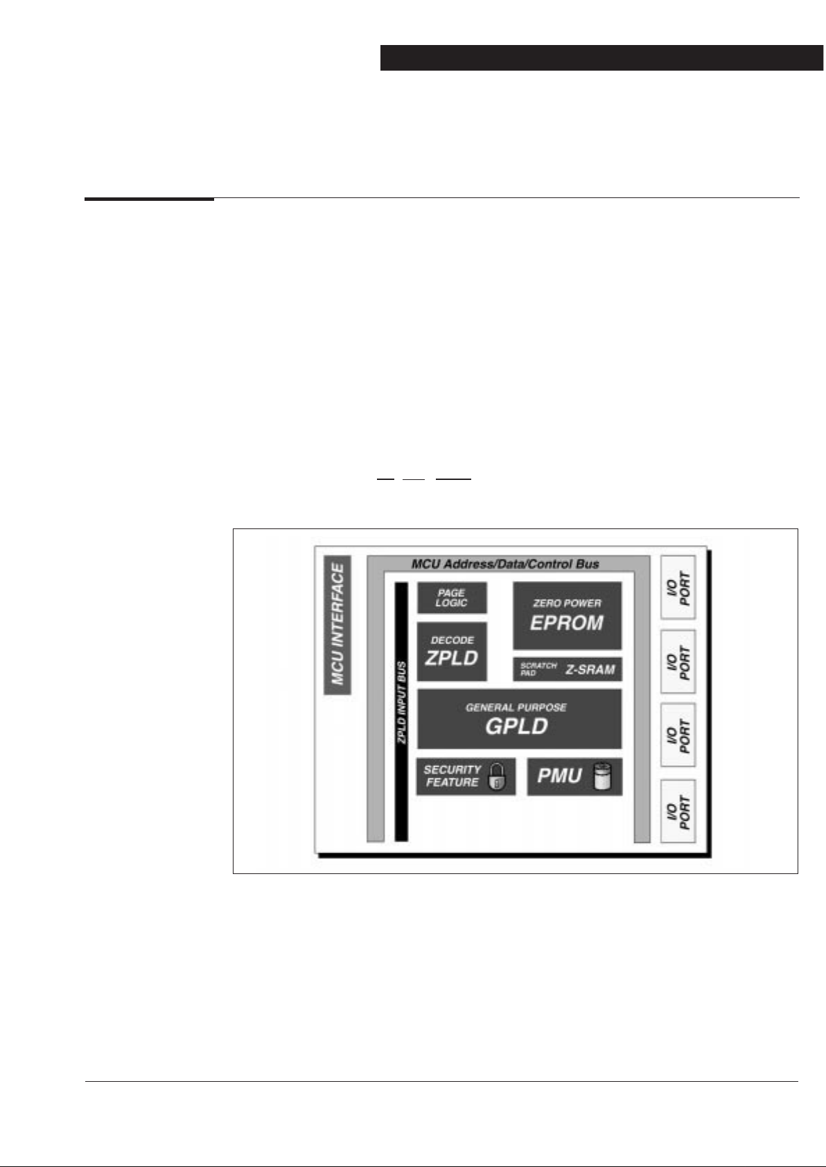
PSD4XX consists of five major functional blocks:
❏
ZPLD Blocks
❏
Bus Interface
❏
I/O Ports
❏
Memory Block
❏
Power Management Unit
The functions of each block are described in the following sections. Many of the blocks
perform multiple functions, and are user configurable. The chip configurations are specified
by the user in the PSDsoft Development Software. Other configurations are specified by
setting up the appropriate bits in the configuration registers during run time.
9.1 The ZPLD Block
The PSD4XX series devices provide two ZPLD configurations. The ZPLD in the
PSD4XXA1 devices has 8 registered macrocells, 8 combinatorial macrocells, and up to 113
product terms.
The PSD4XXA2 has a full function ZPLD with 24 registered macrocells and up to 126
product terms.
9.1.1 The PSD4XXA1 ZPLD Block
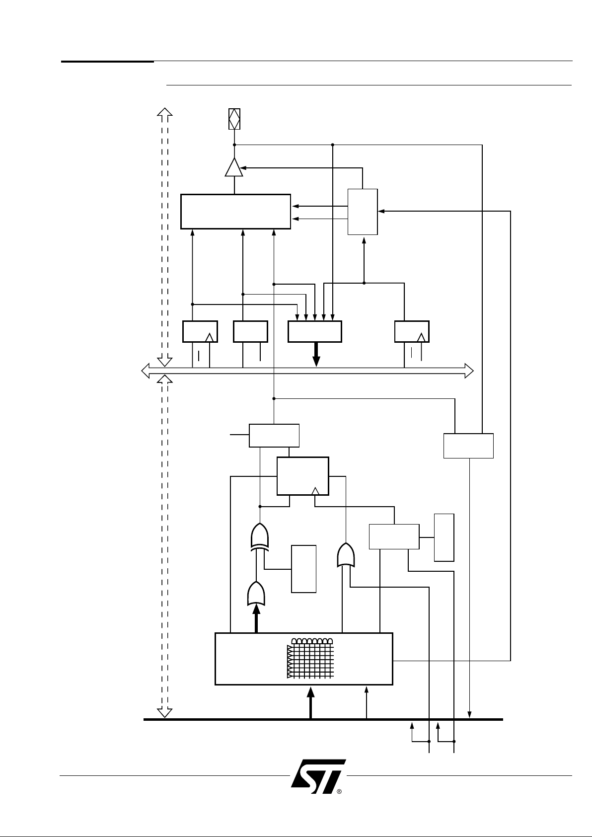
Key Features
❏ 2 Embedded ZPLD devices
❏ 8 registered and 8 combinatorial macrocells
❏ Combinatorial/registered outputs
❏ Maximum 113 product terms
❏ Programmable output polarity
❏ User configured register clear/preset
❏ User configured register clock input
❏ 37 Inputs
❏ Accessible via 16 I/O pins
❏ Power Saving Mode
❏ UV-Erasable
General Description
The ZPLD block has 2 embedded PLD devices:
❏
DPLD
The Address Decoding PLD, generating select signals to internal I/O or memory blocks.
❏
GPLD
The General Purpose PLD provides 8 registered and combinatorial programmable
macrocells for general or complex logic implementation; dedicated to user application.
Figure 4 shows the architecture of the ZPLD. The PLD devices all share the same input
bus. The true or complement of the 37 input signals are fed to the programmable
AND-ARRAY. Names and sources of the input signals are shown in Table 3. The PB
signals, depending on user configuration, can either be macrocell feedbacks or inputs from
Port B.
PSD4XX Family
11
Figure 4. ZPLD Block Diagram
PAGE
REG.
ADIO
PORT
PMU
CSI
RD/E/DS
PE1 (PSEN/BHE)
PE0 (ALE/AS)
WR/R_W
RESET
CLKIN
PGR0 – 3
A8 – A15
A0, A1
AND
ARRAY
AND
ARRAY
DPLD
ES0 – ES3
RS0
CSIOP
PSEL0 – PSEL1
8 I/O
MACROCELLS
PA
8 I/O
MACROCELLS
PB
(NOTE 1)
80 PT
PB0 – PB7
PA0 – PA7
PROG.
PORT
PORT
A
PROG.
PORT
PORT
B
DPLD
GPLD
ZPLD INPUT
BUS
(DECODING PLD)
(GENERAL
PURPOSE PLD)
NOTE 1: A1 = 25 PT ON PORT A
A2 = 27 PT ON PORT A
The PSD4XX
Architecture
(cont.)
PSD4XX Family
12
Signal Name From
PA0 – PA7 Port A inputs or Macrocell PA feedback
PB0 – PB7 Port B inputs or Macrocell PB feedback
PE0 – PE1 Port E inputs (signals ALE, PSEN/BHE)
PGR0 – PGR3 Page Mode Register
A8 – A15, A0, A1 MCU Address Lines
RD/E/DS MCU bus signal
WR/R_W MCU bus signal
CLKIN Input Clock
RESET Reset input
CSI CSI input (ORed with power down from PMU)
Table 3. ZPLD Input Signals
9.0
The PSD4XX
Architecture
(cont.)
9.1.1.1 The DPLD
The DPLD is used for internal address decoding generating the following eight chip select
signals:
❏
ES0 – ES3
EPROM selects, block 0 to block 3
❏
RS0
SRAM block select
❏
CSIOP
I/O Decoder chip select
❏
PSEL0 – PSEL1
Peripheral I/O mode select signals
The I/O Decoder enabled by the CSIOP generates chip selects for on-chip registers or I/O
ports based on address inputs A[7:0].
As shown in Figure 4, the DPLD consists of a large programmable AND ARRAY. There are
a total of 37 inputs and 8 outputs. Each output consists of a single product term. Although
the user can generate select signals from any of the inputs, the select signals are typically
a function of the address and Page Register inputs. The select signals are defined by the
user in the ABEL file (PSDabel).
The address line inputs to the DPLD include A0, A1 and A8 – A15. If more address lines
are needed, the user can bring in the lines through Port A to the DPLD.

PSD4XX Family
13
9.1.1.2 The GPLD
The structure of the General Purpose PLD consists of a programmable AND ARRAY
and 2 sets of I/O Macrocells. The ARRAY has 37 input signals, same as the DPLD.
From these inputs, “ANDed” functions are generated as product term inputs to the
macrocells. The I/O Macrocell sets are named after the I/O Ports they are linked to,
e.g., the macrocells connected to Port B are named PB Macrocells. The PB macrocells
are registered macrocells with D-type flip-flops, where PA consists of combinatorial
macrocells.
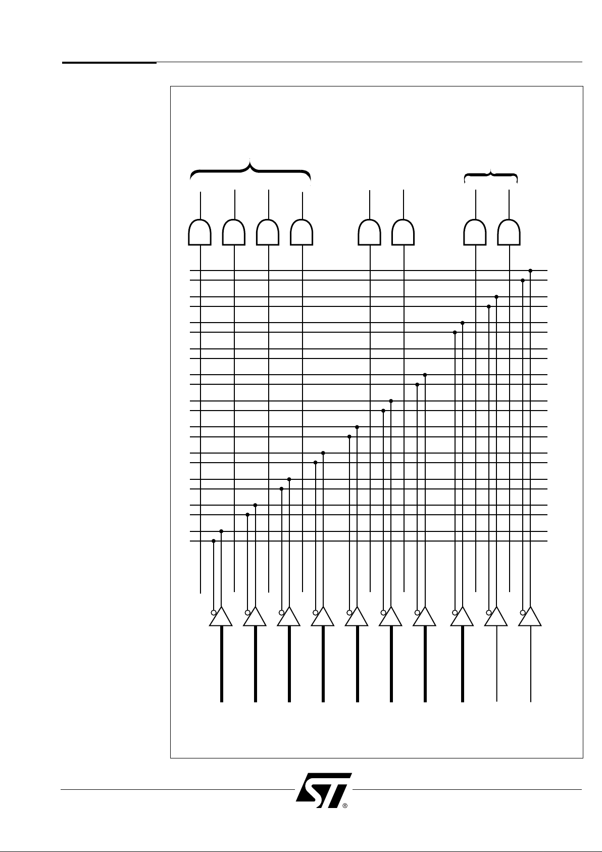
9.1.1.3 TPA Macrocell Structure
Figure 5 shows the PA Macrocell block, which consists of 8 identical combinatorial
macrocells. Each macrocell output can be connected to its own I/O pin on Port A.
There is one user programmable global product term that is output from the GPLD’s
AND ARRAY which is shared by all the macrocells in Port A:
❏ PA.OE
Enable or tri-state Port A output pins
The circuit of a PA Macrocell is shown in Figure 6. There are 4 product terms from the
GPLD’s AND ARRAY as inputs to the macrocell. Users can select the polarity of the
output, and configure the macrocell to operate as:
❏ GPLD Input
Use Port A pin as dedicated input
❏ GPLD Output
Use Port A pin as dedicated output
9.0
The PSD4XX
Architecture
(cont.)
PSD4XX Family
14
Figure 5. DPLD Logic Array
PA0 – PA7
(8)
(8)
(2)
(10)
(3)
(1)
(1)
(INPUTS)
PB0 – PB7
PE0 – PE1
(4)
PGR0 – PGR3
A8 – A15, A0, A1
CSI, CLKIN
RESET
RD/E/DS
WR/R_W
ES0
ES1
ES2
ES3
RS0
CSIOP
PSEL0
PSEL1
4 EPROM
BLOCK
SELECTS
RAM SELECT
I/O DECODER
SELECT
PERIPHERAL
I/O SELECTS
DPLD INPUTS = 37
DPLD OUTPUTS = 8
(ALE, PSEN/BHE)
9.0
The PSD4XX
Architecture
(cont.)
PSD4XX Family
15
Figure 6. PA Macrocell Block Diagram
AND ARRAY
MC0 PA0
MC1 PA1
MC7 PA7
MACRO. OUT
PA0–INPUT
MACRO. OUT
PA1–INPUT
MACRO. OUT
PA7–INPUT
PT
[
2:0
]
PA0
PT
[
2:0
]
PA1
PT
[
2:0
]
PA7
PA.OE
PORT A I/O CELLS
PA MACROCELL
ZPLD
BUS
9.0
The PSD4XX
Architecture
(cont.)
PSD4XX Family
16
Figure 7. PA Macrocell
PT
PT
PT
PT
AND
ARRAY
POLARITY
SELECT
PLD–IN
SELECT
MUX
PA.OE
PT0
PT1
PT2
PAi
NOTE: i = 7 TO 0
MACRO.OUT
I/O PIN
PAi
PORT A
INTERNAL
ADDRESS/DATA
BUS
PAi–INPUT
ZPLD
BUS
9.0
The PSD4XX
Architecture
(cont.)

PSD4XX Family
17
9.1.1.4 Port B Macrocell Structure
Figure 7 shows the PB Macrocell block, which consists of 8 identical macrocells. Each
macrocell output can be connected to its own I/O pin on Port B. The two inputs, CLKIN and
MACRO-RST, are used as clock and clear inputs to all the macrocells. The CLKIN comes
directly from the CLKIN input pin. The MACRO-RST is the same as the Reset input pin
except it is user configurable.
The circuit of a PB Macrocell is shown in Figure 8. There are 10 product terms from the
GPLDs AND ARRAY as inputs to the macrocell. Users can select the polarity of the output,
and configure the macrocell to operate as:
❏ Registered Output
Select output from D flip flop.
❏ Combinatorial Output
Select output from OR gate.
❏ GPLD Input
Use Port B pin as dedicated input.
❏ GPLD Output
Use Port B pin as dedicated output.
❏ GPLD I/O
Use Port B pin as bidirectional pin.
❏ Macrocell Feedback
Register feedback for state machine implementations or expander feedback from the
combinatorial output, to possibly expand the number of product terms available to
another macrocell.
In case of "Buried Feedback", where the output of the macrocell is not connected to
a Port B pin, Port B can be configured to perform other user defined I/O functions.
Each D flip flop in the macrocells has its own dedicated asynchronous clear, preset and
clock input. The signals are defined as follow:
❏ PRESET
Active only if defined by a product term (PBi.PR)
❏ CLEAR
Two selectable inputs: Reset input and/or user defined product term (PBi.RE)
❏ CLK
Two selectable inputs – CLKIN input or user defined product term (PBi.CLK).
The macrocell is operated in Synchronous Mode if the clock input is CLKIN, and is in
Asynchronous Mode if the clock is a product-term clock defined by the user.
Figure 9 shows the input/output path of a PB macrocell to the Port pin with which it is
associated. If the Port pin is specified as a PB output pin in the PSDsoft, the MUX in the I/O
Port Cell selects the PB Macrocell as an output of the Port pin. The output enable signal to
the buffer in the I/O cell can be controlled by a product term from the AND Array.
If the Port pin is specified as a ZPLD input pin, the MUX in the PB Macrocell selects the
Port input signal to be one of the 61 signals in the ZPLD Input Bus.
9.0
The PSD4XX
Architecture
(cont.)

PSD4XX Family
18
9.0
The PSD4XX
Architecture
(cont.)
9.1.1.5 The ZPLD Power Management
The ZPLD implements a Zero Power Mode, which provides considerable power savings
for low to medium frequency operations. To enable this feature, the ZPLD Turbo bit in the
Power Management Mode Register 0 (PMMR0) has to be turned off.
If none of the inputs to the ZPLD are switching for a time period of 90ns, the ZPLD puts
itself into Zero Power Mode and the current consumption is minimal. The ZPLD will
resume normal operation as soon as one or more of the inputs change state.
Two other features of the ZPLD provide additional power savings:
1. Clock Disable:
Users can disable the clock input to the ZPLD and/or macrocells,thereby reducing
AC power consumption.
2. Product Term Disable:
Unused product terms in the ZPLD are disabled by the PSDsoft Software
automatically for further power savings.
The ZPLD power configuration is described in the Power Management Unit section.
PSD4XX Family
19
Figure 8. PB Macrocell Block Diagram
AND ARRAY
MACRO .OUT
PB0 .OE
PB0 – INPUT
MACRO .OUT
PB1 .OE
PB1–INPUT
MACRO .OUT
PB7 .OE
PB7– INPUT
PTB0 –
[
0 . . 5
]
PB0 .PR
PB0 .RE
PB0 .OE
PB0 .CLK
PB0
PTB1 –
[
0 . . 5
]
PB1 .PR
PB1 .RE
PB1 .OE
PB1 .CLK
PB1
PTB7 –
[
0 . . 5
]
PB7 .PR
PB7 .RE
PB7 .OE
PB7 .CLK
PB7
CLKIN
MACRO – RST
PORT B I/O CELLS
PB MACROCELL
MC0
MC1
MC7
PB0
PB1
PB7
ZPLD
BUS
9.0
The PSD4XX
Architecture
(cont.)
PSD4XX Family
20
Figure 9. PB Macrocell
DQ
PTPTPTPTPTPTPT
PT
PT
PT
AND
ARRAY
POLARITY
SELECT
COMB/REG
SELECT
C
PR
MUX
PLD–IN
SELECT
MUX
CLK
SELECT
MUX
PBi
PBi .OE
PBi .PR
PT0
PT1
PT2
PT3
PT4
PT5
PBi .CLK
PBi .RE
MACRO–RST
CLKIN
MACRO . OUT
I/O PIN
PBi
PORT B
INTERNAL
ADDRESS/DATA
BUS
PBi– INPUT
ZPLD
BUS
9.0
The PSD4XX
Architecture
(cont.)
PSD4XX Family
21
Figure 10. PB Macrocell Input/Output Port
DQ
PSD4XX FIG. 5
AND
ARRAY
PT
POLARITY
SELECT
CL
CK
PR
CONTROL
CLK
SELECT
MUX
PT CLOCK
PT OUTPUT ENABLE (OE)
PT RESET
PTs
PT CLEAR
MACRO_RST
GLOBAL
CLOCK
PORT
PIN
COMB./REG.
SELECT
GPLD
MACROCELL
OUTPUT
MUX
MUX
MUX
PCR
DQ
WR
DIRECTION
REGISTER
DQ
WR
D
G
Q
ALE
PDR
PORT INPUT
INPUT
OUTPUT
ADDRESS
A[0-7]
OR
A[8-15]
GPLD
OUTPUT
GPLD MACROCELL I/O PORT CELL
INTERNAL
ADDRESS/DATA/CONTROL
BUS
ZPLD
INPUT
BUS
CLKIN
9.0
The PSD4XX
Architecture
(cont.)

PSD4XX Family
22
The PSD4XX
Architecture
(cont.)
9.1.2 The PSD4XXA2 ZPLD Block
Key Features
❏ 2 Embedded ZPLD devices
❏ 24 macrocells
❏ Combinatorial/registered outputs
❏ Maximum 126 product terms
❏ Programmable output polarity
❏ User configured register clear/preset
❏ User configured register clock input
❏ 59 Inputs
❏ Accessible via 24 I/O pins
❏ Power Saving Mode
❏ UV-Erasable
General Description
The ZPLD block has 2 embedded PLD devices:
❏
DPLD
The Address Decoding PLD, generating select signals to internal I/O or memory blocks.
❏
GPLD
The General Purpose PLD provides 24 programmable macrocells for general
or complex logic implementation; dedicated to user application.
Figure 11 shows the architecture of the ZPLD. The PLD devices all share the same
input bus. The true or complement of the 59 input signals are fed to the programmable
AND-ARRAY. Names and source of the input signals are shown in Table 4. The PA, PB, PE
signals, depending on user configuration, can either be macrocell feedbacks or inputs from
Port A, B or E.
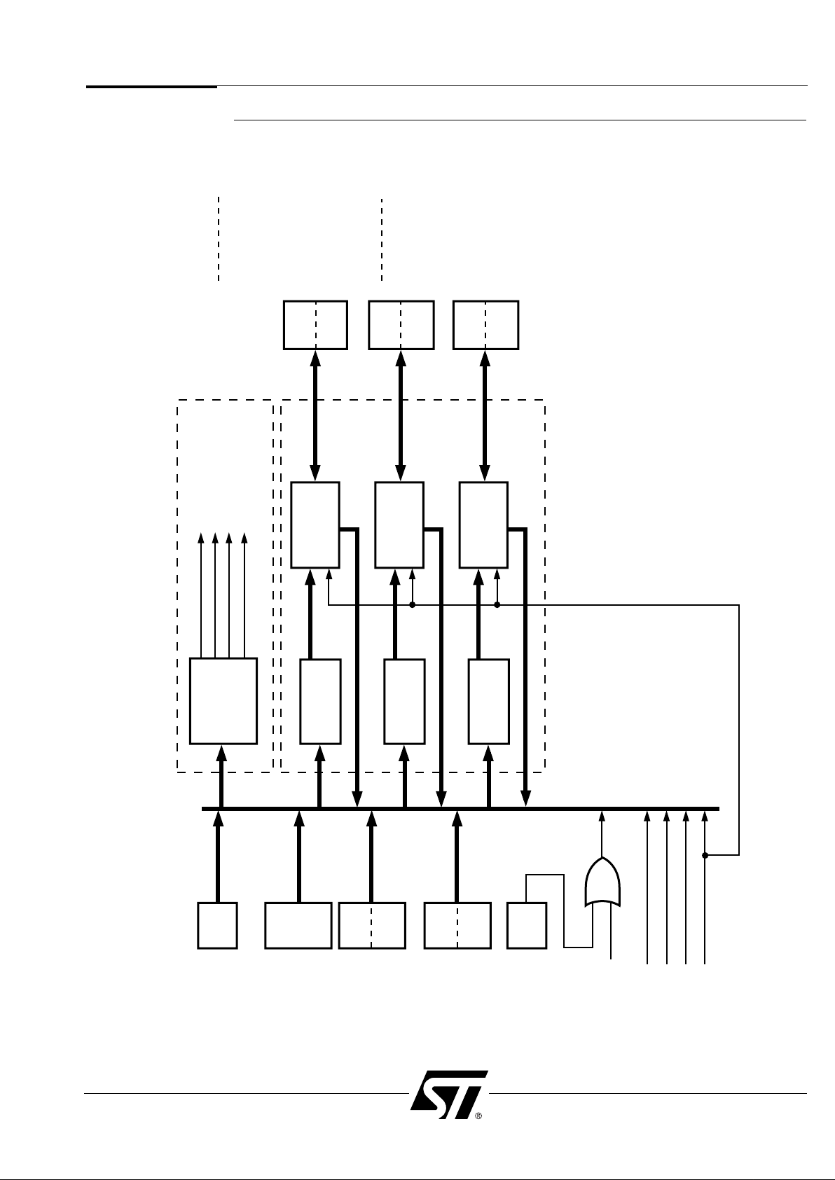
PSD4XX Family
23
PAGE
REG.
ADIO
PORT
PROG.
PORT
PORT
C
PROG.
PORT
PORT
D
PMU
CSI
RD/E/DS
WR/R_W
RESET
CLKIN
PGR0 – 3
A8 – A15
A0, A1
PC0 – PC7
PD0 – PD7
AND
ARRAY
AND
ARRAY
AND
ARRAY
DPLD
ES0 – ES3
RS0
CSIOP
PSEL0 – PSEL1
8 I/O
MACROCELLS
PA
8 I/O
MACROCELLS
PB
8 I/O
MACROCELLS
PE
27 PT
80 PT
11 PT
PE0 – PE7
PB0 – PB7
PA0 – PA7
PROG.
PORT
PORT
A
PROG.
PORT
PORT
B
PROG.
PORT
PORT
E
DPLD
GPLD
ZPLD INPUT
BUS
(DECODING PLD)
(GENERAL
PURPOSE PLD)
The PSD4XX
Architecture
(cont.)
Figure 11. PSD4XXA2 ZPLD Block Diagram
Signal Name From
PA0 – PA7 Port A inputs or Macrocell PA feedback
PB0 – PB7 Port B inputs or Macrocell PB feedback
PE0 – PE7 Port E inputs or Macrocell PE feedback
PC0 – PC7 Port C inputs
PD0 – PD7 Port D inputs
PGR0 – PGR3 Page Mode Register
A8 – A15, A0, A1 MCU Address Lines
RD/E/DS MCU bus signal
WR/R_W MCU bus signal
CLKIN Input Clock
RESET Reset input
CSI CSI input (ORed with power down from PMU)
PSD4XX Family
24
Table 4. ZPLD Input Signals
The PSD4XX
Architecture
(cont.)
9.1.2.1 The DPLD
The DPLD is used for internal address decoding generating the following eight chip select
signals:
❏
ES0 – ES3
EPROM selects, block 0 to block 3
❏
RS0
SRAM block select
❏
CSIOP
I/O Decoder chip select
❏
PSEL0 – PSEL1
Peripheral I/O mode select signals
The I/O Decoder enabled by the CSIOP generates chip selects for on-chip registers or I/O
ports based on address inputs A[7:0].
As shown in Figure 12, the DPLD consists of a large programmable AND ARRAY. There
are a total of 59 inputs and 8 outputs. Each output consists of a single product term.
Although the user can generate select signals from any of the inputs, the select signals are
typically a function of the address and Page Register inputs. The select signals are defined
by the user in the ABEL file (PSDabel).
The address line inputs to the DPLD include A0, A1 and A8 – A15. If more address lines
are needed, the user can bring in the lines through Port A to the DPLD.
PSD4XX Family
25
Figure 12. DPLD Logic Array
PA0 – PA7
(8)
(8)
(8)
(8)
(8)
(4)
(10)
(3)
(1)
(1)
(INPUTS)
PB0 – PB7
PE0 – PE7
PC0 – PC7
PD0 – PD7
PGR0 – PGR3
A8 – A15, A0, A1
CSI, CLKIN
RESET
RD/E/DS
WR/R_W
ES0
ES1
ES2
ES3
RS0
CSIOP
PSEL0
PSEL1
4 EPROM
BLOCK
SELECTS
RAM SELECT
I/O DECODER
SELECT
PERIPHERAL
I/O SELECTS
DPLD INPUTS : 59
DPLD OUTPUTS : 8
The PSD4XX
Architecture
(cont.)

PSD4XX Family
26
The PSD4XX
Architecture
(cont.)
9.1.2.2 The GPLD
The structure of the General Purpose PLD consists of a programmable AND ARRAY and
3 sets of I/O Macrocells. The ARRAY has 59 input signals, same as the DPLD. From these
inputs, “ANDed” functions are generated as product term inputs to the macrocells. The I/O
Macrocell sets are named after the I/O Ports they are linked to, e.g., the macrocells
connected to Port A are named PA Macrocells. The 3 sets of macrocells, PA, PB and PE,
are similar in structure and function.
Figure 13 shows the output/input path of a GPLD macrocell to the Port pin with which it is
associated. If the Port pin is specified as a GPLD output pin in PSDsoft, the MUX in the I/O
Port Cell selects the GPLD macrocell as an output of the Port pin. The output enable signal
to the buffer in the I/O cell can be controlled by a product term from the AND ARRAY.
If the Port pin is specified as a ZPLD input pin, the MUX in the GPLD macrocell selects the
Port input signal to be one of the 61 signals in the ZPLD Input Bus.
9.1.2.3 Port A Macrocell Structure
Figure 14 shows the PA Macrocell block, which consists of 8 identical macrocells.
Each macrocell output can be connected to its own I/O pin on Port A. There are 3 user
programmable global product terms output from the GPLD’s AND ARRAY which are
shared by all the macrocells in Port A:
❏ PA.OE
Enable or tri-state Port A output pins
❏ PA.PR
Preset D flip flop in the macrocells
❏ PA.RE
Reset/Clear D flip flop in the macrocells
Two other inputs, CLKIN and MACRO-RST, are used as clock and clear inputs to the D flip
flop. The CLKIN comes directly from the CLKIN input pin. The MACRO-RST is the same as
the Reset input pin except it is user configurable.
The circuit of a PA Macrocell is shown in Figure 15. There are 6 product terms from the
GPLD’s AND ARRAY as inputs to the macrocell. Users can select the polarity of the
output, and configure the macrocell to operate as:
❏ Registered Output
Select output from D flip flop
❏ Combinatorial Output
Select output from OR gate
❏ GPLD Input
Use Port A pin as dedicated input
❏ GPLD Output
Use Port A pin as dedicated output
❏ GPLD I/O
Use Port A pin as bidirectional pin
❏ Macrocell Feedback
Register feedback for state machine implementations or expander feedback from
the combinatorial output, to expand the number of product terms available to another
macrocell.
In case of "Buried Feedback", where the output of the macrocell is not connected to a
Port A pin, Port A can be configured to perform other user defined I/O functions.
The two global product terms assigned for asynchronous clear (PA.RE) and preset (PA.PR)
are mainly for proper PA Macrocell initialization. The macrocell flip-flop can also be cleared
during reset by MACRO-RST, if such an option is chosen. The clock source is always the
input clock CLKIN.
PSD4XX Family
27
Figure 13. GPLD Macrocell Input/Output Port
DQ
PSD4XX FIG. 18
AND
ARRAY
PT
POLARITY
SELECT
CL
CK
PR
CONTROL
CLK
SELECT
MUX
PT CLOCK
PT OUTPUT ENABLE (OE)
PT RESET
PTs
PT CLEAR
MACRO_RST
GLOBAL
CLOCK
PORT
PIN
COMB./REG.
SELECT
MACROCELL
OUTPUT
MUX
MUX
MUX
PCR
DQ
WR
DIRECTION
REGISTER
DQ
WR
D
G
Q
ALE
PDR
PORT INPUT
INPUT
OUTPUT
ADDRESS
A[0-7]
OR
A[8-15]
GPLD
OUTPUT
LATCH
QD
LATCH ONLY ON
PORT A
GPLD MACROCELL I/O PORT CELL
INTERNAL
ADDRESS/DATA/CONTROL
BUS
ZPLD
INPUT
BUS
 Loading...