


Low Cost Field Programmable Microcontroller Peripherals
FEATURES SUMMARY
■ Single Supply Voltage:
– 5 V±10% for PSD211R and ZPSD211R
– 2.7 to 5.5 V for ZPSD211RV
■ Up to 256 Kbit of EPROM
■ Input Latches
■ Programmable I/O ports
■ Programmable Security
PSD211R
ZPSD211R, ZPSD211RV
Figure 1. Packages
PLDCC44 (J)
CLDCC44 (L)
PQFP44 (M)
1/3January 2002

i
PSD211R Family
PSD211R ZPSD211R ZPSD211RV
Low Cost Microcontroller Peripherals
Table of Contents
1 Introduction...........................................................................................................................................................1
2 Notation ................................................................................................................................................................2
3 Key Features ........................................................................................................................................................4
4 PSD211R Family Feature Summary ....................................................................................................................5
5 Partial Listing of Microcontrollers Supported ........................................................................................................5
6 Applications ..........................................................................................................................................................5
7 ZPSD Background................................................................................................................................................5
7.1 Integrated Power ManagementTMOperation.............................................................................................6
8 Operating Mode....................................................................................................................................................9
9 Programmable Address Decoder (PAD)...............................................................................................................9
10 I/O Port Functions...............................................................................................................................................12
10.1 CSIOPORT Registers..............................................................................................................................12
10.2 Port A (PA0-PA7).....................................................................................................................................12
10.3 Port B (PB0-PB7).....................................................................................................................................14
10.4 Port C (PC0-PC2)....................................................................................................................................15
11 PSD Memory ......................................................................................................................................................16
11.1 EPROM....................................................................................................................................................16
11.2 Programming and Erasure.......................................................................................................................16
12 Control Signals ...................................................................................................................................................16
12.1 ALE or AS................................................................................................................................................17
12.2 WR or R/W...............................................................................................................................................17
12.3 RD/E........................................................................................................................................................17
12.4 PSEN.......................................................................................................................................................17
12.5 A19/CSI ...................................................................................................................................................17
12.6 Reset Input ..............................................................................................................................................18
13 Program/Data Space and the 8031....................................................................................................................20
14 Systems Applications..........................................................................................................................................21
15 Security Mode.....................................................................................................................................................23
16 Power Management............................................................................................................................................23
16.1 CSI Input..................................................................................................................................................23
16.2 CMiser Bit................................................................................................................................................23
16.3 Turbo Bit (ZPSD Only).............................................................................................................................24
16.4 Number of Product Terms in the PAD Logic............................................................................................24
16.5 Composite Frequency of the Input Signals to the PAD Logic..................................................................25
16.6 Loading on I/O Pins.................................................................................................................................26
17 Calculating Power...............................................................................................................................................27
18 Specifications......................................................................................................................................................30
18.1 Absolute Maximum Ratings.....................................................................................................................30
18.2 Operating RAnge.....................................................................................................................................30
18.3 Recommended Operating Conditions......................................................................................................30
18.4 Pin Capacitance.......................................................................................................................................30
18.5 AC/DC Characteristics – PSD211R/ZPSD211R (All 5 V devices)...........................................................31
18.6 AC/DC Characteristics – PSD211RV (3 V devices only).........................................................................32
18.7 Timing Parameters – PSD211R/ZPSD211R (All 5 V devices)................................................................33
18.8 Timing Parameters – ZPSD211RV (3 V devices only)............................................................................34
18.9 Timing Diagrams for PSD211R Parts.....................................................................................................36
18.10 AC Testing...............................................................................................................................................39

ii
PSD211R Family
PSD211R ZPSD211R ZPSD211RV
Low Cost Microcontroller Peripherals
Table of Contents
(cont.)
19 Pin Assignments.................................................................................................................................................40
20 Package Information...........................................................................................................................................41
21 Package Drawings..............................................................................................................................................42
22 PSD211R Ordering Information..........................................................................................................................45
22.1 Selector Guide.........................................................................................................................................45
22.2 Part Number Construction.......................................................................................................................46
22.3 Ordering Information................................................................................................................................46
23 Data Sheet Revision History...............................................................................................................................47
Sales Reps .........................................................................................................................................................48
1
1.0
Introduction
Programmable Peripheral
PSD211R
Field-Programmable Microcontroller Peripheral
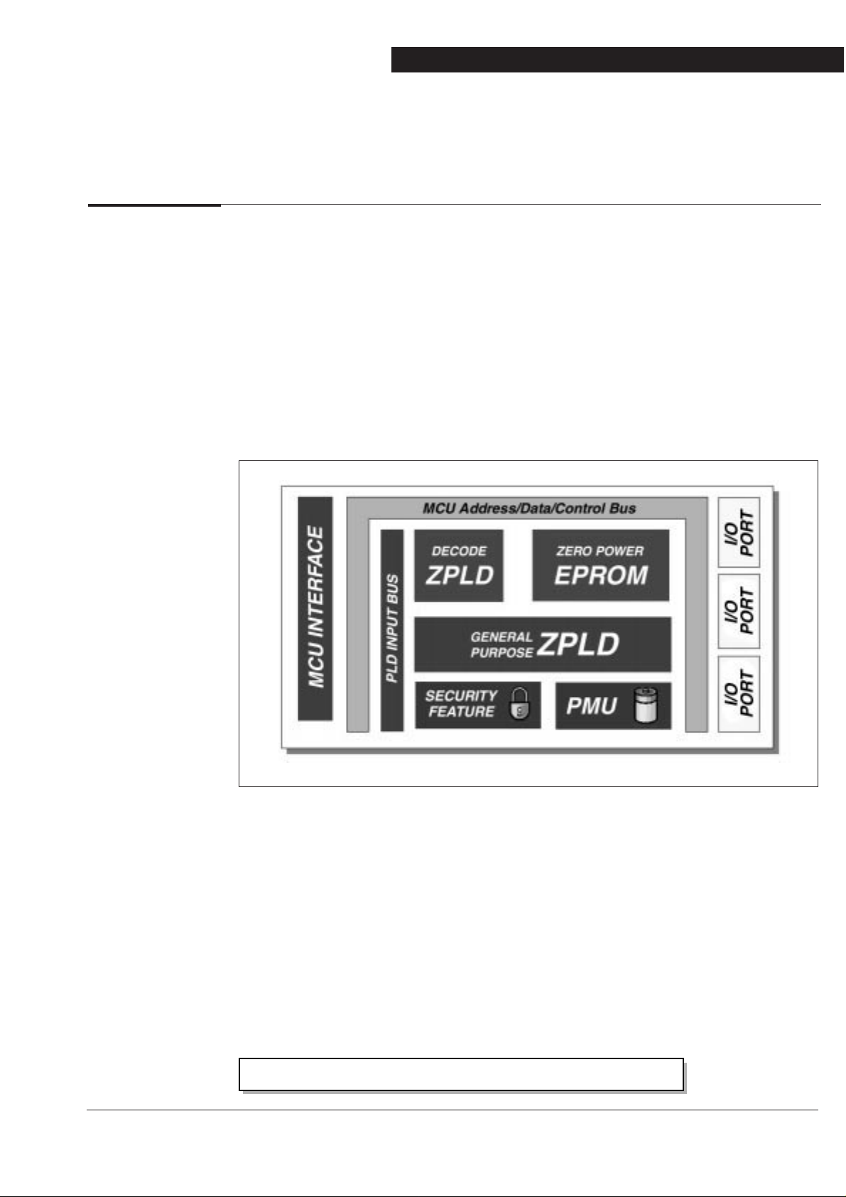
The low cost PSD211R family integrates high-performance and user-configurable blocks of
EPROM and programmable logic into one part. The PSD211R products also provide a
powerful microcontroller interface that eliminates the need for external “glue logic”. The
part’s integration, small form factor, low power consumption, and ease of use make it the
ideal part for interfacing to virtually any microcontroller.
The major functional blocks of the PSD211R include:
• Two programmable logic arrays
• 256 Kb of EPROM
• Input latches
• Programmable I/O ports
• Programmable security
The PSD211R family architecture (Figure 1) can efficiently interface with, and enhance,
almost any 8-bit multiplexed microcontroller system. This solution provides microcontrollers
the following:
• Chip-select logic, control logic, and latched address signals that are otherwise
implemented discretely
• Port expansion (reconstructs lost microcontroller I/O)
• An EPROM (with security)
• Compatible with 8031-type architectures that use separate Program and Data Space.
Updated March 1, 1999. See page 47.
PSD211R Family
2
2.0
Notation
1.0
Introduction
(Cont.)
The PSD211R I/O ports can be used for:
• Standard I/O ports
• Programmable chip select outputs
• Address inputs
• Demultiplexed address outputs.
Implementing your design has never been easier than with PSDsoft—WSI’s software
development suite. Using PSDsoft, you can do the following:
• Configure your PSD211R to work with virtually any 8-bit microcontroller
• Specify what you want implemented in the programmable logic using a high-level
Hardware Description Language (HDL)
• Simulate your design
• Download your design to the part using a programmer.
Throughout this data sheet, references are made to the PSD211R. In most cases, these
references also cover the ZPSD211R and ZPSD211RV products. Exceptions will be noted.
Also, references to the ZPSD211R will also cover the low-voltage ZPSD211RV. (Again,
exceptions will be noted.) Use the following table to determine what references cover which
product versions:
Reference PSD211R ZPSD211R ZPSD211RV
PSD211R or PSD X X X
PSD211R only X
Non-ZPSD X
ZPSD versions only X X
Non-V versions X X
V versions only or 3 V part only or
ZPSD211RV only
X
PSD211R Family
3
PROG.
PORT
EXP.
PORT
C
PC0–PC2
ES0
ES1
ES2
ES3
ES4
ES5
ES6
ES7
PROG.
CONTROL
SIGNALS
A19/CSI
RESET
WR/R/W
RD/E
ALE/AS
PSEN
PAD A
RESET
WR
ALE/AS
RD
PAD B
A11–A15
PROG.
PORT
EXP.
PORT
B
PB0–PB7
PROG.
PORT
EXP.
PORT
A
PA0–PA7
A19/CSI
RESET
ALE/AS
A19/CSI
A8–A10
WR
RD
ALE/AS
L
A
T
C
H
L
A
T
C
H
A8–A15
AD0–AD7
D0–D7
13 P.T.
27 P.T.
LOGIC
IN
EPROM
256Kb
A16–A18
CS8–CS10
CS0–CS7
A0–A7
CSIOPORT
PROG. CHIP
CONFIGURATION
Figure 1.
PSD211R Family
Architecture

PSD211R Family
4
3.0
Key Features
❏ Low cost programmable microcontroller peripheral
❏ 256Kb of UV EPROM with the following features:
• Configurable as 32 K x 8
• Divided into eight equally-sized mappable blocks for optimized address mapping
• As fast as 70 ns access time, which includes address decoding
❏ 19 I/O pins that can be individually configured for :
• Microcontroller I/O port expansion
• Programmable Address decoder (PAD) I/O
• Latched address output
❏ Two Programmable Arrays (PAD A and PAD B) replace your discrete PLD or decoder
and have the following features:
• Up to 13 Inputs and 24 outputs
• 36 Product terms (9 for PAD A and 27 for PAD B)
• Ability to decode up to 1 MB of address
❏ Microcontroller logic that eliminates the need for external “glue logic” has the following
features:
• Ability to interface to multiplexed buses
• Built-in address latches for multiplexed address/data bus
• ALE and Reset polarity are programmable (Reset polarity not programmable
on V-versions)
• Multiple configurations are possible for interface to many different microcontrollers
❏ Programmable power management with standby current as low as 1µA
(V versions only)
• CMiser bit—programmable option to reduce AC power consumption in memory
• Turbo Bit (ZPSD only)—programmable bit to reduce AC and DC power consumption
in the PADs
❏ Built-in security locks the device and PAD decoding configuration
❏ Wide Operating Voltage Range
• V-versions: 2.7 to 5.5 volts
• Others: 4.5 to 5.5 volts
❏ Available in a variety of packaging (44-pin PLDCC, CLDCC, and PQFP)
❏ Simple, menu-driven software (PSDsoft) allows configuration and design entry on a PC.

PSD211R Family
5
4.0
PSD211R Family
Feature
Summary
Use the following table to determine which PSD product will fit your needs. Refer back to
this page whenever there is confusion as to which part has what features.
❏ Motorola family: 68HC11, 68HC05C0
❏ Intel family: 80C31, 80C51, 80C188, 80C198
❏ Philips family: 80C31 and 80C51 based MCUs
❏ Zilog: Z8
Typical
# PLD EPROM Turbo Standby
Part Inputs Size Voltage Bit Current
PSD211R 13 256 Kb 5 V 50 µA
ZPSD211R 13 256 Kb 5 V X 10 µA
ZPSD211RV 13 256 Kb 3 V/5 V X 1 µA
Table 1. PSD211R Product Summary
5.0
Partial Listing
of
Microcontrollers
Supported
❏ Telecommunications:
• Cellular phone
• Digital PBX
• Digital speech
• FAX
• Digital Signal Processing (DSP)
❏ Portable Industrial Equipment:
• Industrial Control
• Measurement meters
• Data recorders
• Security and access control
❏ Medical Instrumentation:
• Hearing aids
• Monitoring equipment
• Diagnostic tools
6.0
Applications
NOTE: The low power version of the ZPSD211R (the ZPSD211RV) can only accept an active-low level Reset
input.
Portable and battery-powered systems have recently become major embedded control
application segments. As a result, the demand for electronic components having extremely
low power consumption has increased dramatically. Recognizing this trend, WSI, Inc.
developed a new lower power PSD part, denoted ZPSD211R. The Z stands for Zero-power
because ZPSD products virtually eliminate the DC component of power consumption,
reducing it to standby levels. Virtual elimination of the DC component is the basis for the
words “Zero-power” in the ZPSD name. ZPSD products also minimize the AC power
component when the chip is changing states. The result is a programmable microcontroller
peripheral family that replaces discrete circuit components, while drawing less power.
7.0
ZPSD
Background
PSD211R Family
6
7.0
ZPSD
Background
(Cont.)
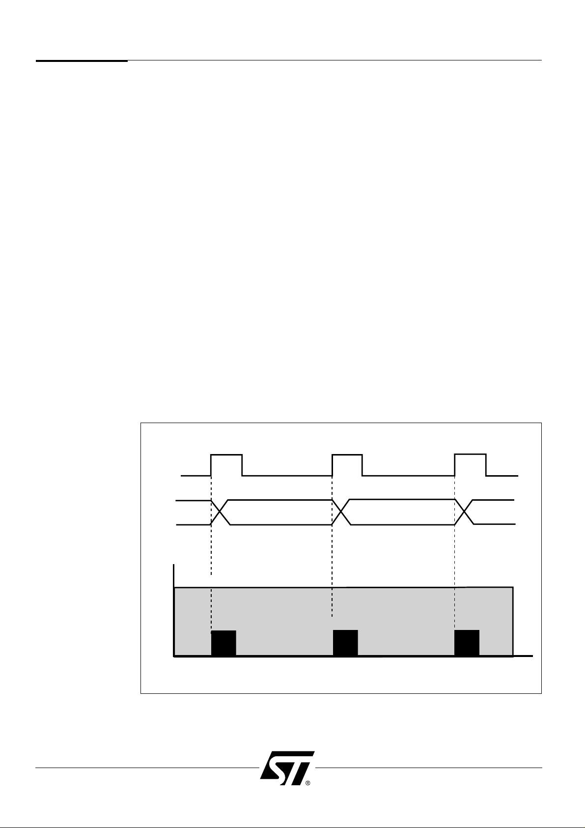
7.1 Integrated Power ManagementTMOperation
Upon each address or logic input change to the ZPSD, the device powers up from low
power standby for a short time. Then the ZPSD consumes only the necessary power to
deliver new logic or memory data to its outputs as a response to the input change. After the
new outputs are stable, the ZPSD latches them and automatically reverts back to standby
mode. The ICCcurrent flowing during standby mode and during DC operation is identical
and is only a few microamperes.
The ZPSD automatically reduces its DC current drain to these low levels and does not
require controlling by the CSI (Chip Select Input). Disabling the CSI pin unconditionally
forces the ZPSD to standby mode independent of other input transitions. The only
significant power consumption in the ZPSD occurs during AC operation. The ZPSD
contains the first architecture to apply Zero-power techniques to memory and logic blocks.
Figure 2 compares ZPSD zero power operation to the operation of a discrete solution.
A standard microcontroller (MCU) bus cycle usually starts with an ALE (or AS) pulse and
the generation of an address. The ZPSD detects the address transition and powers up for a
short time. The ZPSD then latches the outputs of the PAD and EPROM to the new values.
After finishing these operations, the ZPSD shuts off its internal power, entering standby
mode. The time taken for the entire cycle is less than the ZPSD’s “access time.”
The ZPSD will stay in standby mode while its inputs are not changing between bus
cycles. In an alternate system implementation using discrete EPROM, and other discrete
components, the system will consume operating power during the entire bus cycle.
This is because the chip select inputs on the memory devices are usually active throughout
the entire cycle. The AC power consumption of the ZPSD may be calculated using the
composite frequency of the MCU address and control signals, as well as any other logic
inputs to the ZPSD.
ALE
DISCRETE EPROM & LOGIC
ADDRESS
EPROM
ACCESS
EPROM
ACCESS
EPROM
ACCESS
I
CC
ZPSD ZPSD
ZPSD
TIME
Figure 2. ZPSD Power Operation vs. Discrete Implementation
PSD211R Family
7
Name Type Description
This pin is for 8031 or compatible MCUs that use PSEN to
separate program space from data space. In this case, PSEN is
used for reads from the EPROM.
PSEN I Notes:
1) If your MCU does not output a PSEN signal, pull up this pin to
VCC.
2) In programming mode, this pin is pulsed between VPPand 0 V.
The following control signals can be connected to this port, based on
WR/V
PP
your MCU (and the way you configure the PSD in PSDsoft):
or I 1. WR—active-low write pulse.
R/W/V
PP
2. R/W—active-high read/active-low write input.
Note: in programming mode, this pin must be tied to VPP.
The following control signals can be connected to this port, based on
RD/E I
your MCU (and the way you configure the PSD in PSDsoft):
1. RD—active-low read input.
2. E—E clock input.
The following control signals can be connected to this port:
1. CSI-Active-low chip select input. If your MCU supports a chip
select output, and you want the PSD to save power when not
A19/CSI I selected, use this pin as a chip select input.
2. If you don’t wish to use the CSI feature, you may use this pin as
an additional input (logic or address) to the PAD. A19 can be
latched with ALE/AS, or be a transparent logic input.
PSD211R/ZPSD211R:
This pin is user-programmable and can be configured to reset on a
high- or low-level input. Reset must be applied for at least 100 ns.
Reset I
ZPSD211RV:
This pin is not configurable, and the chip will only reset on an
active-low level input. Reset must be applied for at least 500 ns,
and no operations may take place for an additional 500 ns minimum.
(See Figure 8.)
ALE/AS I
Connect ALE or AS to this pin. The polarity of this pin is configurable.
The trailing edge of ALE/AS latches all multiplexed address inputs.
PA0
PA1
PA2
These pins make up Port A. These port pins are configurable, and
PA3
I/O
can have the following functions: (see Figure 5)
PA4
1. MCU I/O—in this mode, the direction of the pin is defined by its
PA5
direction bit, which resides in the direction register.
PA6
2. Latched address output.
PA7
PB0
These pins make up Port B. These port pins are configurable, and
PB1
can have the following functions: (see Figure 6)
PB2
1. MCU I/O—in this mode, the direction of the pin is defined by its
PB3
I/O direction bit, which resides in the direction register.
PB4
2. Chip select output—each of PB0-3 has four product terms
PB5
available per pin, while PB4-7 have 2 product terms each.
PB6
See Figure 4.
PB7
Legend:
The Type column abbreviations are: I = input only; I/O = input/output; P = power.
Table 2.
PSD211R Pin
Descriptions
Table 1.
PSD211R Pin
Descriptions
(cont.)
PSD211R Family
8
Name Type Description
These pins make up Port C. These port pins are configurable, and
can have the following functions (see Figure 7):
1. PAD input—when configured as an input, a bit individually
PC0 becomes an address or a logic input, depending on your PSDsoft
PC1 I/O design file. When declared as an address, the bits are latched
PC2 with ALE/AS.
2. PAD output—when configured as an output (i.e. there is an
equation written for it in your PSDsoft design file), there is one
product term available to it.
AD0
AD1
AD2
These pins are the multiplexed, low-order address/data byte
AD3
I/O
(AD0-AD7). As inputs, address information is latched by the ALE/AS
AD4
signal and used internally by the PSD. The pins also serve as MCU
AD5
data bus inputs or outputs, depending on the MCU control signals
AD6
(RD, WR, etc.).
AD7
A8
A9
A10
A11
I/O These pins are the high-order address inputs (A8-A15).
A12
A13
A14
A15
GND P Ground Pin
V
CC
P Supply voltage input.
Legend:
The Type column abbreviations are: I = input only; I/O = input/output; P = power.
Port Configurations
A I/O or low-order (latched) address lines
B I/O and/or CS0–CS7
C A16-A18 or CS8-CS10
PSD211R Family
9
The PSD211R operates in 8-bit address/data mode, enabling it to interface directly to a
variety of 8-bit multiplexed microcontrollers. It works as follows: the address/data bus
(AD0-AD7) is bi-directional and permits the latching of the address when the ALE/AS signal
is active. On the same pins, the data is read from or written to the device, depending on the
state of the control signals (WR, RD, etc.). You should connect your MCU according to the
following figure. Ports A through C can be configured according to Table 3, below.
Your
8-bit
MCU
PSD211R
PA
PB
PC
AD0-AD7
I/O or A0-A7A8-A15
ALE/AS
PSEN
R/W or WR
RD/E
A19/CSI
RESET
A16-A18
1
I/O or CS0-CS7
CS8-CS10
OR
Figure 3. Connecting a PSD211R to an 8-Bit Multiplexed-Bus MCU
8.0
Operating Mode
Table 3. Bus and Port Configuration Options
9.0
Programmable
Address
Decoder (PAD)
NOTE: 1. Connect A16-A18 to Port C if your MCU outputs more than 16 bits of address.
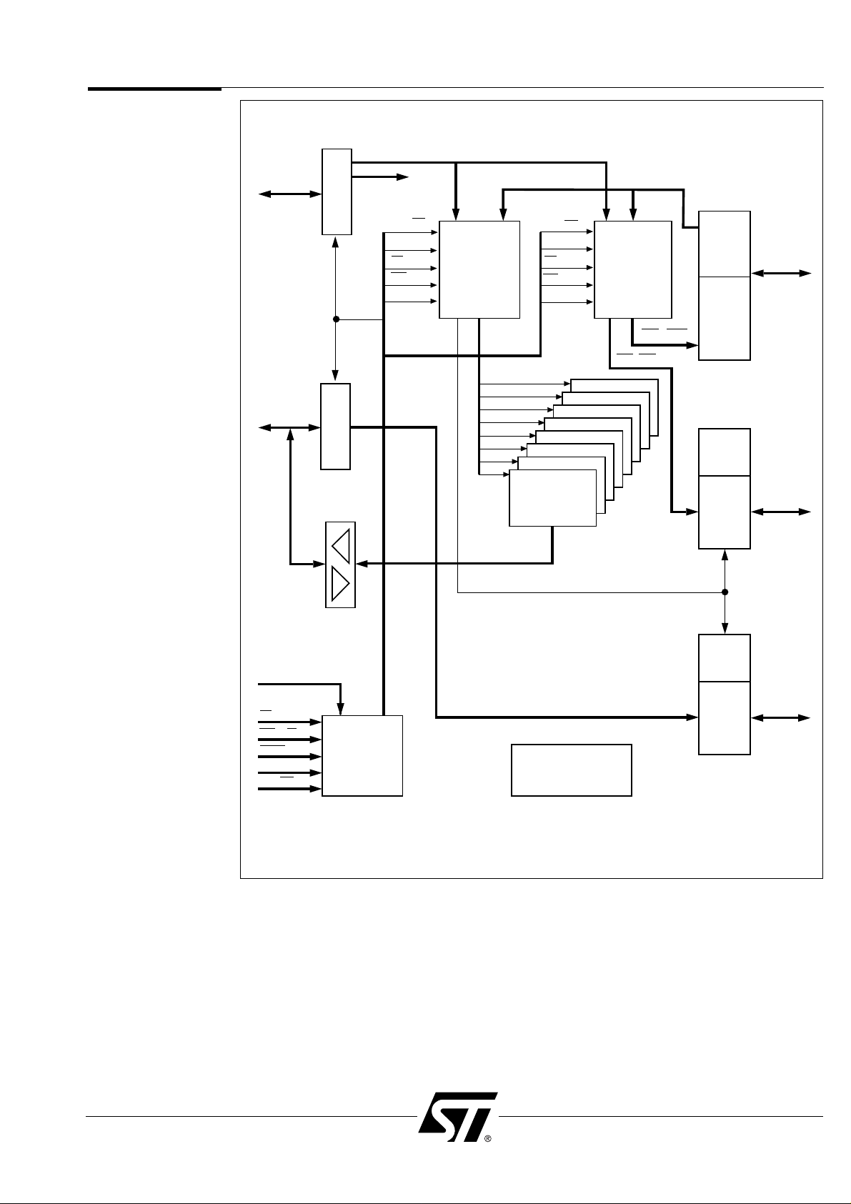
The PSD211R contains two programmable arrays, referred to as PAD A and PAD B
(Figure 4). PAD A is used to generate chip select signals derived from the input address to
the internal EPROM blocks and I/O ports.
PAD B outputs to Ports B and C for off-chip usage. PAD B can also be used to extend the
decoding to select external devices or as a random logic replacement.
PAD A and PAD B receive the same inputs. The PAD logic is configured by PSDsoft based
on the designer’s input. The PAD’s non-volatile configuration is stored in a re-programmable
CMOS EPROM. Windowed packages are available for erasure by the user. See Table 4 for
a list of PAD A and PAD B functions.
NOTES: 1. CSI is a power-down signal. When high, the PAD is in stand-by mode and all its outputs
become non-active. See Tables 7A and 7B.
2. RESET deselects all PAD output signals. See Tables 8A and 8B.
3. A18, A17, and A16 are internally multiplexed with CS10, CS9, and CS8, respectively.
Either A18 or CS10, A17 or CS9, and A16 or CS8 can be routed to the external pins of
Port C. Port C can be configured as either input or output.
ALE or AS
WR or R/W
A19
A18
A17
A16
A15
A14
A13
A12
A11
ES0
ES1
ES2
ES3
ES4
ES5
ES6
ES7
CSIOPORT
CS0/PB0
CS1/PB1
CS2/PB2
CS3/PB3
CS4/PB4
CS5/PB5
CS6/PB6
CS7/PB7
CS8/PC0
CS9/PC1
CS10/PC2
RD/E
8 EPROM BLOCK
SELECT LINES
CSI
RESET
I/O BASE ADDRESS
PAD
B
PAD
A
PSD211R Family
10
Figure 4. PAD Description
Programmable
Address
Decoder (PAD)
PSD211R Family
11
Function
PAD A and PAD B Inputs
In CSI mode (when high), PAD deselects all of its outputs and enters a
A19/CSI power-down mode (see Tables 7A and 7B). In A19 mode, it is another
input to the PAD.
A16–A18 These are general purpose inputs from Port C. See Figure 4, Note 3.
A11–A15 These are address inputs.
RD/E This is the read pulse or enable strobe input.
WR or R/W This is the write pulse or R/W select signal.
ALE/AS This is the ALE or AS input to the chip.
RESET
This deselects all outputs from the PAD; it can not be used in product
term equations.See Tables 8A and 8B.
PAD A Outputs
These are internal chip-selects to the 8 EPROM banks. Each bank can
ES0–ES7 be located on any boundary that is a function of one product term of the
PAD address inputs.
This internal chip-select selects the I/O ports. It can be placed on any
CSIOPORT boundary that is a function of one product term of the PAD inputs. See
Table 5.
PAD B Outputs
CS0–CS3
These chip-select outputs can be routed through Port B. Each of them is
a function of up to four product terms of the PAD inputs.
CS4–CS7
These chip-select outputs can be routed through Port B. Each of them is
a function of up to two product terms of the PAD inputs.
CS8–CS10
These chip-select outputs can be routed through Port C. See Figure 4,
Note 3. Each of them is a function of one product term of the PAD inputs.
Table 4. PSD211R PAD A and PAD B Functions
Programmable
Address
Decoder (PAD)
(cont.)
PSD211R Family
12
10.0
I/O Port
Functions
The PSD211R has three I/O ports (Ports A, B, and C) that are configurable at the bit level.
This permits great flexibility and a high degree of customization for specific applications.
The next section describes the control registers for the ports. Following that are sections
that describe each port. Figures 5 through 7 show the structure of Ports A through C,
respectively.
Note: any unused inputs should be connected directly to ground or pulled up to VCC(using
a 10KΩ to 100KΩ resistor).
10.1 CSIOPORT Registers
Control of the ports is primarily handled through the CSIOPORT registers. There are 24
bytes in the address space, starting at the base address labeled CSIOPORT. Since the
PSD211R uses internal address lines A15-A11 for decoding, the CSIOPORT space
will occupy 2 Kbytes of memory, on a 2 Kbyte boundary. This resolution can be improved
to reduce wasted address space by connecting lower order address lines (A10 and below)
to Port C. Using this method, resolution down to 256 Kbytes may be achieved. The
CSIOPORT space must be defined in your PSDsoft design file. The following tables list
the registers located in the CSIOPORT space.
Table 5. CSIOPORT Registers for 8-Bit Data Busses
NOTE: 1. ZPSD only.
Offset (in hex) Type of
from CSIOPORT Access
Register Name Base Address Allowed
Port A Pin Register +2 Read
Port A Direction Register +4 Read/Write
Port A Data Register +6 Read/Write
Port B Pin Register +3 Read
Port B Direction Register +5 Read/Write
Port B Data Register +7 Read/Write
Power Management Register (Note 1) +10 Read/Write
10.2 Port A (PA0-PA7)
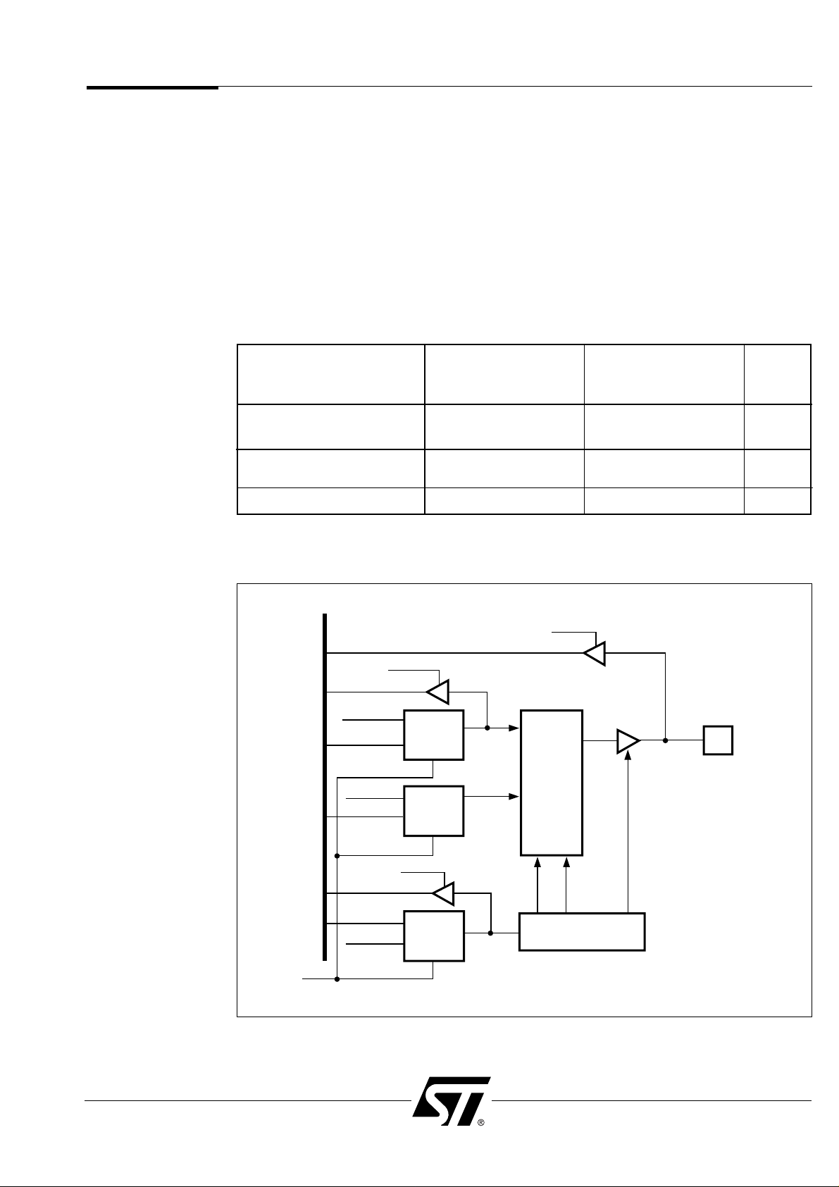
MCU I/O Mode
The default configuration of Port A is MCU I/O. In this mode, every pin can be set
(at run-time) as an input or output by writing to the respective pin’s direction flip-flop
(DIR FF, Figure 5). As an output, the pin level can be controlled by writing to the respective
pin’s data flip-flop (DFF, Figure 5A). The Pin Register can be read to determine logic level
of the pin. The contents of the pin register indicate the true state of the PSD driving the pin
through the DFF or an external source driving the pin.
13
PSD211R
10.0
I/O Port
Functions
(Cont.)
10.2 Port A (PA0-PA7)
(Cont.)
Latched Address Output Mode
Alternatively, any bit(s) of Port A can be configured to output a low-order demultiplexed
address bus bit. The address is provided by the internal PSD address latch, which latches
the address on the trailing edge of ALE/AS. Port A then outputs the desired demultiplexed
address bits. This feature can eliminate the need for an external latch (for example:
74LS373) if you have devices that require low-order latched address bits. Although any pin
of Port A may output an address signal, the pin is position-dependent. In other words, pin
PA0 of Port A may only pass A0, PA1 only A1, and so on.
The control registers of Port A are located in CSIOPORT space; see Table 5. Each pin of
Port A can be individually configured. The following table summarizes what the control
registers (in CSIOPORT space) for Port A do:
NOTE: 1. Default value is the value after reset.
Default
Value
Register Name 0 Value 1 Value
(Note 1)
Port A Pin Register
Sampled logic level Sampled logic level
X
at pin = ‘0’ at pin = ‘1’
Port A Direction Register
Pin is configured Pin is configured
0
as input as output
Port A Data Register Data in DFF = ‘0’ Data in DFF = ‘1’ 0
Figure 5. Port A Pin Structure
READ PIN
PORT A PIN
ENABLE
LATCHED
ADDR
OUT
MCU
I/O
OUT
READ DATA
WRITE DATA
ALE
READ DIR
WRITE DIR
RESET
CK
D
R
G
D
R
D
CK
R
I
N
T
E
R
N
A
L
A
D
D
R
/
D
A
T
A
B
U
S
A
D
0
/
A
D
7
DFF
LATCH
DIR
FF
CONTROL
MUX
 Loading...