

Datasheet NE556N, NE556, NE556D, SA556, SA556D Datasheet (SGS Thomson Microelectronics)
...
NE556
GENERAL PURPOSE DUAL BIPOLAR TIMERS
.LOW TURN OFF TIME
.MAXIMUM OPERATING FREQUENCY
GREATERTHAN500kHz
.TIMINGFROMMICROSECONDSTO HOURS
.OPERATES IN BOTH ASTABLE AND
MONOSTABLEMODES
.HIGHOUTPUT CURRENT CAN SOURCE OR
SINK200mA
.ADJUSTABLE DUTYCYCLE
.TTL COMPATIBLE
.TEMPERATURESTABILITYOF 0.005%
DESCRIP T IO N
TheNE556 dual monolithictiming circuit is a highly
stablecontrollercapableofproducingaccuratetime
delaysor oscillation.In the time delaymode of operation,the time ispreciselycontrolledby oneexternalresistorand capacitor.For a stableoperationas
anoscillator,thefreerunningfrequencyandtheduty
cycleare both accuratelycontrolledwith two externalresistorsand one capacitor.Thecircuit maybe
triggered and reset on falling waveforms, and the
outputstructurecansourceor sink up to 200mA.
PER
o
C
N
DIP14
(PlasticPackage)
ORDER CODES
Part
Number
NE556 0
SA556 –40
SE556 –55
Temperature
SA556 - SE556
D
SO14
(PlasticMicropackage)
Pakcage
Range
o
C, 70oC ••
o
C, 105oC ••
o
C, 125oC ••
ND
PI N CO NNECT IONS (top v iew)
Discharge
Threshold
Control Voltage
Re s et
Output
Trigger
GND
July 1998
1
2
3
4
5
6
7
14
V
Discha rge
13
Threshold
12
Control Voltage
11
Re s et
10
Output
9
Trigger
8
CC
1/9
NE 556/SA556/ SE556
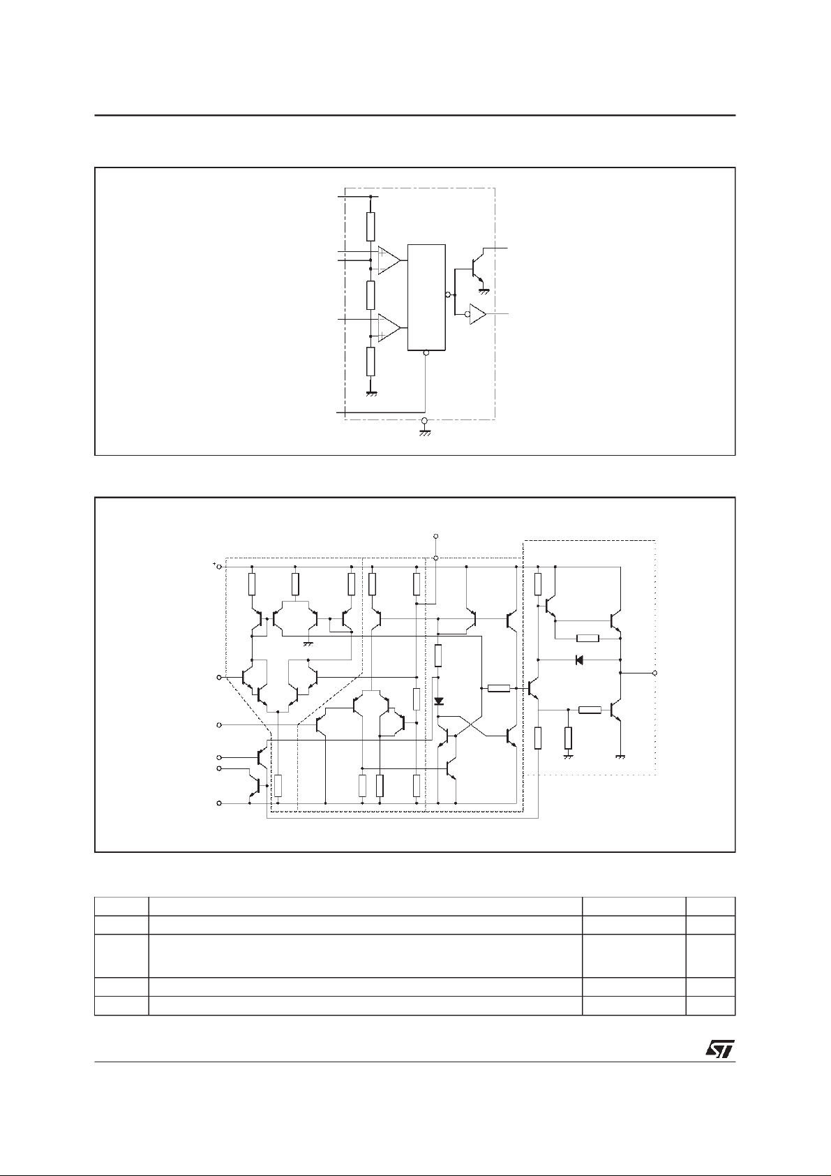
BLOCK DIAGRAM
THRES HOLD
CONTROL VOLTAGE
TRIGGER
+
V
CC
Ω
5k
COMP
Ω
5k
COMP
Ω
5k
R
FLIP-FLOP
S
INHIBIT/
RESET
Q
DISCHARGE
OUT
1/2 NE556
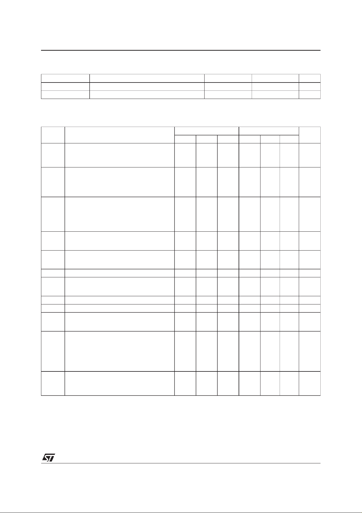
SCHE MATIC DIAGRAM
THRESHOLD
COMPARATOR
V
CC
Q5 Q6 Q7 Q8 Q9
THRESHOLD
TRIGGER
RESET
DISCHARGE
GND
Q1
2
4
7
Q14
1
4.7k
R1
Q2
Q15
RESET
R2
R3
830
Ω
Ω
Q3
R5
10kΩ
4.7k
Q4
Q10
100kΩR7100kΩ
Ω
R6
Q11 Q12
R4
1k
Ω
Q13
S
CONTROL
VOLTAGE
R8
5k
Ω
R9
5kΩ
Q16 Q18
R10
5kΩ
OUTPUT
5
R12
6.8k
Ω
Q20
Q23
100
R16
Q21
Q22
Ρ13
3.9kΩ
D1
R14
220Ω
R15
4.7kΩ
Ω
3
Q24
R11
5kΩ
Q19
R17
4.7k
Ω
D2
Q17
TRIGGER COMPARATOR FLIP FLOP
ABSOLUTE MAXIMUM RATINGS
Symbol Parameter Value Unit
Supply Voltage 18 V
V
cc
T
T
2/9
Operating Free Air Temperature Range for NE556
oper
for SA556
for SE556
Junction Temperature 150 °C
T
j
Storage Temperature Range – 65 to 150 °C
stg
0to70
–40 to 105
–55 to 125
°C
NE 556/SA556/ SE556
OPERATINGCONDITIONS
Symbol Parameter SE556 NE556 - SA556 Unit
V
CC
V
th,Vtrig,Vcl,Vreset
ELECTRICAL CHARACTERISTICS
= +25oC, VCC= +5V to +15V (unless otherwise specified)
T
amb
Symbol Parameter
I
V
V
V
I
V
V
Notes : 1. Supply current when output is high is typically 1mA less.
Supply Current (RL∞) (- note 1) - (2 timers)
CC
Low State V
High State V
Timing Error (monostable)
(R
A=
Initial Accuracy - (note 2)
Drift with Temperature
Drift with Supply Voltage
Timing Error (astable)
(R
A,RB
V
CC
Initial Accuracy - (note 2)
Drift with Temperature
Drift with Supply Voltage
Control Voltage level
CL
Threshold Voltage
V
th
Threshold Current - (note 3) 0.1 0.25 0.1 0.25 µA
I
th
Trigger Voltage
trig
Trigger Current (V
I
trig
Reset Voltage - (note 4) 0.4 0.7 1 0.4 0.7 1 V
reset
Reset Current
reset
Low Level Output Voltage
OL
V
CC
V
CC
High Level Output Voltage
OH
V
CC
V
CC
2. Tested at V
3. This willdetermine the maximum value of R
the max total R = 3.5MΩ.
4. Specified with trigger input high.
Supply Voltage 4.5 to 18 4.5 to 18 V
Maximum Input Voltage V
CC
V
CC
SE556 NE556 - SA556
Min. Typ. Max. Min. Typ. Max.
V
CC
CC
CC
= +5V
= +15V
=5V
20
6
4
10
24
6
20
4
2k to 100kΩ, C = 0.1µF)
0.5
30
0.05
2
100
0.2
1
50
0.130.5
=1kΩto 100kΩ, C = 0.1µF,
= +15V)
= +15V, I
= +5V, I
= +15V, I
= +5V, I
= +5V and VCC= +15V.
CC
1.5
90
0.15
= +15V
V
CC
= +5V
V
CC
= +15V
V
CC
= +5V
V
CC
= +15V
V
CC
= +5V
V
CC
= 0V) 0.5 0.9 0.5 2.0 µA
trig
= +0.4V
V
reset
=0V
V
reset
= 10mA
O(sink)
= 50mA
I
O(sink)
= 100mA
I
O(sink)
= 200mA
I
O(sink)
= 8mA
O(sink)
= 5mA
I
O(sink)
O(source)
I
O(source)
O(source)
= 200mA
= 100mA
= 100mA
A+RB
9.6
2.9
9.4
2.7
4.8
1.4551.67
13
3
for +15Voperation the max total is R = 20MΩ and for 5V operation
10
3.33
10
3.33
0.1
0.4
0.1
0.4
2
2.5
0.1
0.05
12.5
13.3
3.3
10.4
3.8
10.6
4
5.2
1.9
0.4
1
0.15
0.5
2.2
0.25
0.2
2.6103.33
8.8
2.4103.33
4.5
1.151.67
12.75
2.75
2.25
150
0.3
9
0.1
0.4
0.1
0.4
2
2.5
0.3
0.25
12.5
13.3
3.3
V
Unit
mA
12
30
%
ppm/°C
%/V
%
ppm/°C
%/V
V
11
4
V
11.2
4.2
V
5.6
2.2
mA
0.4
1.5
V
0.25
0.75
2.5
0.4
0.35
V
3/9

NE 556/SA556/ SE556
ELECTRICAL CHARACTERISTICS (continued)
Symbol Parameter
I
dis(off)
V
dis(sat)
Notes : 5. No protection against excessive Pin 7 current isnecessary, providing the package dissipation rating will notbe exceeded.
Discharge Pin Leakage Current
(output high) (V
dis
= 10V)
Discharge pin Saturation Voltage
(output low) - (note 5)
= +15V, I
V
CC
= +5V, I
V
CC
Output Rise Time
t
r
t
Output Fall Time
f
t
Turn off Time - (note 6) (V
off
6. Timemesaured from a positive going input pulse from 0 to 0.8x V
output trigger istied to treshold.
dis
= 4.5mA
dis
= 15mA
reset=VCC
) 0.5 0.5 µs
Min. Typ. Max. Min. Typ. Max.
SE556 NE556 - SA556
20 100 20 100 nA
180
80
100
100
CC
480
200
200
200
into the threshold to the drop from high to low of the
180
80
100
100
480
200
300
300
Unit
mV
ns
Figure1 : MinimumPulseWidth Requiredfor
Figure 2 : SupplyCurrent versusSupplyVoltage
Trigering
Figure 3 : Delay Time versusTemperature Figure4 : LowOutputVoltageversus Output
SinkCurrent
4/9

NE 556/SA556/ SE556
Figure 5 : Low OutputVoltage versusOutput
SinkCurrent
Figure7 : HighOutput VoltageDrop versus
Output
Figure6 : LowOutputVoltageversusOutput
SinkCurrent
Figure8 : Delay Time versusSupply Voltage
Figure9 : PropagationDelay versusVoltage
Level of Trigger Value
5/9

NE 556/SA556/ SE556
TYP ICAL APPLIC ATI O N
50 % DUTY CYCLE OSCIL LATOR
V
CC
6
Output
5
t1= 0.693 RA.C
t
= [(RARB)⁄ (R
2
1
f =
t
1+t2
RB<
(8)
(9)
4
(10)
+ R
A
B
1
R
A
2
1/2
NE556
SE556
7
)] CLn
ti
14
(13)
1
(12)
2
(11)
3
R
− 2R
B
− R
A
A
B
2R
t2
R
s
22k
0.01nF
PULSE WIDTH MODULATOR
V
CC
R
A
Ω
51k
Trigger
Ω
Output
C
4
(10)
6
(8)
14
(13)
1
1/2
NE556
SE556
(9)
5
7
MODULATION
(12)
(11)
INPUT
2
3
R
A
C
6/9
t1

NE 556/SA556/ SE556
TONE BURS T GENE RATOR
For a tone burst generatorthe first timer is usedas a monostable and determinesthe tonedurationwhen
triggeredby a positive pulse at pin 6. Thesecondtimeris enabledby thehigh output os the monostable.It
is connectedas anastableanddeterminesthefrequency of thetone.
Trigge r
6
Discharge
1
2
Thre shold
Res et
1/2
NE556
SE556
Ground
T=1.1R .C1
R
Trigge r
C1
t
MONOSTABLE OP E RATION
V
CC
R
L
4
Trigger
(10)
(8)
6
1/2
NE556
SE556
Vcc414
t
14
(13)
R
A
R
B
C2
Ground
+15V
0.01
Control
µ
F
5
Output
3
10
Res et
Output
14
Discharge
13
1/2
NE556
SE556
9
Ground
1.44
f=
R+2R)C
A
12
Thre shold
8
Trigge r
Control
11
µ
0.01
F
B
ASTABLE O PE RAT I ON
V
CC
R
R
A
1
L
4
(10)
14
(13)
1
1/2
Output
(9)
5
NE556
SE556
R
A
R
B
Output
t2
(12)
2
(8)
6
1.44
f=
R+2R)C
A
C
B
(12)
(9)5
(11)
7
R
L
2
3
10nF
C
R
L
(11)
7
3
0.01nF
Operating frequency
T=1.1R .C
A
=0.693(RA+RB) COutput High
t
1
t
=0.693RBC OutputLow
2
t1
7/9

NE 556/SA556/ SE556
PACKAG E MECHANICAL DATA
14 P I NS - PLASTIC DIP
Dimensions
a1 0.51 0.020
B 1.39 1.65 0.055 0.065
b 0.5 0.020
b1 0.25 0.010
D 20 0.787
E 8.5 0.335
e 2.54 0.100
e3 15.24 0.600
F 7.1 0.280
i 5.1 0.201
L 3.3 0.130
Z 1.27 2.54 0.050 0.100
Min. Typ. Max. Min. Typ. Max.
Millimeters Inches
8/9

PACKAG E MECHANICAL DATA
14 PINS - PLASTIC MICROPACKAGE (SO)
NE 556/SA556/ SE556
Dimensions
Min. Typ. Max. Min. Typ. Max.
Millimeters Inches
A 1.75 0.069
a1 0.1 0.2 0.004 0.008
a2 1.6 0.063
b 0.35 0.46 0.014 0.018
b1 0.19 0.25 0.007 0.010
C 0.5 0.020
c1 45
o
(typ.)
D 8.55 8.75 0.336 0.334
E 5.8 6.2 0.228 0.244
e 1.27 0.050
e3 7.62 0.300
F 3.8 4.0 0.150 0.157
G 4.6 5.3 0.181 0.208
L 0.5 1.27 0.020 0.050
M 0.68 0.027
S8
Information furnished is believed to be accurate and reliable. However, STMicroelectronics assumes no responsibility for the
consequences of use of such information nor for any infringement of patents or other rights of third parties which may result
from its use. No license is granted by implication or otherwise under any patent or patent rights of STMicroelectronics. Specifications mentioned in this publication are subject to change without notice. This publication supersedes and replaces all information previously supplied. STMicroelectronics products are not authorized for use as critical components in life support
devices or systems without express written approval of STMicroelectronics.
The ST logo is a trademark of STMicroelectronics
o
(max.)
1998 STMicroelectronics – Printed in Italy – AllRights Reserved
STMicroelectronics GROUP OF COMPANIES
Australia - Brazil - Canada - China - France - Germany - Italy - Japan - Korea - Malaysia - Malta- Mexico - Morocco
The Netherlands - Singapore - Spain - Sweden - Switzerland - Taiwan - Thailand - United Kingdom- U.S.A.
9/9
 Loading...