

Page 1

Philips Semiconductors Product specification
NE/SA568A150MHz phase-locked loop
1
1996 Feb 1 853-1558 16328
DESCRIPTION
The NE568A is a monolithic phase-locked loop (PLL) which
operates from 1Hz to frequencies in excess of 150MHz and features
an extended supply voltage range and a lower temperature
coefficient of the V
CO
center frequency in comparison with its
predecessor, the NE 568. The NE568A is function and
pin-compatible with the NE568, requiring only minor changes in
peripheral circuitry (see Figure 3). Temperature compensation
network is different, no resistor on Pin 12, needs to be grounded and
Pin 13 has a 3.9kΩ resistor to ground. Timing cap, C
2
, is different
and for 70MHz operation with temperature compensation network
should be 16pF, not 34pF as was used in the NE568. The NE568A
has the following improvements: ESD protected; extended V
CC
range from 4.5V to 5.5V; operating temperature range -55 to 125°C
(see Signetics Military 568A data sheet); less layout sensitivity; and
lower T
C
of VCO (center frequency). The integrated circuit consists
of a limiting amplifier, a current-controlled oscillator (ICO), a phase
detector, a level shift circuit, V/I and I/V converters, an output buf fer,
and bias circuitry with temperature and frequency compensating
characteristics. The design of the NE568A is particularly well-suited
for demodulation of FM signals with extremely large deviation in
systems which require a highly linear output. In satellite receiver
applications with a 70MHz IF, the NE568A will demodulate ±20%
deviations with less than 1.0% typical non-linearity. In addition to
high linearity, the circuit has a loop filter which can be configured
with series or shunt elements to optimize loop dynamic
performance. The NE568A is available in 20-pin dual in-line and
20-pin SO (surface mounted) plastic packages.
FEATURES
•Operation to 150MHz
•High linearity buffered output
PIN CONFIGURATION
V
CC2
GND1
D, N Packages
LF1
V
CC1
REFBYP
PNPBYP
INPBYP
LF3
LF2
LF4
FREQ ADJ
1
2
3
4
5
6
7
8
9
10
11
12
13
14
20
19
18
17
16
15
OUT
FILT
V
OUT
TC
ADJ2
V
IN
TC
ADJ1
GND
2
GND
1
TCAP1
TCAP2
TOP VIEW
SR01037
Figure 1. Pin Configuration
•Series or shunt loop filter component capability
•External loop gain control
•Temperature compensated
•ESD protected
1
APPLICATIONS
•Satellite receivers
•Fiber optic video links
•VHF FSK demodulators
•Clock Recovery
ORDERING INFORMATION
DESCRIPTION TEMPERATURE RANGE ORDER CODE DWG #
20-Pin Plastic Small Outline Large (SOL) Package 0 to +70°C NE568AD SOT163-1
20-Pin Plastic Dual In-Line Package (DIP) 0 to +70°C NE568AN SOT146-1
20-Pin Plastic Small Outline Large (SOL) Package -40 to +85°C SA568AD SOT163-1
20-Pin Plastic Dual In-Line Package (DIP) -40 to +85°C SA568AN SOT146-1
BLOCK DIAGRAM
PHASE
DETECTOR
1 2 3 4 5 6 7 8 9 10
111213141516
17181920
LEVEL SHIFT
V/I
CONVERTER
AMP
I/V
CONVERTER
OUT
BUF
LEVEL SHIFT
TCADJ BIAS
ICO
V
CC2
GND1
LF1
V
CC1
REFBYP PNPBYP INPBYP
LF3LF2 LF4 FREQ ADJ
OUT
FILTVOUT
TC
ADJ2
V
IN
TC
ADJ1
GND
2
GND
1
TCAP1 TCAP2
NOTE:
Pins 4 and 5 can tolerate
1000V only, and all other
pins, greater than 2000V
for ESD (human body
model).
SR01038
Figure 2. Block Diagram
Page 2

Philips Semiconductors Product specification
NE/SA568A150MHz phase-locked loop
1996 Feb 1
2
ABSOLUTE MAXIMUM RATINGS
SYMBOL PARAMETER RATING UNITS
V
CC
Supply voltage 6 V
T
J
Junction temperature +150 °C
T
STG
Storage temperature range -65 to +150 °C
P
DMAX
Maximum power dissipation 400 mW
θ
JA
Thermal resistance 80 °C/W
ELECTRICAL CHARACTERISTICS
The elctrical characteristics listed below are actual tests (unless
otherwise stated) performed on each device with an automatic IC
tester prior to shipment. Performance of the device in automated
test set-up is not necessarily optimum. The NE568A is
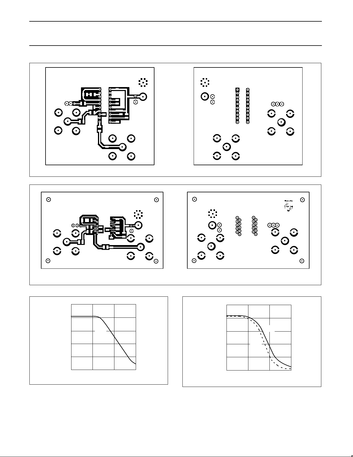
layout-sensitive. Evaluation of performance for correlation to the
data sheet should be done with the circuit and layout of Figures 3, 4,
and 5 with the evaluation unit soldered in place. (Do not use a
socket!)
DC ELECTRICAL CHARACTERISTICS
VCC = 5V; TA = 25°C; fO = 70MHz, Test Circuit Figure 3, fIN = -20dBm, R4 = 3.9kΩ, unless otherwise specified.
LIMITS
SYMBOL
PARAMETER
TEST CONDITIONS
NE/SA568A
UNITS
MIN TYP MAX
V
CC
Supply voltage 4.5 5 5.5 V
I
CC
Supply current 54 70 mA
AC ELECTRICAL CHARACTERISTICS
LIMITS
SYMBOL
PARAMETER
TEST CONDITIONS
NE/SA568A
UNITS
MIN TYP MAX
f
OSC
Maximum oscillator operating frequency
3
150 MHz
Input signal level
50
–20
1
2000
+10
mV
P-P
dBm
BW Demodulated bandwidth fO/7 MHz
Non-linearity
5
Dev = ±20%, Input = -20dBm 1.0 4.0 %
Lock range
2
Input = -20dBm ±25 ±35 % of f
O
Capture range
2
Input = -20dBm ±20 ±30 % of f
O
TC of f
O
Figure 3 100 ppm/°C
R
IN
Input resistance
4
1 kΩ
Output impedance 6 Ω
Demodulated V
OUT
Dev = ±20% of fO measured at
Pin 14
0.40 0.52 V
P-P
AM rejection
VIN = -20dBm (30% AM)
referred to ±20% deviation
50 dB
f
O
Distribution
6
Centered at 70MHz, R2 =
1.2kΩ, C
2
= 16pF, R4 = 3.9kΩ
(C
2
+ C
STRAY
= 20pF)
-15 0 +15 %
f
O
Drift with supply 4.5V to 5.5V 2 %/V
NOTE:
1. Signal level to assure all published parameters. Device will continue to function at lower levels with varying performance.
2. Limits are set symmetrical to f
O
. Actual characteristics may have asymmetry beyond the specified limits.
3. Not 100% tested, but guaranteed by design.
4. Input impedance depends on package and layout capacitances. See Figures 6 and 5.
5. Linearity is tested with incremental changes in inupt frequency and measurement of the DC output voltage at Pin 14 (V
OUT
). Non-linearity is
then calculated from a straight line over the deviation range specified.
6. Free-running frequency is measured as feedthrough to Pin 14 (V
OUT
) with no input signal applied.
Page 3

Philips Semiconductors Product specification
NE/SA568A150MHz phase-locked loop
1996 Feb 1
3
C1
R
FC1
C2
C8
C3
C4
C5 C6
C7
C13
C12
C11
C9
R
FC2
V
CC
V
OUT
V
IN
C10
R1
R2
R3
R4
R5
V
CC2
GND1
GND2
GND1
TCAP1
TCAP2
V
CC1
REFBYP
PNPBYP
INPBYP
LF1
OUTFILT
LF2
LF3
LF4
FREQADJ
V
OUT
TCADJ2
TCADJ1
V
IN
SR01039
1
2
3
4
5
6
7
8
9
10
20
19
18
17
16
15
14
13
12
11
Figure 3. Test Circuit for AC Parameters
FUNCTIONAL DESCRIPTION
The NE568A is a high-performance phase-locked loop (PLL). The
circuit consists of conventional PLL elements, with special circuitry
for linearized demodulated output, and high-frequency performance.
The process used has NPN transistors with f
T
> 6GHz. The high
gain and bandwidth of these transistors make careful attention to
layout and bypass critical for optimum performance. The
performance of the PLL cannot be evaluated independent of the
layout. The use of the application layout in this data sheet and
surface-mount capacitors are highly recommended as a starting
point.
The input to the PLL is through a limiting amplifier with a gain of 200.
The input of this amplifier is differential (Pins 10 and 11). For
single-ended applications, the input must be coupled through a
DC-blocking capacitor with low impedance at the frequency of
interest. The single-ended input is normally applied to Pin 11 with
Pin 10 AC-bypassed with a low-impedance capacitor. The input
impedance is characteristically slightly above 500Ω. Impedance
match is not necessary, but loading the signal source should be
avoided. When the source is 50 or 75Ω, a DC-blocking capacitor is
usually all that is needed.
Input amplification is low enough to assure reasonable response
time in the case of large signals, but high enough for good AM
rejection. After amplification, the input signal drives one port of a
multiplier-cell phase detector. The other port is driven by the
current-controlled oscillator (ICO). The output of the phase
comparator is a voltage proportional to the phase difference of the
input and ICO signals. The error signal is filtered with a low-pass
filter to provide a DC-correction voltage, and this voltage is
converted to a current which is applied to the ICO, shifting the
frequency in the direction which causes the input and ICO to have a
90° phase relationship.
The oscillator is a current-controlled multivibrator. The current
control affects the charge/discharge rate of the timing capacitor . It is
common for this type of oscillator to be referred to as a
voltage-controlled oscillator (VCO), because the output of the phase
comparator and the loop filter is a voltage. To control the frequency
of an integrated ICO multivibrator, the control signal must be
conditioned by a voltage-to-current converter. In the NE568A,
special circuitry predistorts the control signal to make the change in
frequency a linear function over a large control-current range.
The free-running frequency of the oscillator depends on the value of
the timing capacitor connected between Pins 4 and 5. The value of
the timing capacitor depends on internal resistive components and
current sources. When R
2
= 1.2kΩ and R4 = 0Ω, a very close
approximation of the correct capacitor value is:
O
F
STRAY
(ICO Constant) at 70MHz
The loop filter determines the general characteristics of the loop.
Capacitors C
9
, C10, and resistor R1, control the transient output of
the phase detector. Capacitor C
9
suppresses 70MHz feedthrough
by interaction with 100Ω load resistors internal to the phase
detector.
0.0014
C *
f
where
C * C
2
C
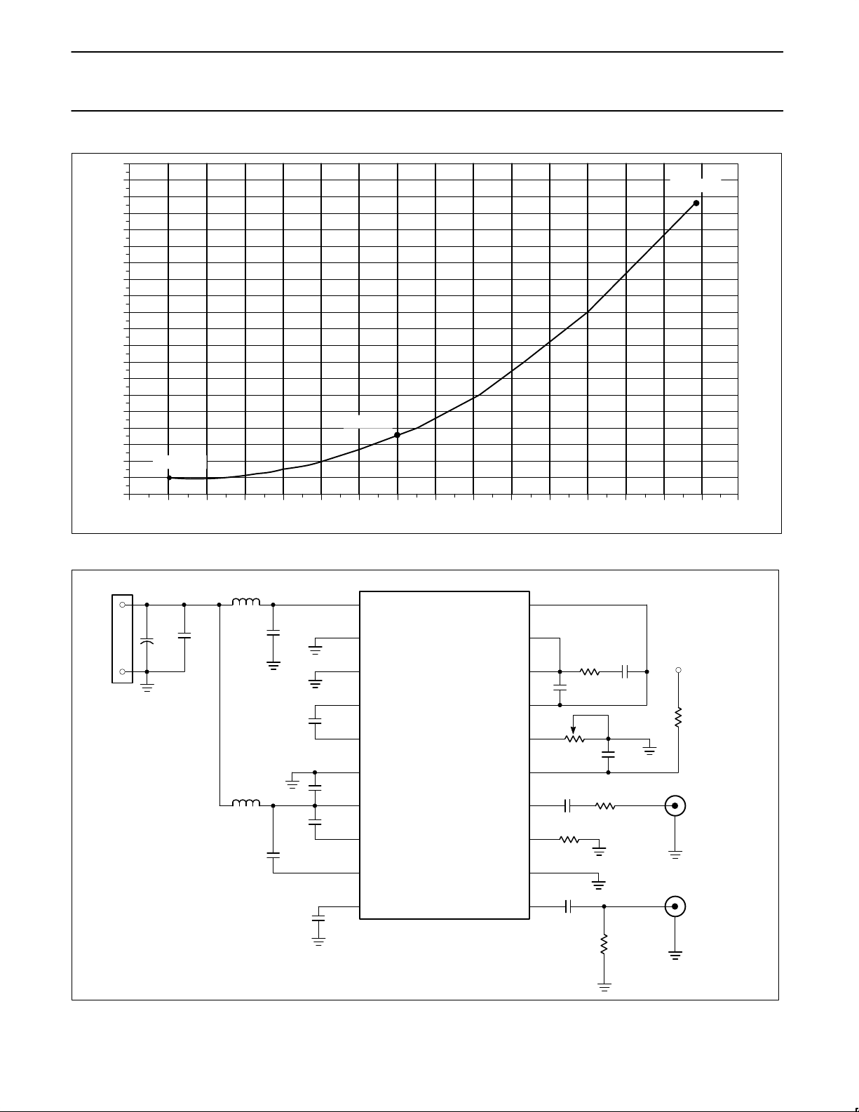
The temperature-compensation resistor, R4, affects the actual value
of capacitance. This equation is normalized to 70MHz. See 10 for
correction factors.
The loop filter determines the dynamic characteristics of the loop. In
most PLLs, the phase detector outputs are internally connected to
the ICO inputs. The NE568A was designed with filter output to input
connections from Pins 20 (φ DET) to 17 (ICO), and Pins 19 (φ DET)
to 18 (ICO) external. This allows the use of both series and shunt
loop-filter elements. The loop constratints are:
K
0.12VRadian (Phase Detector Constant)
O
Radians
KO 4.2 10
9
V
–sec
Page 4
Philips Semiconductors Product specification
NE/SA568A150MHz phase-locked loop
1996 Feb 1
4
C
9
1
2 (50) (fO)
F
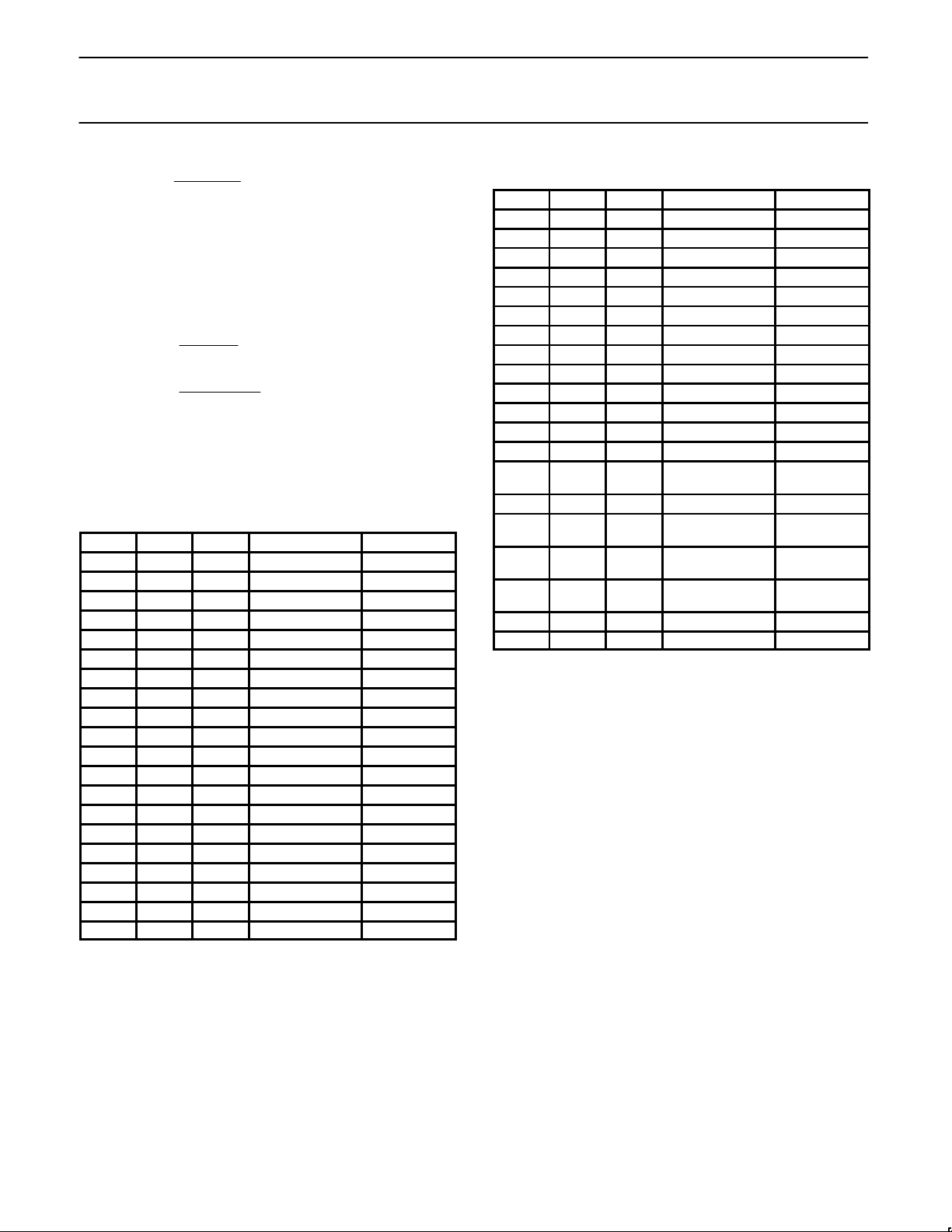
At 70MHz, the calculated value is 45pF. Empirical results with the
test and application board were improved when a 47pF capacitor
was used.
The natural frequency for the loop filter is set by C
10
and R1. If the
center frequency of the loop is 70MHz and the full demodulated
bandwidth is desired, i.e., f
BW
= fO/7 = 10MHz, and a value for R1 is
chosen, the value of C
10
can be calculated.
C
10
1
2 R1f
BW
F
Also,
C
11
1
2350f
BW(Hz)
This capacitance determines the signal bandwidth of the output
buffer amplifier. (For further inofrmation see Philips application note
AN1881 “The NE568A Phase Locked Loop as a Wideband Video
Demodulator”.
Parts List and Layout 40MHz Application NE568AD
C
1
100nF ±10% Ceramic chip 1206
C
2
1
18pF ±2% Ceramic chip 0805
C
2
2
16pF ±2% Ceramic ORChip
C
3
100nF ±10% Ceramic chip 1206
C
4
100nF ±10% Ceramic chip 1206
C
5
6.8µF ±10% Tantalum 35V
C
6
100nF ±10% Ceramic chip 1206
C
7
100nF ±10% Ceramic chip 1206
C
8
100nF ±10% Ceramic chip 1206
C
9
47pF ±2% Ceramic chip 0805 or 1206
C
10
560pF ±2% Ceramic chip 0805 or 1206
C
11
47pF ±2% Ceramic chip 0805 or 1206
C
12
100nF ±10% Ceramic chip 1206
C
13
100nF ±10% Ceramic chip 1206
R
1
27Ω ±10% Chip CR32 1/4W
R
2
1.2kΩ Trim pot
R
3
3
43Ω ±10% Chip CR32 1/4W
R
4
4
3.9kΩ ±10% Chip CR32 1/4W
R
5
3
50Ω ±10% Chip CR32 1/4W
RFC
1
5
10µH ±10% Surface mount
RFC
2
5
10µH ±10% Surface mount
NOTES:
1. 18pF with Pin 12 ground and Pin 13 no connect (open).
2. C
2
+ C
STRAY
= 16pF for temperature-compensated configuration
with R
4
= 3.9kΩ.
3. For 50Ω setup. R1 = 62Ω, R3 = 75Ω for 75Ω application.
4. For test configuration R
4
= 0Ω (GND) and C2 = 18pF.
5. 0Ω chip resistors (jumpers) may be substituted with minor degra-
dation of performance.
Parts List and Layout 70MHz Application NE568AN
C
1
100nF ±10% Ceramic chip 50V
C
2
1
18pF ±2% Ceramic chip 50V
C
2
2
16pF ±2% Ceramic chip 0805
C
3
100nF ±10% Ceramic chip 50V
C
4
100nF ±10% Ceramic chip 50V
C
5
6.8µF ±10% Tantalum 35V
C
6
100nF ±10% Ceramic chip 50V
C
7
100nF ±10% Ceramic chip 50V
C
8
100nF ±10% Ceramic chip 50V
C
9
47pF ±2% Ceramic chip 50V
C
10
560pF ±2% Ceramic chip 50V
C
11
47pF ±2% Ceramic chip 50V
C
12
100nF ±10% Ceramic chip 50V
C
13
100nF ±10% Ceramic chip 50V
R
1
27Ω ±10% Ceramic chip
CR32
1/4W
R
2
1.2kΩ Trim pot
R
3
3
43Ω ±10% Ceramic chip
CR32
1/4W
R
4
4
3.9kΩ ±10% Ceramic chip
CR32
1/4W
R
5
3
50Ω ±10% Ceramic chip
CR32
1/4W
RFC
1
10µH ±10% Surface mount
RFC
2
10µH ±10% Surface mount
NOTES:
1. 18pF with Pin 12 ground and Pin 13 no connect (open).
2. C
2
+ C
STRAY
= 16pF for temperature-compensated configuration
with R
4
= 3.9kΩ.
3. For 50Ω setup. R1 = 62Ω, R3 = 75Ω for 75Ω application.
4. For test configuration R
4
= 0Ω (GND) and C2 = 18pF.
Page 5
Philips Semiconductors Product specification
NE/SA568A150MHz phase-locked loop
1996 Feb 1
5
NE568A
KT10/89
GND
V
CC
V
IN
V
OUT
SR01040
Figure 4. N Package Layout (Not Actual Size)
GND
V
CC
NE568A SO
INPUT
SIGNETICS
OUTPUT
SR01041
Figure 5. D Package Layout (Not Actual Size)
1.25E3
1.0 10.0 100.0
1.0E3
750.0
500.0
250.0
0.0
Z
Z
IN
FREQUENCY (MHz)
SR01042
IN
Ω
Figure 6. NE568A Input Impedance With CP = 0.5pF 20-Pin SO
Package
1.25E3
1.0 10.0 100.0 1.0E3
1.0E3
750.0
500.0
250.0
0.0
Z
IN
FREQUENCY (MHz)
R
IN
SR01043
Z
IN
Ω
Figure 7. NE568A Input Impedance WithCP = 1.49pF 20-Pin
Dual In-Line Plastic Package
Page 6
Philips Semiconductors Product specification
NE/SA568A150MHz phase-locked loop
1996 Feb 1
6
4.0
3.5
3.0
2.5
0 10 20 30 40 50 60 70 80 90 100 110120
FREQUENCY (MHz)
VOLTS
SR01044
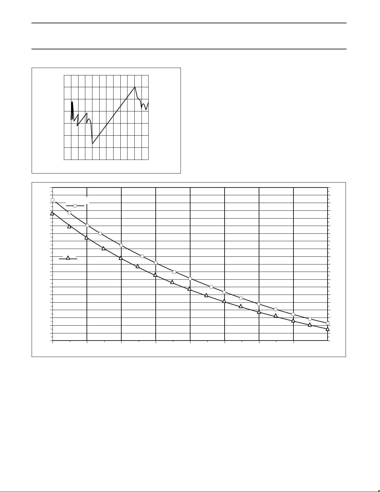
Figure 8. Typical Output Linearity
80
78
76
74
72
70
68
66
64
62
60
58
56
54
52
50
48
46
44
42
40
100
95
90
85
80
75
70
65
60
55
50
0.8 0.9 1.0 1.1 1.2 1.3 1.4 1.5 1.6
Frequency Adjust (kΩ)
I
CC
mA
F
O
MHz
FO MHz
I
CC
SR01045
Figure 9. NE568: Frequency Adjust vs FO and I
CC
Page 7
Philips Semiconductors Product specification
NE/SA568A150MHz phase-locked loop
1996 Feb 1
7
12.0
11.5
11.0
10.5
10.0
9.5
9.0
8.5
8.0
7.5
7.0
6.5
6.0
5.5
5.0
4.5
4.0
3.5
3.0
2.5
2.0
0 10 20 30 40 50 60 70 80 90 100 110 120 130 140 150 160
C = 6.8pF
R
tc
(k )
Ω
FO MHz
C = 16pF
C = 150pF
SR01046
Figure 10. NE568A: Rtc (Pin 13) vs FO; Choosing the Optimum Temperature Compensation Resistor
+5V
V
CC
1
2
3
4
5
6
7
8
9
10
20
19
18
17
16
15
14
13
12
11
C8
0.1µF
C3
0.1µF
C2
18pF
C4
0.1µF
C1
0.1µF
C7
0.1µF
V
CC
2
GND2
GND1
TCAP1
TCAP2
V
CC
1
GND1
REFBYP
PNPBYP
INPBYP
LF1
LF2
LF3
LF4
FREQADJ
V
OUT
OUTFILT
TCADJ2
TCADJ1
V
IN
C5
0.1µF
C6
10µF
GND
J1
+
RFC1
10µH
RFC2
10µH
C13
0.1µF
C12
0.1µF
C10
560pF
C11
47pF
C9
47pF
R1
27Ω
R2
2kΩ
R6
1.5kΩ
R3
43Ω
J3
V
OUT
J2
V
IN
R5
51Ω
R4
3.9kΩ
NE/SA568A
(ZO = 50Ω)*
(Optional. Leave it
open if not used)
(Output Amp Gain
Adj -2dB)
*NOTE: For 75Ω output impedance, use R3 = 68Ω.
SR01113
Figure 11. Phase Locked Loop NE/SA568A
Page 8
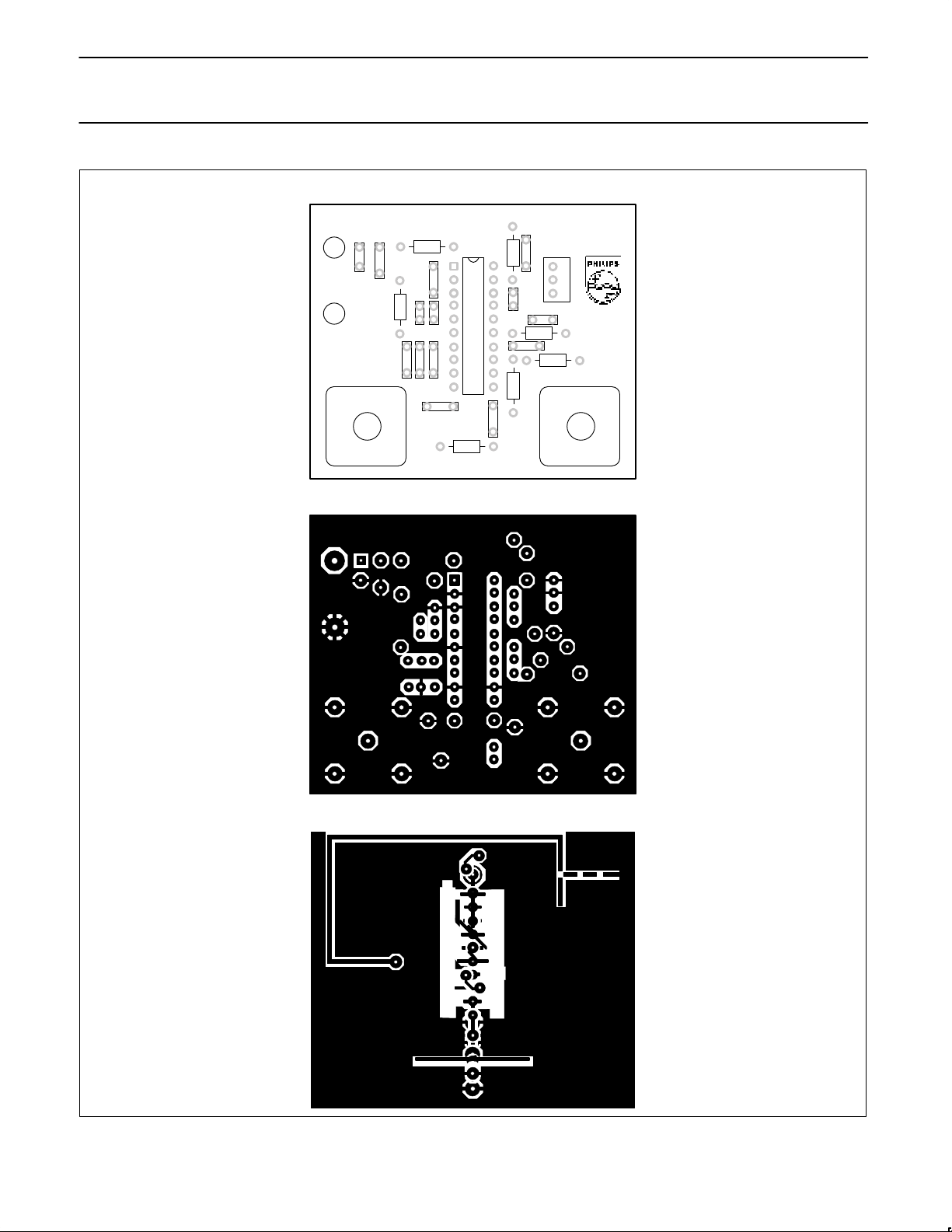
Philips Semiconductors Product specification
NE/SA568A150MHz phase-locked loop
1996 Feb 1
8
C6
C5
RFC2
C2
RFC1
GND
IN
C3
C8C1C4
C7
R5
C13
R4
R3
C12
R6
C11
C9
R2
C10
R1
NE568AN
70MHz
PLL10569
OUT
+5V
TOP
BOTTOM
COMPONENTS LAYOUT
SR01114
Figure 12. NE568AN Board Layout (Not Actual Size)
Page 9
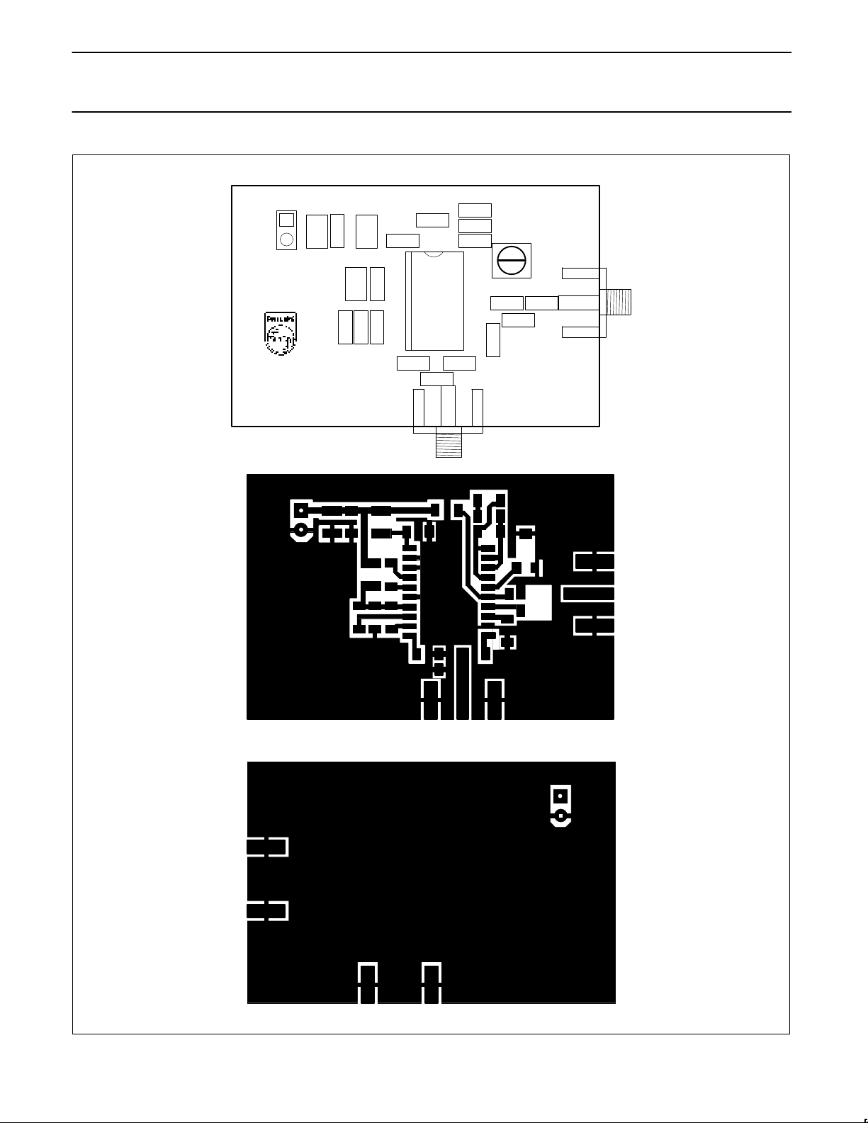
Philips Semiconductors Product specification
NE/SA568A150MHz phase-locked loop
1996 Feb 1
9
VIN
J2
R5
3.9k
C7
C13
NE568AD
70MHz
PLL10570
0.1µF 0.1µF
51
VOUT
J3
0.1µF
R4
C12
R3
47pF 43
C11
R6
R2
2K
C10
560pF
R1
27
47pF
NE568AD
1.5k
C9
U1
C1
0.1µF
C3C8C4
0.1 F
µ
0.1 Fµ0.1 F
µ
+5V
GND
RFC2
J1
C6
C5
RFC1
18pF
10 H
µ
10 H
µ
0.1 F
µ
10 F
µ
SR01115
Figure 13. NE568AD Board Layout (Not Actual Size)
 Loading...