

Page 1

Philips Semiconductors Linear Products Product specification
NE590/591Addressable peripheral drivers
518
August 31, 1994 853-0951 13721
DESCRIPTION
The NE590/591 addressable peripheral drivers are high current
latched drivers, similar in function to the 9334 address decoder. The
device has eight Darlington power outputs, each capable of 250mA
load current. The outputs are turned on or off by respectively loading
a logic high or logic low into the device data input. The required
output is defined by a 3-bit address. The device must be enabled by
a CE
input line. A common clear input, CLR, turns all outputs off
when a logic low is applied.
The NE590 has eight open-collector Darlington outputs which sink
current to ground. The device is packaged in a 16-pin plastic or
Cerdip package.
The NE591 has eight open-emitter Darlington outputs which source
current to an external load from a common collector line, V
S
. This
V
S
line need not necessarily be the same as the 5V VCC supply. The
device is packaged in an 18-pin plastic or Cerdip package.
FEATURES
•8 high current outputs
•Low-loading bus compatible inputs
•Power-on clear ensures safe operation
•NE590 will operate in addressable or demultiplex mode
•Allows random (addressed) data entry
•Easily expandable
•NE590 is pin compatible with 54/74LS259
APPLICATIONS
•Relay driver
•Indicator lamp driver
•Triac trigger
•LED display digit driver
•Stepper motor driver
PIN CONFIGURATIONS
N Package
NE590
N Package
NE591
1
2
3
4
5
6
7
8
9
10
11
12
13
14
16
15
TOP VIEW
1
2
3
4
5
6
7
8
11
12
13
14
15
16
18
17
9
10
A
0
A
1
A
2
Q
0
Q
1
Q
2
Q
3
GND
A
0
A
1
A
2
Q
0
Q
1
Q
2
Q
3
GND
CS
V
CC
CLR
CE
D
Q
7
Q
6
Q
5
Q
4
V
CC
CLR
CE
D
Q
7
Q
6
Q
5
Q
4
V
S
TOP VIEW
ORDERING INFORMATION
DESCRIPTION TEMPERATURE RANGE ORDER CODE DWG #
16-Pin Plastic Dual In-Line Package (DIP) 0 to +70°C NE590N 0406C
18-Pin Plastic Dual In-Line Package (DIP) 0 to +70°C NE591N 0406C
Page 2
Philips Semiconductors Linear Products Product specification
NE590/591Addressable peripheral drivers
August 31, 1994
519
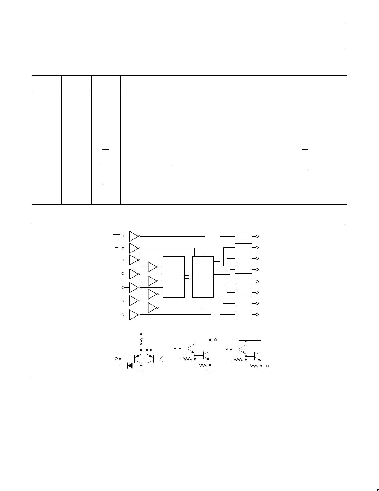
PIN DESIGNATION
590
PIN NO.
591
PIN NO.
SYMBOL NAME & FUNCTION
1-3 2-4 A0-A
2
A 3-bit binary address on these pins defines which of the 8 output latches is to receive the data.
4-7,
9-12
5-8,
11-14
Q0-Q
7
The 8 device outputs. The NE590 has open-collector Darlington outputs. The NE591 has open emitter-follower outputs.
13 15 D The data input. When the chip is enabled, this data bit is transferred to the defined output such that:
“1” turns output switch “ON”
“0” turns output switch “OFF”
Thus in logic terms, the NE590 inverts data to the relevant output. The NE591 retains true data at the
output.
14 16 CE The chip enable. When this input is low, the output latches will accept data. When CE goes high, all
outputs will retain their existing state regardless of address or data input conditions.
15 17 CLR The clear input. When CLR goes low all output switches are turned “OFF”. On the NE590, a high
data input will override the clear function on the addressed latch. On the NE591, CLR
low will over-
ride any other condition.
- 1 CS The chip select input provides for an additional level of address decoding.
- 10 V
S
The VS line provides the power to all 8 output devices. It is connected to the collectors of all 8 output
transistors. This pin may be connected to the V
CC
or another supply.
BLOCK DIAGRAM
LATCH
LATCH
LATCH
LATCH
LATCH
LATCH
LATCH
LATCH
CLR
CE
A
0
A
1
A
2
D
1–OF–8
DECODER
COMTROL
GATE
V
CC
NE590
Q
0
Q
1
Q
2
Q
3
Q
4
Q
5
Q
6
Q
7
cs
(NE51 ONLY)
INPUT STAGE
NE591
OUTPUT STAGE
Page 3
Philips Semiconductors Linear Products Product specification
NE590/591Addressable peripheral drivers
August 31, 1994
520
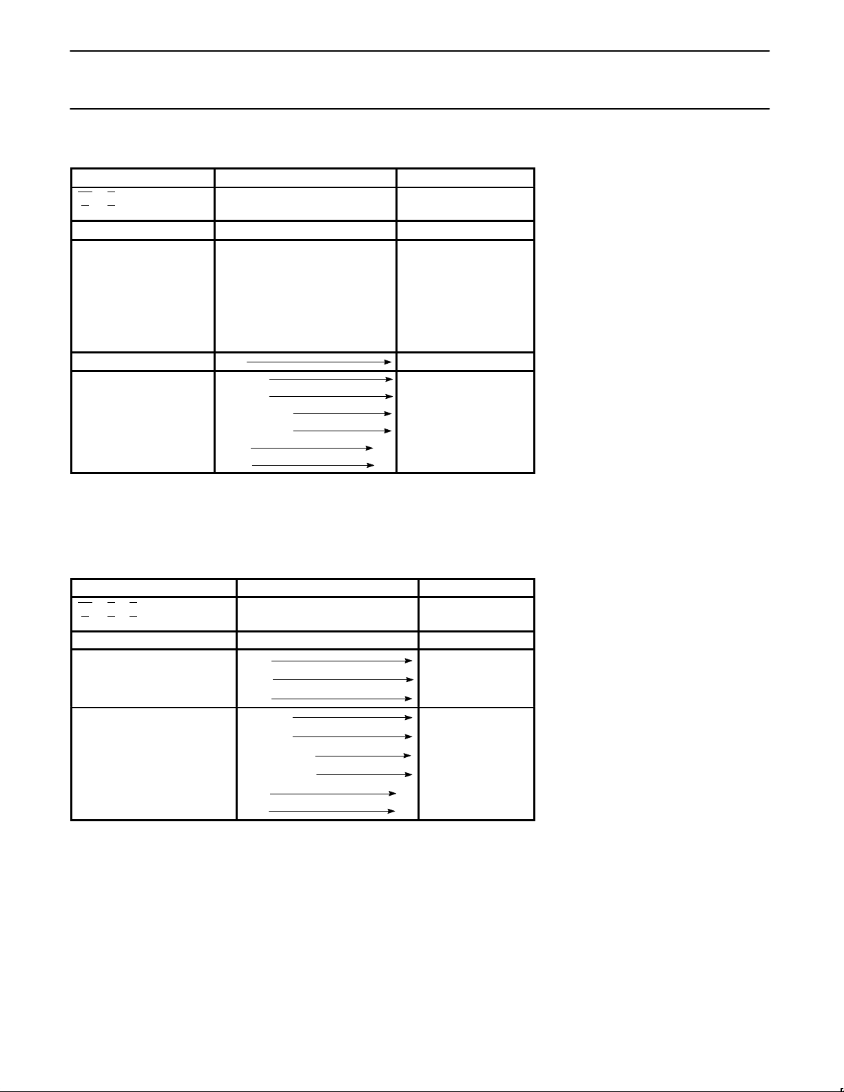
TRUTH TABLE (NE590)
INPUTS OUTPUTS MODE
CLRCED A0A1A2Q0Q1Q2Q3Q4Q5Q6Q
7
L H X X X X H H H H H H H H Clear
L L L L L L H H H H H H H H
L L H L L L L H H H H H H H
L L L H L L H H H H H H H H Demultiplex
L L H H L L H L H H H H H H
L L L H H H H H H H H H H H
L L H H H H H H H H H H H L
H H X X X X Q
N-1
Memory
H L L L L L H Q
N-1
H L H L L L L Q
N-1
H L L H L L Q
N-1
H Q
N-1
Addressable Latch
H L H H L L Q
N-1
L Q
N-1
H L L H H H Q
N-1
H
H L H H H H Q
N-1
L
NOTES:
X=Don’t care condition
Q
N-1
=Previous output state
L=Low voltage level/“OFF” output state
H=High voltage level/“ON” output state
TRUTH TABLE (NE591)
INPUTS OUTPUTS MODE
CLRCECSD A0A1A2Q0Q1Q2Q3Q4Q5Q6Q
7
L X X X X X X L L L L L L L L Clear
H H H X X X X Q
N-1
H H L X X X X Q
N-1
Memory
H L H X X X X Q
N-1
H L L L L L L L Q
N-1
H L L H L L L H Q
N-1
H L L L H L L Q
N-1
L Q
N-1
Addressable Latch
H L L H H L L Q
N-1
H Q
N-1
H L L L H H H Q
N-1
L
H L L H H H H Q
N-1
H
NOTES:
X=Don’t care condition
Q
N-1
=Previous output state
L=Low voltage level/“OFF” output state
H=High voltage level/“ON” output state
Page 4
Philips Semiconductors Linear Products Product specification
NE590/591Addressable peripheral drivers
August 31, 1994
521
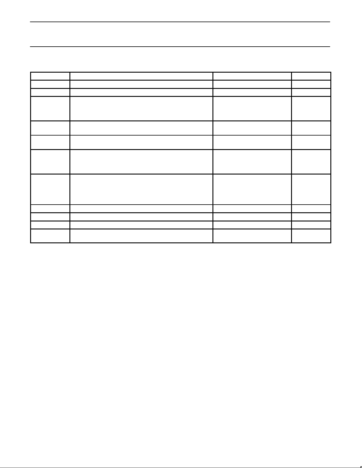
ABSOLUTE MAXIMUM RATINGS
SYMBOL PARAMETER RATING UNIT
V
CC
Supply voltage -0.5 to +7 V
V
IN
Input voltage -0.5 to +15 V
V
OUT
Output voltage V
NE590 0 to +7
NE591 0 to V
CC
V
S
Source bus voltage
NE591 only
-0.5 to +7 V
VS-V
CC
Source/supply differential voltage
NE591 only
-5 to +2 V
I
OUT
Output current
Each output 300 mA
All outputs 1000
P
D
Maximum power dissipation
T
A
=25°C (still air)
NE5901 N package 1450 mW
NE5912 N package 1690
T
A
Ambient temperature range 0 to +70 °C
T
J
Junction temperature 165 °C
T
STG
Storage temperature range -65 to +150 °C
T
SOLD
Lead soldering temperature
(10 sec max)
300 °C
NOTES:
1. Derate above 25°C at the following rates: N package at 11.6mW/°C
2. Derate above 25°C at the following rates: N package at 13.5mW/°C
Page 5
Philips Semiconductors Linear Products Product specification
NE590/591Addressable peripheral drivers
August 31, 1994
522
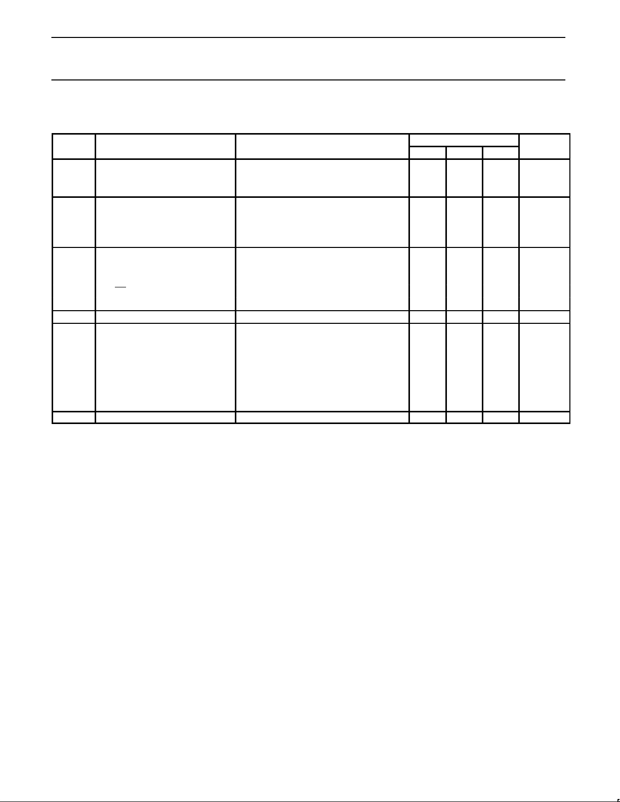
DC ELECTRICAL CHARACTERISTICS
VCC=4.75 to 5.25V, 0°C ≥ T
A
≤ 70°C unless otherwise specified.
1,2
LIMITS
SYMBOL
PARAMETER
TEST CONDITIONS
Min Typ Max
UNIT
Input voltage
V
IH
High 2.0 V
V
IL
Low 0.8
Output voltage
V
OL
Low (NE590 only) IOL=250mA, TA=25°C 1.0 1.3
Over temperature 1.5 V
V
OH
High (NE591 only) IOH=-250mA, VCC=VS=5V 2.9
Input current
I
IH
High VIN=V
CC
0.1 10
I
IL
Low VIN=0V
CE input -25 -60 µA
All other inputs -15 -50
I
OH
Leakage current V
OUT
=5.25V 10 250 µA
Supply current
3
VS=VCC=5V
I
CCL
All outputs low
NE590 33 50
NE591 15 50
I
CCH
All outputs high mA
NE590 15 50
NE591 30 50
P
D
Power dissipation No output load 350 mW
NOTES:
1. All typical values are at V
CC
=5V and TA=25°C
2. For the NE591 V
S=VCC
in all tests.
3. Supply current for the NE591 is measured with no output load.
Page 6
Philips Semiconductors Linear Products Product specification
NE590/591Addressable peripheral drivers
August 31, 1994
523
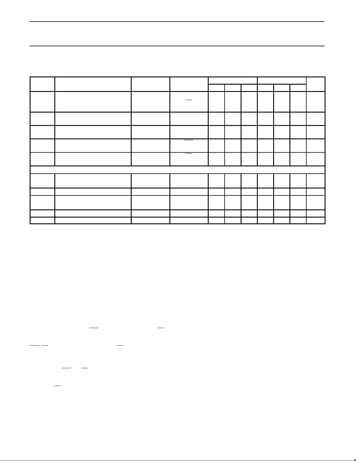
SWITCHING CHARACTERISTICS
V
CC
= 5V, TA = 25°C
NE590 NE591
SYMBOL
PARAMETER
TO
FROM
Min Typ Max Min Typ Max
UNIT
Propagation delay time
t
PLH
t
PHL
Low-to-High
1
High-to-Low
1
Output CE 65
115
150
230
507080
120
ns
t
PLH
t
PHL
Low-to-High
2
High-to-Low
2
Output Data 65
120
130
240
456570
100
ns
t
PLH
t
PHL
Low-to-High
3
High-to-Low
3
Output Address 100
130
200
260
457580
140
ns
t
PLH
t
PHL
Low-to-High
4
High-to-Low
4
Output CLR 65 130
45 140
ns
t
PLH
t
PHL
Low-to-High
1
High-to-Low
1
Output CS 407080
120
ns
Switching setup requirements
t
S(H)
Chip enable High data 210 100 ns
t
S(L)
Chip enable Low data 210 100 ns
t
S(A)
Chip enable Address 30 30 ns
t
H(H)
Chip enable High data 40 10 ns
t
H(L)
Chip enable Low data 30 10 ns
t
S(CS)
Chip enable Low chip select 100 ns
t
PW(E)
Chip enable pulse width
1
120 120 ns
NOTES:
1. See Turn-On and Turn-Off Delays, Enable to Output and Enable Pulse Width timing diagram.
2. See Turn-On and Turn-Off Delays, Data to Output timing diagram.
3. See Turn-On and Turn-Off Delays, Address to Output timing diagram.
4. See Turn-Off Delay, Clear to Output timing diagram.
5. See Setup and Hold Time, Data to Enable timing diagram.
6. See Setup Time, Address to Enable timing diagram.
FUNCTIONAL DESCRIPTION
These peripheral drivers have latched outputs which hold the input
data until cleared. The NE590 has active-Low, open-collector
outputs, while the NE591 has active-High, uncommitted (open)
emitter outputs. All outputs are cleared when power is first applied.
Addressable Latch Function
Any given output can be turned on or off by presenting the address
of the output to be set or cleared to the three address pins, by
holding the “D” input High to turn on the selected input, or by holding
it Low to turn off, holding the CLR
input High, and bringing the CE
input Low. Once an output is turned on or off, it will remain so until
addressed again, or until all outputs are cleared by bringing the
CLR
, CE, and “D” inputs Low. For NE591, CS must be brought Low
any time CE is Low if any outputs are to be changed.
Demultiplexer Operation
By bringing the CLR and CE inputs Low and the “D” input High, the
addressed output will remain on and all other outputs will be off. This
condition will remain only as long as the output is addressed. For the
NE591, the CS
input must also be Low.
High Current Outputs
The obvious advantage of these devices over the 9334 and
N74LS259 (which provide a similar function) is the fact that the
NE590 and NE591 are capable of output currents of 250mA at each
of their eight outputs. It should be noted, however, that the load
power dissipation would be over 2.5W if all 8 outputs were to carry
their full rated load current at one time. Since the total power
dissipation is limited by the package to 1W, and since the power
dissipation due to supply current is 0.25W, the total load power
dissipation by the device is limited to 0.75W, and decreases as
ambient temperature rises.
The maximum die junction temperature must be limited to 165°C,
and the temperature rise above ambient and the junction
temperature are defined as:
t
R=θJA
×P
t
J=tA+tR
where
θ
JA
is die junction to ambient thermal resistance.
P
D
is total power dissipation
t
R
is junction temperature rise above ambient
t
j
is die junction temperature
t
A
is ambient (surrounding medium) temperature
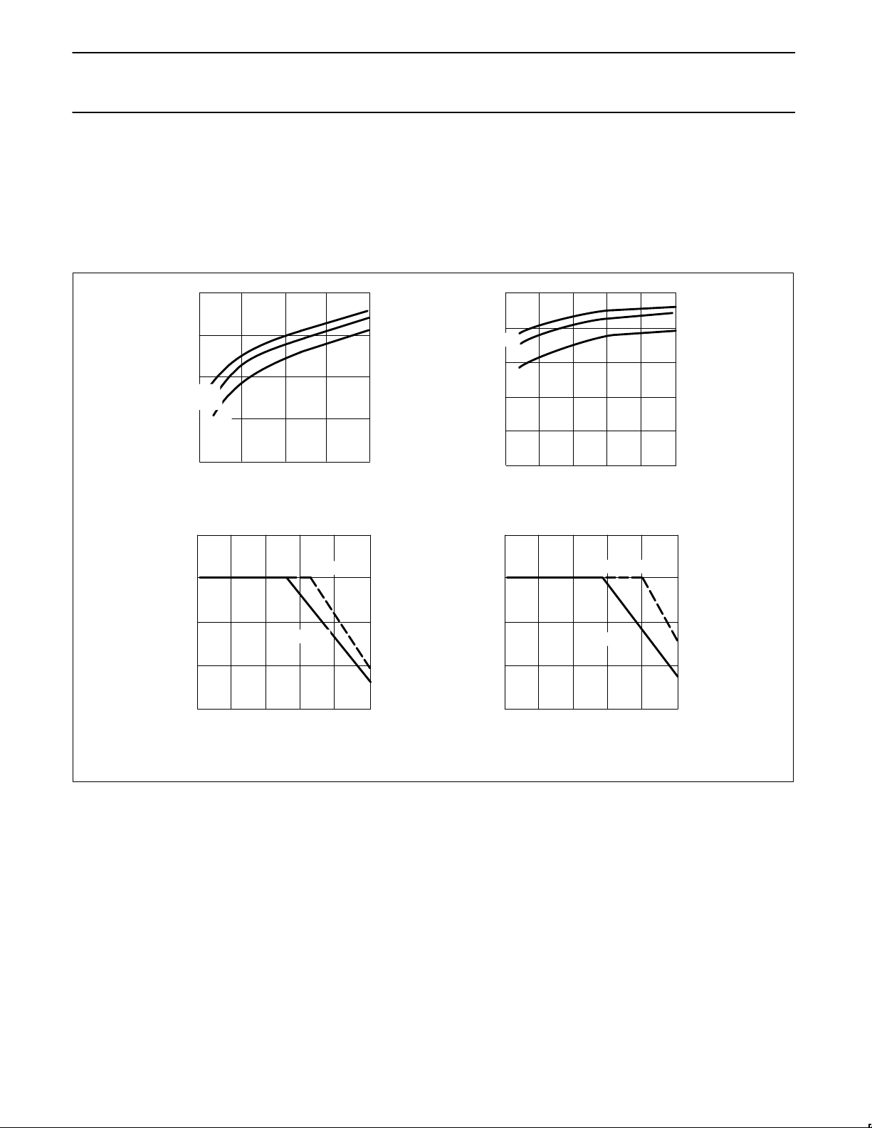
For example, if we are using the NE590 in a plastic package in an
application where the ambient temperature is never expected to rise
above 50°C, and the output current at the 8 outputs, when on, are
100, 40, 50, 200, 15, 30, 80, and 10mA, we find from the graph of
output voltage vs load current that the output voltages are expected
to be about 0.92, 0.75, 0.78, 1.04, 0.5, 0.7, 0.9, and 0.4V ,
respectively. Total device power due to these loads is found to be
473.5mW. Adding the 250mW due to the power supply brings total
device power dissipation to 723.5mW. The thermal resistances are
83°C per W for plastic packages and 100°C per W for Cerdips.
Using the equations above we find:
Page 7
Philips Semiconductors Linear Products Product specification
NE590/591Addressable peripheral drivers
August 31, 1994
524
Plastic t
R
=83×0.7235=60°C
Plastic t
J
=50+60=100°C
Cerdip t
R
=100×0.7235=72.40°C
Cerdip t
J
=50+72.4=122.4°C
Thus we find that t
J
for either package is below the 165°C maximum
and either package could be used in this application. The graphs of
total load power vs ambient temperature would also give us this
same information, although interpreting the graphs would not yield
the same accuracy.
TYPICAL PERFORMANCE CHARACTERISTICS
TOTAL LOAD POWER (W)
N PACKAGE
F PACKAGE
0 25 50 75 100 125
1.0
0.75
0.50
0.25
TEMPERATURE (
o
C)
Output Voltage vs Load Current
(NE590)
Output Voltage Drop vs Load Current
(NE591)
Total Load Power vs Temperature
(NE590)
Total Load Power vs Temperature
(NE591)
OUTPUT VOLTAGE (V)
TOTAL LOAD POWER (W)
1.2
1.0
0.8
0.6
0.4
0
50
100
150
200
70 C
25 C
0 C
N PACKAGE
F PACKAGE
0 25 50 75 100 125
1.0
0.75
0.50
0.25
OUTPUT LOAD CURRENT (mA)
TEMPERATURE (
o
C)
OUTPUT VOLTAGE (V –V )
2.0
1.8
1.6
0 50 100 150 200
70 C
25 C
0 C
OUTPUT LOAD CURRENT (mA)
CC
O
1.0
1.2
1.4
250
Page 8
Philips Semiconductors Linear Products Product specification
NE590/591Addressable peripheral drivers
August 31, 1994
525
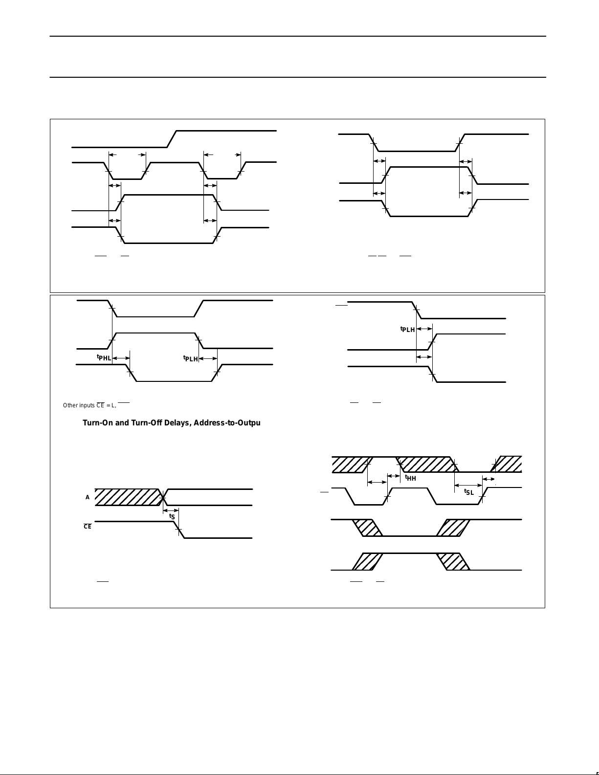
TIMING DIAGRAMS
t
PHL
t
PLH
t
PLH
t
PHL
t
PHL
t
PLH
t
PHL
t
PLH
Turn-On and Turn-Off Delays, Enable-to-Output
and Enable Pulse Width
Turn-On and Turn-Off Delays, Data-to-Output
NOTE:
Other inputs CE CS = L, CLR = H, A = Stable
NOTE:
Other inputs CLR = H, CS = L, A = Stable
D
CE
Q (NE590)
t
PW
t
PW
Q (NE591)
D
Q (NE590)
Q (NE590)
ÉÉÉ
ÉÉÉ
ÉÉÉ
t
SL
t
HH
t
S
A
CE
t
PLH
t
PHL
t
PLH
Turn-On and Turn-Off Delays, Address-to-Output
NOTE:
Other inputs CE
= L, CLR = L, D = H
Turn-On and Turn-Off Delays, Clear-to-Output
NOTE:
Other inputs CS
= H, CE = H
Set-Up Time, Address-to-Enable
NOTE:
Other inputs CLR = H, CS = L
Set-Up and Hold Time, Data-to-Enable
NOTE:
Other inputs CLR = H, CS = L, A = Stable
A
A
Q (NE590)
CLR
Q (NE590)
Q (NE591)
t
PHL
D
CE
Q (NE590)
t
SH
t
HL
Q (NE591)
ÉÉÉ
ÉÉÉ
ÉÉÉ
Page 9
Philips Semiconductors Linear Products Product specification
NE590/591Addressable peripheral drivers
August 31, 1994
526
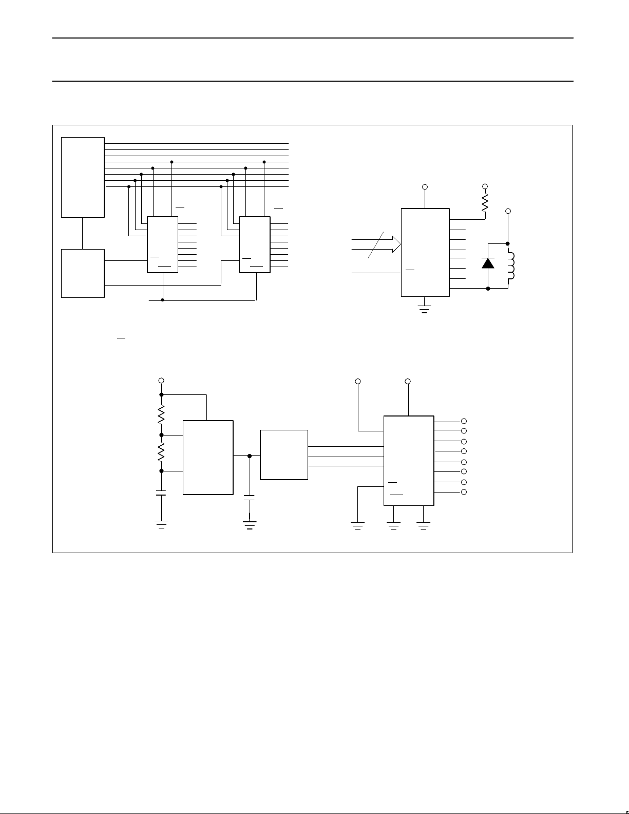
TYPICAL APPLICATIONS
590
Q
0
Q
1
Q
2
Q
3
Q
0
Q
5
Q
6
Q
7
+ 5V
+5V
+6V
4
CE
R
L
NE590 Operating in Demultiplex Mode
Turn-On and Turn-Off Delays, Address-to-Output
NOTE:
A
0
, A1, A2, and CS may be connected to the address bus if permitted by system design.
NE590 Driving Simple Loads
µP
D
A
2
A
1
A
0
590 1
D
A
2
A
1
A
0
590/1
Q
0
Q
1
Q
2
Q
3
Q
0
Q
5
Q
6
Q
7
Q
0
Q
1
Q
2
Q
3
Q
0
Q
5
Q
6
Q
7
CLEAR
IQ
CONTROL
CE
CLR
CE
CLR
DATA
BUS
CS
(591 ONLY)
CS
(591 ONLY)
RELAY
LOAD
3–BIT
COUNTER
+5V
555
+5V +5V
Q
0
Q
1
Q
2
Q
3
Q
0
Q
5
Q
6
Q
7
D
A
0
A
1
A
2
CE
590
CLR
 Loading...