

SGS Thomson Microelectronics M50LPW002 Datasheet
3V Supply Low Pin Count Flash Memory
FEATURES SUMMARY
■ SUPPLY VOLTAGE
= 3 V to 3.6 V for Program, Erase and
–V
CC
Read Operations
–V
= 12 V for Fast Program and Fast Erase
PP
(optional)
■ TWO INTERFACES
– Low Pin Count (LPC) Standard Interface for
embedded operation with PC Chipsets.
– Address/Address Multiplexed (A/A Mux)
Interface for programming equipment
compatibility.
■ LOW PIN COUNT (LPC) HARDWARE
INTERFACE MODE
– 5 Signal Communication Interface supporting
Read and Write Operations
– Hardware Write Protect Pins for Block
Protection
– Register Based Read and Write Protection
– 5 Additional General Purpose Inputs for
platform design flexibility
– Synchronized with 33 MHz PCI clock
■ PROGRAMMING TIME
– 10 µs typical
– Quadruple Byte Programming Option
■ 7 MEMORY BLOCKS
– 1 Boot Block (Top Location)
– 4 Main Blocks and 2 Parameter Blocks
■ PROGRAM/ERA SE CON T ROL LER
– Embedded Byte Program, Block Erase and
Chip Erase algorithms
– Status Register Bits
■ PROGRAM and ERASE SUSPEND
– Read other Blocks during Program/Erase
Suspend
– Program other Blocks during Erase Suspend
■ FOR USE in PC BIOS APPLICATIONS
M50LPW002
2 Mbit (256Kb x8, Boot Block)
PRELIMINARY DATA
Figure 1. Packages
PLCC32 (K)
■ ELECTRONIC SIGNATURE
– Manufacturer Code: 20h
– Device Code: 31h
May 2002
This is preliminary information on a new product now in development or undergoing evaluation. Details are subject to change without notice.
1/39

M50LPW002
TABLE OF CONTENTS
SUMMARY DESCRIPTION. . . . . . . . . . . . . . . . . . . . . . . . . . . . . . . . . . . . . . . . . . . . . . . . . . . . . . . . . . . 4
SIGNAL DESCRIPTIONS . . . . . . . . . . . . . . . . . . . . . . . . . . . . . . . . . . . . . . . . . . . . . . . . . . . . . . . . . . . . 6
Low Pin Count (LPC) Signal Descriptions . . . . . . . . . . . . . . . . . . . . . . . . . . . . . . . . . . . . . . . . . . 6
Address/Address M ultiplexe d (A/A Mux) Sign al Descrip tions . . . . . . . . . . . . . . . . . . . . . . . . . . 7
Supply Signal Description s . . . . . . . . . . . . . . . . . . . . . . . . . . . . . . . . . . . . . . . . . . . . . . . . . . . . . . 7
Memory Identification Input Configuration. . . . . . . . . . . . . . . . . . . . . . . . . . . . . . . . . . . . . . . . . . . . . 8
BUS OPERATIONS. . . . . . . . . . . . . . . . . . . . . . . . . . . . . . . . . . . . . . . . . . . . . . . . . . . . . . . . . . . . . . . . . 9
Low Pin Count (LPC) Bus Operations. . . . . . . . . . . . . . . . . . . . . . . . . . . . . . . . . . . . . . . . . . . . . . 9
Bus Read Field Definitions (LPC Interface). . . . . . . . . . . . . . . . . . . . . . . . . . . . . . . . . . . . . . . . . . . 10
Bus Write Field Definitions (LPC Interface). . . . . . . . . . . . . . . . . . . . . . . . . . . . . . . . . . . . . . . . . . .11
Address/Address M ultiplexe d (A/A Mux) B us Operati ons. . . . . . . . . . . . . . . . . . . . . . . . . . . . . 12
A/A Mux Bus Operations. . . . . . . . . . . . . . . . . . . . . . . . . . . . . . . . . . . . . . . . . . . . . . . . . . . . . . . . . 12
Manufacturer and Device Codes. . . . . . . . . . . . . . . . . . . . . . . . . . . . . . . . . . . . . . . . . . . . . . . . . . . 12
Commands . . . . . . . . . . . . . . . . . . . . . . . . . . . . . . . . . . . . . . . . . . . . . . . . . . . . . . . . . . . . . . . . . . . 13
COMMAND INTERFACE . . . . . . . . . . . . . . . . . . . . . . . . . . . . . . . . . . . . . . . . . . . . . . . . . . . . . . . . . . . 14
STATUS REGISTER. . . . . . . . . . . . . . . . . . . . . . . . . . . . . . . . . . . . . . . . . . . . . . . . . . . . . . . . . . . . . . . 16
Status Register Bits. . . . . . . . . . . . . . . . . . . . . . . . . . . . . . . . . . . . . . . . . . . . . . . . . . . . . . . . . . . . . 17
LOW PIN COUNT (LPC) INTERFACE CONFIGURATION REGISTERS. . . . . . . . . . . . . . . . . . . . . . . 18
Lock Registers. . . . . . . . . . . . . . . . . . . . . . . . . . . . . . . . . . . . . . . . . . . . . . . . . . . . . . . . . . . . . . . . 18
General Purpose Input Register. . . . . . . . . . . . . . . . . . . . . . . . . . . . . . . . . . . . . . . . . . . . . . . . . .18
Low Pin Count Register Configuration Map
(1)
Lock Register Bit Definitions
. . . . . . . . . . . . . . . . . . . . . . . . . . . . . . . . . . . . . . . . . . . . . . . . . . . . 19
General Purpose Input Register Definition
(1)
. . . . . . . . . . . . . . . . . . . . . . . . . . . . . . . . . . . . . . . . 18
(1)
. . . . . . . . . . . . . . . . . . . . . . . . . . . . . . . . . . . . . . . . . . 19
MAXIMUM RATING. . . . . . . . . . . . . . . . . . . . . . . . . . . . . . . . . . . . . . . . . . . . . . . . . . . . . . . . . . . . . . . . 20
Absolute Maximum Ratings. . . . . . . . . . . . . . . . . . . . . . . . . . . . . . . . . . . . . . . . . . . . . . . . . . . . . . . 20
DC and AC PARAMETERS . . . . . . . . . . . . . . . . . . . . . . . . . . . . . . . . . . . . . . . . . . . . . . . . . . . . . . . . . 2 1
Operating Conditions. . . . . . . . . . . . . . . . . . . . . . . . . . . . . . . . . . . . . . . . . . . . . . . . . . . . . . . . . . . . 21
AC Measurement Conditions (LPC Interface). . . . . . . . . . . . . . . . . . . . . . . . . . . . . . . . . . . . . . . . . 21
AC Measurement Conditions (A/A Mux Interface). . . . . . . . . . . . . . . . . . . . . . . . . . . . . . . . . . . . . .22
Device Impedance. . . . . . . . . . . . . . . . . . . . . . . . . . . . . . . . . . . . . . . . . . . . . . . . . . . . . . . . . . . . . . 22
DC Characteristics. . . . . . . . . . . . . . . . . . . . . . . . . . . . . . . . . . . . . . . . . . . . . . . . . . . . . . . . . . . . . . 23
Clock Characteristics (LPC Interface) . . . . . . . . . . . . . . . . . . . . . . . . . . . . . . . . . . . . . . . . . . . . . . . 24
AC Signal Timing Characteristics (LPC Interface) . . . . . . . . . . . . . . . . . . . . . . . . . . . . . . . . . . . . . . 25
Program and Erase Times. . . . . . . . . . . . . . . . . . . . . . . . . . . . . . . . . . . . . . . . . . . . . . . . . . . . . . . . 26
2/39

M50LPW002
Reset AC Characteristics . . . . . . . . . . . . . . . . . . . . . . . . . . . . . . . . . . . . . . . . . . . . . . . . . . . . . . . . 2 6
Read AC Characteristics (A/A Mux Interface) . . . . . . . . . . . . . . . . . . . . . . . . . . . . . . . . . . . . . . . . . 28
Write AC Characteristics (A/A Mux Interface) . . . . . . . . . . . . . . . . . . . . . . . . . . . . . . . . . . . . . . . . . 29
PACKAGE MECHANICAL . . . . . . . . . . . . . . . . . . . . . . . . . . . . . . . . . . . . . . . . . . . . . . . . . . . . . . . . . . 3 6
PLCC32 – 32 lead Plastic Leaded Chip Carrier, Package Mechanical Data . . . . . . . . . . . . . . . . . 36
PART NUMBERING . . . . . . . . . . . . . . . . . . . . . . . . . . . . . . . . . . . . . . . . . . . . . . . . . . . . . . . . . . . . . . . 37
Ordering Information Scheme . . . . . . . . . . . . . . . . . . . . . . . . . . . . . . . . . . . . . . . . . . . . . . . . . . . . . 37
REVISION HISTORY. . . . . . . . . . . . . . . . . . . . . . . . . . . . . . . . . . . . . . . . . . . . . . . . . . . . . . . . . . . . . . . 38
Document Revision History. . . . . . . . . . . . . . . . . . . . . . . . . . . . . . . . . . . . . . . . . . . . . . . . . . . . . . . 38
3/39
M50LPW002
SUMMARY DESCRIPTION
The M50LPW002 is a 2 Mbit (256Kb x8) non-volatile memory that can be read, erased and reprogrammed. These operations can be performed
using a single low voltage (3.0 to 3.6V) supply. For
fast programming and fast erasing in production
lines an optional 12V power supply can be used to
reduce the programming and the erasing times.
The memory is divided into blocks that can be
erased independently so it is pos sible to pres erve
valid data while old data is erased. Blocks can be
protected individually to prevent accidental Program or Erase commands from modifying the
memory. Program and Erase com m ands are wri tten to the Command Interface of t he memory. An
on-chip Program/Erase Controller simplifies the
process of programming or erasing the memory by
taking care of all of the special operations that are
required to update the memory contents. The end
of a program or erase op eration can be de tected
and any error conditions identified. The command
set required to control the memory is consistent
with JEDEC standards.
The device features an asymmetrical blocked architecture. The device has an array of 7 blocks:
■ 1 Boot Block of 16 KByte
■ 2 Parameter Blocks of 8 KByte each
■ 1 Main Block of 32 KByte
■ 3 Main Blocks of 64 KByte each
Two different bus interfaces are supported by t he
memory. The primary interface is the Low Pin
Count (or LPC) Standard Interface. This has been
designed to remove the need for the ISA bus in
current PC Chipsets; the M50LPW002 acts as the
PC BIOS on the Low P in Count bus for these P C
Chipsets.
The secondary interface, the Address/Address
Multiplexed (or A/A Mux) Int erface, is design ed t o
be compatible with current Flash Programmers for
production line programming prior to fitting to a PC
Motherboard.
The memory is delivered with al l the bits erased
(set to 1).
Figure 2. PLCC Connections
A/A Mux A/A Mux
A7
A6
A5
A4
A3
A2
A1
A0
DQ0
GPI1
GPI0
WP
TBL
ID3
ID2
ID1
ID0
LAD0
GPI2
9
LAD1
DQ1
RPA8VPPV
A9
RP
VPPV
GPI3
1
32
M50LPW002
17
SS
V
V
SS
RFU
LAD3
DQ3
DQ4
LAD2
DQ2
CC
CC
RC
CLK
RFU
DQ5
A10
GPI4
25
RFU
DQ6
IC (VIL)
NC
NC
V
SS
V
CC
INIT
LFRAME
RFU
RFU
IC (VIH)
NC
NC
V
SS
V
CC
G
W
RB
DQ7
A/A MuxA/A Mux
AI05744
Note: Pi ns 27 and 28 are not interna l l y co nnected.
4/39
M50LPW002
Figure 3. Logic Diagram (LPC Interface)
V
ID0-ID3
GPI0-
GPI4
LFRAME
CLK
IC
RP
INIT
V
4
5
M50LPW002
V
CC
SS
PP
4
LAD0LAD3
WP
TBL
AI05742
Figure 4. Logic Diagram (A/A Mux Interface)
V
A0-A10
RC
IC
W
RP
V
11
M50LPW002
G
V
CC
SS
PP
8
DQ0-DQ7
RB
AI05743
Table 1. Signal Names (LPC Interface)
LAD0-LAD3 Input/Output Communications
LFRAME
ID0-ID3 Identification Inputs
GPI0-GPI4 General Purpose Inputs
IC Interface Configuration
RP
INIT
CLK Clock
TBL
WP
RFU
V
CC
V
PP
Input Communication Frame
Interface Reset
CPU Reset
Top Block Lock
Write Protect
Reserved for Future Use. Leave
disconnected
Supply Voltage
Optional Supply Voltage for Fast
Erase Operations
Table 2. Signal Names (A/A Mux Interface)
IC Interface Configuration
A0-A10 Address Inputs
DQ0-DQ7 Data Inputs/Outputs
G
W
RC
RB
RP
V
CC
V
PP
V
SS
NC Not Connected Internally
Output Enable
Write Enable
Row/Column Address Select
Ready/Busy Output
Interface Reset
Supply Voltage
Optional Supply Voltage for Fast
Program and Fast Erase Operations
Ground
V
SS
NC Not Connected Internally
Ground
5/39

M50LPW002
SIGNAL DESCRIPTIONS
There are two different bus interfaces available on
this part. The active interface is selected before
power-up or during Reset using the Interface Configur a tion Pin, IC.
The signals for each interface are discussed in the
Low Pin Count (LPC) Signal Descriptions section
and the Address/Address M ultiplexed (A/A Mux)
Signal Descriptions section below. The supply signals are discussed in the Supply S ignal Descriptions section below.
Low Pin Count (LPC) Signal Descriptions
For the Low Pin Count (LPC) Interface see Figure
3, Logic Diagram, and Table 1, Signal Names.
Input/Output Communications (LAD0-LAD3). All
Input and Output Communication with the memory
take place on these pi ns. Addresses and Data for
Bus Read and Bus W rite operations are en coded
on these pins.
Input Communication Frame (LFRAME
Input Communication Frame (LFRAME
the start of a bus operation. When Input Communication Frame is Low, V
, on the rising edge of
IL
the Clock a new bus operat ion is in itiated. If Input
Communication Frame is L ow, V
IL
operation then the operation is aborted. When Input Communication Frame is High, V
rent bus operation is proceeding or the bus is idle.
Identification Inputs (ID0-ID3). The Identification
Inputs (ID0-ID3) allow to address up to 16
memories on a bus. The value on addresses A18A21 is compared to the hardware strapping on the
ID0-ID3 pins to select which memory is being
addressed. For an address bit to be ‘1’ the
correspondent ID pin c an be left floating or driven
Low, VIL; an internal pull-down resistor is included
with a value of R
. For an address bit to be ‘0’ the
IL
correspondent ID pin must be driven High, V
there will be a leakage current of I
pin when pulled to V
; see Table 20.
IH
LI2
By convention t he boot memory must h ave ID0ID3 pins left floating or driven Low, V
‘1111’ value on A18-A21 and all additional
memories take sequential ID0-ID3 configuration,
as shown in Table 3.
General Purpose Inputs (GPI0-GPI4). The General Purpose Inputs can be used as digital inputs for
the CPU to read. The General Purpose Input Register holds the values on these pins. The pins must
have stable data from before the start of the cycle
that reads the General Purpose Input Register until after the cycle is complete. These pins must not
be left to float, they should be driven Low, V
High, V
.
IH
Interface Configuration (IC). The Interface Configuration input selects whether the Low Pin Count
(LPC) or the Address/Address Multiplexed (A/A
). The
) signals
, during a bus
, the cur-
IH
IH
through each
and a
IL
or
IL,
Mux) Interface is used. The chosen interface must
be selected before power-up or during a Reset
and, thereafter, cannot be change d. The state of
the Interface Configuration, IC, should not be
changed during operation.
To select the Low Pin Count (LPC) Interface the
Interface Configuration pin should be left to float or
driven Low, V
; to select the Address/Address
IL
Multiplexed (A/A Mux) Interface t he pin should be
driven High, V
included with a value of R
current of I
. An internal pull-down resistor is
IH
through each pin when pulled to VIH;
LI2
; there will be a leakage
IL
see Table 20.
Interface Reset (RP
). The Interface Reset (RP)
input is used to reset the memory. When Interface
Reset (RP
) is set Low, VIL, the memor y i s i n R ese t
mode: the outputs are put to high impedance and
the current consumption is minimized. When RP
set High, V
, the memory is in no rmal operat ion.
IH
After exiting Reset mode, the memory enters
Read mode.
CPU Reset (INIT
). The CPU Reset, INIT, pin is
used to Reset the memory when the CPU is reset .
It behaves identically to Interface Reset, RP
the internal Reset lin e is the logical OR (elec tric al
AND) of RP
and INIT.
Clock (CLK). The Clock, CLK, input is used to
clock the signals in and out of the Input/Output
Communication Pins, LAD0-LAD3. The Clock
conforms to the PCI specification.
Top Block Lock (TB L
). The Top Block Lock
input is used to pre vent the Top Block (Block 6)
from being chan ged. When Top Block Loc k, TBL
is set Low, V
, Program and Erase operations in
IL
the Top Block have no effect, regardless of the
state of the Lock Register. When To p Bloc k Loc k,
, is set High , VIH, the protection of the Block is
TBL
;
determined by the Lock Register. The state of Top
Block Lock, TBL
, does not affect the protection of
the other blocks (Blocks 0 to 5).
Top Block Lock, TBL
, must be set prior to a Program or Erase operation is initiated and must not
be changed until the o peration completes or unpredictable results may occur. Care should be taken to avoid unpredictable behavior by changing
TBL
during Program or Erase Suspend.
Write Protect (WP
). The Write Protect input is
used to prevent the blocks 0 to 5 from being
changed. When Write Protect, WP
, is s et Lo w, VIL,
Program and Erase operations in these blocks
have no effect, regardless of the state of the Lock
Register. When Write Protect, WP
, the protection of the block is determined by
V
IH
, is set High,
the Lock Regist er. T he st ate of Write Prot ect, WP
does not affect the protection of the Top Block
(Block 6).
is
, and
,
,
6/39

M50LPW002
Write Protect, WP, must be set prior to a Program
or Erase operation is initiated and must not be
changed until the operation completes or unpredictable results may occur. Care should be taken
to avoid unpredictable behavior by changing WP
during Program or Erase Suspend.
Reserved for Future Use (RFU). These pins do
not have assigned func tions i n this revision of the
part. They must be left disconnected.
Address/Address Multiplexed (A/A Mux)
Signal Descriptions
For the Address/Address Multiplexed (A/A Mux)
Interface see Figure 4, Logic Diagram, and Table
2, Signal Names.
Address Inputs (A0-A10). The Address Inputs
are used to set the Row Address bits (A0-A10) and
the Column Address bits (A11-A17). They are
latched during any bus operation by the Row/ Column Address Select input, RC
.
Data Inputs/Outputs (DQ0-DQ7). The Data Inputs/Outputs hold the data that is written to or read
from the memory. They output the data s tored at
the selected address during a Bus Read operation. During Bus Write operations they represent
the commands sent t o the Command Interface of
the internal state machine. The Data I nputs/Outputs, DQ0-DQ7, are latched during a Bus Write
operation.
Output Enable (G
). The Output Enable, G, con-
trols the Bus Read operation of the memory.
Write Enable (W
). The Write Enable, W, controls
the Bus Write operation of the memory’s Command Interf a c e .
Row/Column Address Select (RC
). The Row/
Column Address Select input selects whether the
Address Inputs should be latched into the Row
Address bits (A0-A10) or the Column Address bits
(A11-A17). The Row Address bits are latched on
the falling edge of RC
whereas the Column
Address bits are latched on the rising edge.
Ready/Busy Output (RB
). The Ready/Busy pin
gives the status of the memory’s Program/Erase
Controller. When Ready/Busy is Low, V
OL
, the
memory is busy with a Program or Erase operation
and it will not accept any additional Program or
Erase command except the Program/Erase
Suspend command. When Ready/Busy is High,
V
, the memory is ready for any Rea d, Program
OH
or Erase operation.
Supply Signal Descriptions
The Supply Signals are the same for both interfaces.
Supply Voltage. The VCC Supply Voltage
V
CC
supplies the power for all operations (Read, Program, Erase etc.).
The Command Interface is disabled when the V
CC
Supply Voltage is less than the L ockout Voltage,
V
. This prevents Bus Write operations from
LKO
accidentally damaging the data during power up,
power down and power surges. If the Program/
Erase Controller is programming or erasing during
this time then the operation aborts and the
memory contents being altered will be invalid.
After V
becomes valid the Comma nd Interface
CC
is reset to Read mode.
A 0.1µF capacitor should be connected between
the V
Supply Voltage pins and the VSS Ground
CC
pin to decouple the current surges from the power
supply. Both V
Supply Voltage pins must be
CC
connected to the power supply. The PCB track
widths must be sufficient to carry the currents
required during program and erase operations.
Optional Supply Voltage. The VPP Optional
V
PP
Supply Voltage pin is used to select the Fast
Program (see the Quadruple Byte Program
Command description) and Fast Erase options of
the memory and to protect the memory. When V
< V
Program and Erase operations cannot be
PPLK
PP
performed and an error is reported in the Sta tus
Register if an attempt to change the memory
contents is made. When V
= VCC Program and
PP
Erase operations take place as normal. When
V
PP
= V
Fast Program (if a Quadruple Byte
PPH
Program Command is performed ) and Fast Erase
operations are used. Any other voltage input to
will res ult in undefined beha vior and should
V
PP
not be used.
V
should not be set to V
PP
for more than 80
PPH
hours during the life of the memory.
V
Ground. VSS is the reference for al l the vol t-
SS
age measurements.
7/39
M50LPW002
Table 3. Memory Identification Input Configuration
Memory Number ID3 ID2 ID1 ID0 A21 A20 A19 A18
V
1 (Boot)
2
3
4
5
6
7
8
9
10
11
12
13
14
15
16
or floating VIL or floating VIL or floating VIL or floating
IL
V
or floating VIL or floating VIL or floating V
IL
V
or floating VIL or floating V
IL
V
or floating VIL or floating V
IL
V
or floating V
IL
V
or floating V
IL
V
or floating V
IL
V
or floating V
IL
V
IH
V
IH
V
IH
V
IH
V
IH
V
IH
V
IH
V
IH
IH
IH
IH
IH
VIL or floating VIL or floating VIL or floating
VIL or floating VIL or floating V
VIL or floating V
VIL or floating V
V
IH
V
IH
V
IH
V
IH
IH
IH
VIL or floating VIL or floating
VIL or floating V
V
IH
V
IH
IH
IH
VIL or floating VIL or floating
VIL or floating V
V
IH
V
IH
VIL or floating
V
VIL or floating
V
VIL or floating
V
VIL or floating
V
1111
IH
1110
1101
IH
1100
1011
IH
1010
1001
IH
1000
0111
IH
0110
0101
IH
0100
0011
IH
0010
0001
IH
0000
Table 4. Block Addresses
Size
(Kbytes)
Address Range
16 3C000h-3FFFFh 6
8 3A000h-3BFFFh 5
8 38000h-39FFFh 4
32 30000h-37FFFh 3 Main Block
64 20000h-2FFFFh 2 Main Block
64 10000h-1FFFFh 1 Main Block
64 00000h-0FFFFh 0 Main Block
Note: For A18 and A19 values, ref er to Table 3.
8/39
Block
Number
Block Type
Boot Block
Parameter
Parameter
(Top)
Block
Block

BUS OPERATIONS
The two interfaces have similar bus operations but
the signals and tim ings are comple tely different.
The Low Pin Count (LPC) In terface is the usual
interface and all of the functionality of the part is
available through this interfac e. Only a subset of
functions are available through the Address/
Address Multiplexed (A/A Mux) Interface.
Follow the section Low Pin Count (LPC) Bus
Operations below and the section Address/
Address Multiplexed (A/A Mux) Interface Bus
Operations below for a description of the bus
operations on each interface.
Low Pin Count (LPC) Bus Operations
The Low Pin Count (LPC) Interface consists of
four data signals (LAD0-LAD3), one control line
(LFRAME
) and a clock (CLK). In addition
protection against accidental or malicious data
corruption can be achieved using two further
signals (TBL
(RP
and INIT) are available to put the memory into
and WP). Finally two reset signals
a known state.
The data signals, control signal and clock are
designed to be compatible with PCI electrical
specifications. The interface operates with clock
speeds up to 33MHz.
The following operations can be performed using
the appropriate bus cycles: Bus Read, Bus Write,
Standby, Reset and Block Protection.
Bus Read. Bus Read operations read from the
memory cells, specific registers in the Command
Interface or Low Pin Count Registers. A valid Bus
Read operation starts when Input Communication
Frame, LFRAME
, is Low, VIL, as Clock rises and
the correct Start cycle is on LAD0-LAD3. On the
following clock cycles the Host will send the Cycle
Type + Dir, Address and other control bits on
LAD0-LAD3. The memory responds by outputting
Sync data until the wait-states have elapsed
followed by Data0-Data3 and Data4-Data7.
Refer to Table 5, Bus Read Field Definitions (LPC
Interface), and Figure 5, Bus Read Waveforms
(LPC Interface), for a description of the Field definitions for each cl ock cycle of the tr ansfer. See Table 22, AC Signal Timing Characteristics (LPC
Interface), and Figure 10, AC Signal Timing Waveforms (LPC Interface), for details on the timings of
the signals.
Bus Write. Bus Write operations write to the
Command Interface or Low Pin Count Registers. A
valid Bus Write operation starts when Input
M50LPW002
Communication Frame, LFRAME
Clock rises and the correct Start cycle is on LAD0LAD3. On the following Clock cycles the Host will
send the Cycle Type + Dir, Add ress, other c ontrol
bits, Data0-Data3 and Data4-Data7 on LAD0LAD3. The memory outputs Sync data until the
wait-states have elapsed.
Refer to Table 6, Bus Write Field Definitions (LPC
Interface), and Figure 6, Bus Write Waveforms
(LPC Interface), for a description of the Field
definitions for each clock cycle of the transfer. See
Table 22, AC Signal Timing Charac teristics (LPC
Interface), and Figure 10, AC Signal Timing
Waveforms (LPC Interface), for details on the
timings of the signals.
Bus Abort. The Bus Abort operation can be used
to immediately abort the current bus operation. A
Bus Abort occurs when LFRAME
V
, during the bus o peration; the m emory wi ll tri-
IL
state the Input/Output Communication pins,
LAD0-LAD3.
Note that, during a Bus Write operation, the
Command Interface starts executing the
command as soon a s the data is f ully received; a
Bus Abort during the final TAR cycles is not
guaranteed to abort the command; the bus,
however, will be released immediately.
Standby. When LFRAME
memory is put into Standb y mode where LA D0LAD3 are put into a high-impedance state and the
Supply Current is reduced to the Standby level,
I
.
CC1
Reset. During Reset mode all internal circuits are
switched off, the memory is deselected and the
outputs are put in high-impedance. The memory is
in Reset mode when Interface Reset, RP
Rese t, IN IT
Low, V
, is Low, VIL. RP or IN IT must be held
, for t
IL
. The memory resets to Read
PLPH
mode upon return from Res et mo de and the Lock
Registers return to their default states regardless
of their state before Reset, see Table 13. If RP
INIT
goes Low, VIL, during a Program or Erase
operation, the operation is aborted and the
memory cells affected no longer contain valid
data; the memory can take up to t
Program or Erase operation.
Block Protection. Block Protection can be
forced using the signals Top Block Lock, TBL
Write Protect, WP
, regardless of the state of the
Lock Registers.
, is Low, VIL, as
is driven Low,
is High, VIH, the
, or CPU
or
to abort a
PLRH
, and
9/39
M50LPW002
Table 5. Bus Read Field Definitions (LPC Interface)
Clock
Cycle
Number
Clock
Cycle
Count
Field
LAD0-
LAD3
Memory
I/O
Description
1 1 START 0000b I
CYCTY
21
PE +
0100b I
DIR
3-10 8 ADDR XXXX I
11 1 TAR 1111b I
12 1 TAR
1111b
(float)
13-14 2 WSYNC 0101b O
15 1 RSYNC 0000b O
16-17 2 DATA XXXX O
18 1 TAR 1111b O
19 1 TAR
1111b
(float)
N/A
On the rising edge of CLK with LFRAME
Low, the contents
of LAD0-LAD3 must be 0000b to indicate the start of a LPC
cycle.
Indicates the type of cycle. Bits 3:2 must be 01b. Bit 1
indicates the direction of transfer: 0b for read. Bit 0 is ‘0’.
A 32-bit address phase is transferred starting with the most
significant nibble first. A23-A31 must be set to 1. A22 = 1 for
Array, A22 = 0 for registers access. For A18-A21 values,
refer to Table 3.
The host drives LAD0-LAD3 to 1111b to indicate a
turnaround cycle.
The LPC Flash Memory takes control of LAD0-LAD3 during
O
this cycle.
The LPC Flash Memory drives LAD0-LAD3 to 0101b (short
wait-sync) for two clock cycles, indicating that the data is not
yet available. Two wait-states are always included.
The LPC Flash Memory drives LAD0-LAD3 to 0000b,
indicating that data will be available during the next clock
cycle.
Data transfer is two CLK cycles, starting with the least
significant nibble.
The LPC Flash Memory drives LAD0-LAD3 to 1111b to
indicate a turnaround cycle.
The LPC Flash Memory floats its outputs, the host takes
control of LAD0-LAD3.
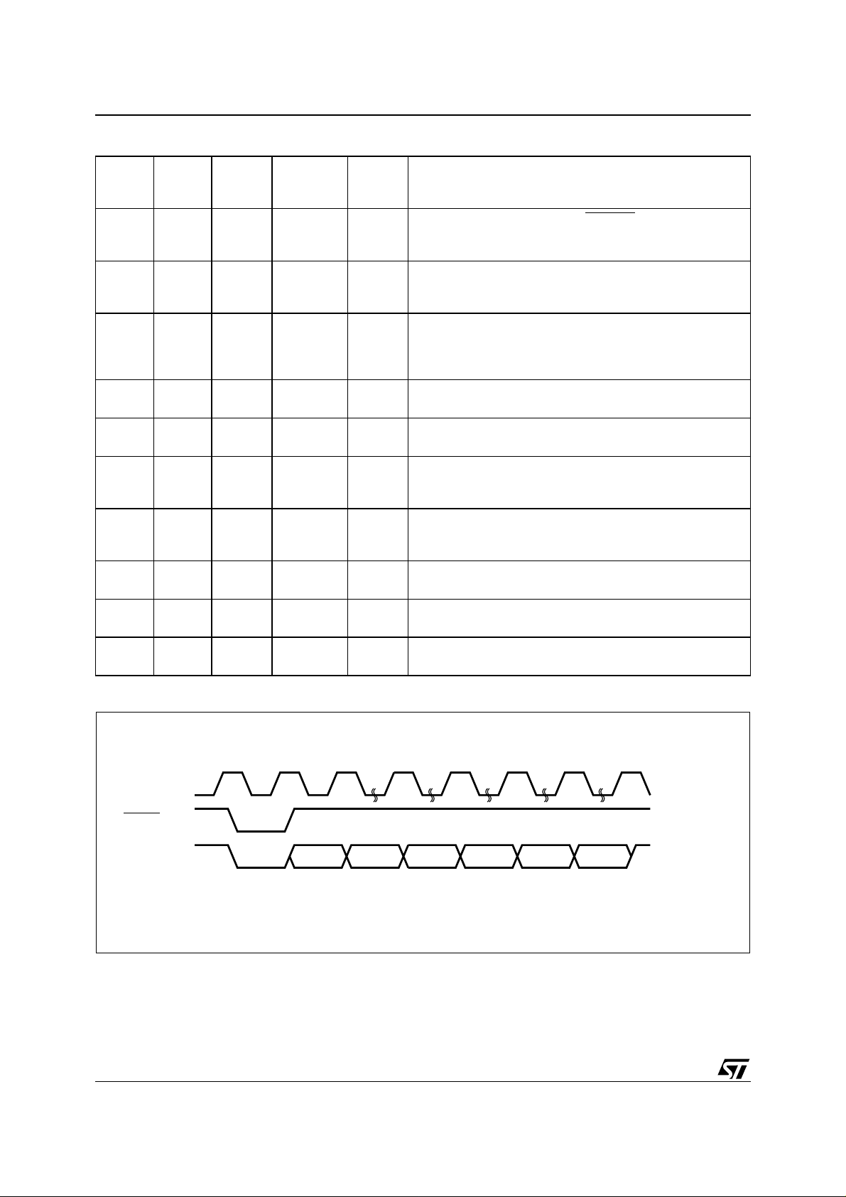
Figure 5. Bus Read Waveforms (LP C Interface)
CLK
LFRAME
CYCTYPE
+ DIR
1182322
ADDR TAR SYNC DATA TAR
10/39
LAD0-LAD3
Number of
clock cycles
START
AI04429
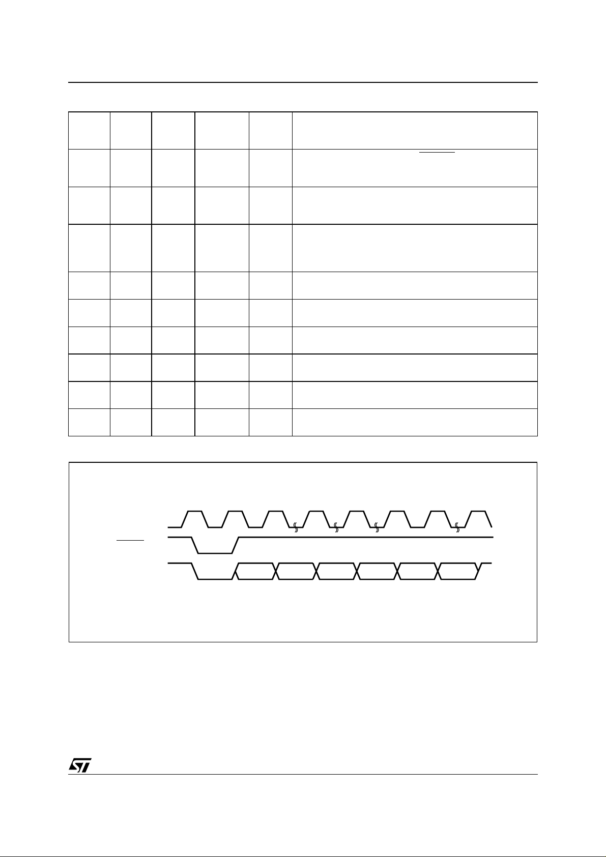
Table 6. Bus Write Field Definitions (LPC Interface)
Clock
Cycle
Number
Clock
Cycle
Count
Field
LAD0-
LAD3
Memory
I/O
M50LPW002
Description
1 1 START 0000b I
CYCTY
21
PE +
011Xb I
DIR
3-10 8 ADDR XXXX I
11-12 2 DATA XXXX I
13 1 TAR 1111b I
14 1 TAR
1111b
(float)
15 1 SYNC 0000b O
16 1 TAR 1111b O
17 1 TAR
1111b
(float)
N/A
On the rising edge of CLK with LFRAME
Low, the contents
of LAD0-LAD3 must be 0000b to indicate the start of a LPC
cycle.
Indicates the type of cycle. Bits 3:2 must be 01b. Bit 1
indicates the direction of transfer: 1b for write. Bit 0 is don’t
care (X).
A 32-bit address phase is transferred starting with the most
significant nibble first. A23-A31 must be set to 1. A22 = 1 for
Array, A22 = 0 for registers access. For A18-A21 values,
refer to Table 3.
Data transfer is two cycles, starting with the least significant
nibble.
The host drives LAD0-LAD3 to 1111b to indicate a
turnaround cycle.
The LPC Flash Memory takes control of LAD0-LAD3 during
O
this cycle.
The LPC Flash Memory drives LAD0-LAD3 to 0000b,
indicating it has received data or a command.
The LPC Flash Memory drives LAD0-LAD3 to 1111b,
indicating a turnaround cycle.
The LPC Flash Memory floats its outputs and the host takes
control of LAD0-LAD3.
Figure 6. Bus Write Waveforms (LPC Interface)
CLK
LFRAME
LAD0-LAD3
Number of
clock cycles
START
CYCTYPE
+ DIR
1182212
ADDR DATA TAR SYNC TAR
AI04430
11/39
M50LPW002
Address/Address Multiplexed (A/A Mux) Bus
Operations
The Address/Address Multiplexed (A/A Mux)
Interface has a more traditional style interface.
The signals consist of a multiplexed address
signals (A0-A10), data signals, (DQ0-DQ7) and
three control signals (RC
signal, RP
, can be used to reset the memory.
, G, W). An additional
The Address/Address Multiplexed (A/A Mux)
Interface is included for use by Flash
Programming equipment for faster factory
programming. Only a subset of the features
available to the Low Pin Count (LPC) Interface are
available; these include all the Commands but
exclude the Security features and other registers.
The following operations can be performed using
the appropriate bus cycles: Bus Read, Bus Write,
Output Disable and Reset.
When the Address/Address Multiplexed (A/A Mux)
Interface is selected all the blocks are
unprotected. It is not possible to protect any blocks
through this interface.
Bus Read. Bus Read operations are used to
output the contents of the Memory Array, the
Electronic Signature and the Status Register. A
valid Bus Read operation begins by latching the
Row Address and Column Address signals into
the memory using the Address Inputs, A0-A10,
and the Row/Column Address Select RC
Write Enable (W
be High, V
) and Interface Reset (RP) must
, and Output Enable, G, Low, VIL, in
IH
. Then
order to perform a Bus Read operation. The Data
Inputs/Outputs will output the value, see Figure
12, Read AC Waveforms (A/A Mux Interface), and
Table 25, Read AC Characteristics (A/A Mux
Interface), for details of when the output becomes
valid.
Bus Write. Bus Write operations write to the
Command Interface. A valid Bus Write operation
begins by latching the Row Address and Column
Address signals into the memory using the
Address Inputs, A0-A10, and the Row/Column
Address Select RC
the Data Inputs/Outputs; Output Enable, G
Interface Reset, RP
Enable, W
, must be Low, VIL. The Data Inputs/
. The data should be set up on
, and
, must be High, VIH and Write
Outputs are latched on the rising edge of Write
Enable, W
. See Figure 1 3, Write AC Waveforms
(A/A Mux Interface), and Table 26, Write AC
Characteristics (A/A Mux Interface), for details of
the timing requirements.
Output Disa bl e . The data outputs are high-impedance when the Output Enable, G
, is at VIH.
Reset. During Reset mode all internal circuits are
switched off, the memory is deselected and the
outputs are put in high-impedance. The memory is
in Reset mode when RP
held Low, V
for t
IL
is Low, VIL. RP must be
. If RP is goes Low, VIL,
PLPH
during a Program or Erase operation, the
operation is aborted and the memory cells affected
no longer contain valid data; the memory can take
up to t
to abort a Program or Erase operation.
PLRH
Table 7. A/A Mux Bus Operations
Operation G W RP
Bus Read
Bus Write
Output Disable
Reset
V
IL
V
IH
V
IH
V
or V
IL
IH
V
IH
V
IL
V
IH
VIL or V
Table 8. Manufacturer and Device Codes
Operation G
Manufacturer Code
Device Code
V
IL
V
IL
W RP A17-A1 A0 DQ7-DQ0
V
IH
V
IH
V
PP
V
IH
V
IH
V
IH
IH
V
IL
V
IH
V
IH
Don’t Care Data Output
VCC or V
Don’t Care Hi-Z
Don’t Care Hi-Z
V
V
PPH
IL
IL
V
IL
V
IH
DQ7-DQ0
Data Input
20h
31h
12/39
 Loading...