

SGS Thomson Microelectronics M48Z512AY-85PM1, M48Z512A-85PM1, M48Z512AY-70PM1, M48Z512AY, M48Z512A-70PM1 Datasheet
...
4 Mbit (512Kb x8) ZEROPOWERSRAM
■ INTEGRATED LOW POWER SRAM,
POWER-FAIL CONTROL CIRCUIT and
BATTERY
■ CONVENTIONAL SRAM OPERATION;
UNLIMITED WRITE CYCLES
■ 10 YEARS of DATA RETENTION in the
ABSENCE of POWER
■ AUTOMATIC POWER-FAIL CHIP DESELECT
and WRITE PROTECTION
■ WRITE PROTECT VOLTAGES
(V
= Power-fail Deselect Voltage):
PFD
– M48Z512A: 4.50V ≤ V
– M48Z512AY: 4.20V ≤ V
■ BATTERY INTERNALLY ISOLATED UNTIL
POWER IS APPLIED
■ PIN and FUNCTION COMPATIBLE with
JEDEC STANDARD 512K x 8 SRAMs
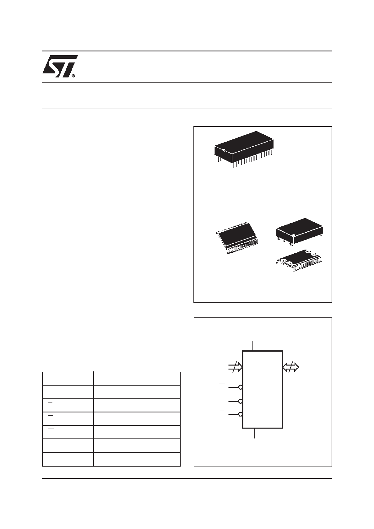
■ SURFACE MOUNT CHIP SET PACKAGING
INCLUDES a 28-PIN SOIC and a 32-LEAD
TSOP (SNAPHAT TOP TO BE ORDERED
SEPARATELY)
■ SOIC PACKAGE PROVIDES DIRECT
CONNECTION for a SNAPHAT TOP WHICH
CONTAINS the BATTERY
■ SNAPHAT
HOUSING (BATTERY) IS
REPLACEABLE
PFD
PFD
≤ 4.75V
≤ 4.50V
32
1
PMDIP32 (PM)
Module
32
1
TSOP II 32
(10 x 20mm)
Surface Mount Chip Set Solution (CS)
Figure 1. Logic Diagram
V
CC
M48Z512A
M48Z512AY
SNAPHAT (SH)
Battery
SOH28
Table 1. Signal Names
A0-A18 Address Inputs
DQ0-DQ7 Data Inputs / Outputs
E Chip Enable
G Output Enable
W Write Enable
V
CC
V
SS
Supply Voltage
Ground
A0-A18
W
19
M48Z512A
M48Z512AY
E
G
V
SS
8
DQ0-DQ7
AI02043
1/17March 2000
M48Z512A, M48Z512AY
Table 2. Absolute Maximum Ratings
Symbol Parameter Value Unit
T
A
T
STG
T
BIAS
(2)
T
SLD
V
IO
V
CC
Note: 1. Stresses greater thanthose listed under ”Absolute MaximumRatings” maycause permanent damage to the device. This is astress
rating only and functional operation of the device at these or any other conditions above those indicated in the operational section
of this specification is not implied. Exposure to the absolute maximum rating conditions for extended periods of time may affect
reliability.
2. Soldering temperature not to exceed 260°C for 10 seconds (total thermal budget not to exceed 150°C for longer than 30 seconds).
CAUTION: Negative undershoots below –0.3V are not allowed on any pin while in the Battery Back-up mode.
Ambient Operating Temperature 0 to 70 °C
Storage Temperature (VCCOff) –40 to 70 °C
Temperature Under Bias –40 to 70 °C
Lead Solder Temperature for 10 seconds 260 °C
Input or Output Voltages –0.3 to 7 V
Supply Voltage –0.3 to 7 V
(1)
Table 3. Operating Modes
Mode
Deselect
Write V
Read
Read V
V
CC
4.75V to 5.5V
or
4.5V to 5.5V
E G W DQ0-DQ7 Power
V
IH
IL
V
IL
IL
X X High Z Standby
XVILD
V
IL
V
IH
V
IH
V
IH
IN
D
OUT
High Z Active
Active
Active
Deselect
Deselect ≤ V
Note: 1. X = VIHor VIL;VSO= Battery Back-up Switchover Voltage.
to V
V
SO
PFD
SO
(min)
X X X High Z CMOS Standby
X X X High Z Battery Back-up Mode
Figure 2. DIP Connections
A18 V
A16
A14
A12
A7
A6
A5
A4
A3
A2
A1
A0
DQ0
DQ2
SS
1
2
4
5
6
7
M48Z512A
8
M48Z512AY
9
10
11
12
13
14
15
16
32
31
30
29
28
27
26
25
24
23
22
21
20
19
18
17
AI02044
CC
A15
A173
W
A13
A8
A9
A11
G
A10
E
DQ7
DQ6
DQ5DQ1
DQ4
DQ3V
DESCRIPTION
The M48Z512A/512AY ZEROPOWERRAM is a
non-volatile 4,194,304 bit Static RAM organized
as 524,288 words by 8 bits. The device combines
an internal lithium battery, a CMOS SRAM and a
control circuit in a plastic 32 pin DIP Module.
For surface mount environments ST provides a
Chip Set solution consisting of a 28 pin 330mil
SOIC NVRAM Supervisor (M40Z300) and a 32 pin
TSOP Type II (10 x 20mm) LPSRAM (M68Z512)
packages.
The unique design allows the SNAPHAT battery
package to be mounted on top of the SOIC package after the completion of the surface mount process. Insertion of the SNAPHAT housing after
reflow prevents potential battery damage due to
the high temperatures required for device surfacemounting. The SNAPHAT housing is keyed toprevent reverse insertion.
The SNAPHAT battery package is shipped separately in plastic anti-static tubes or in Tape & Reel
form. The part number is ”M4Zxx-BR00SH1”.
2/17
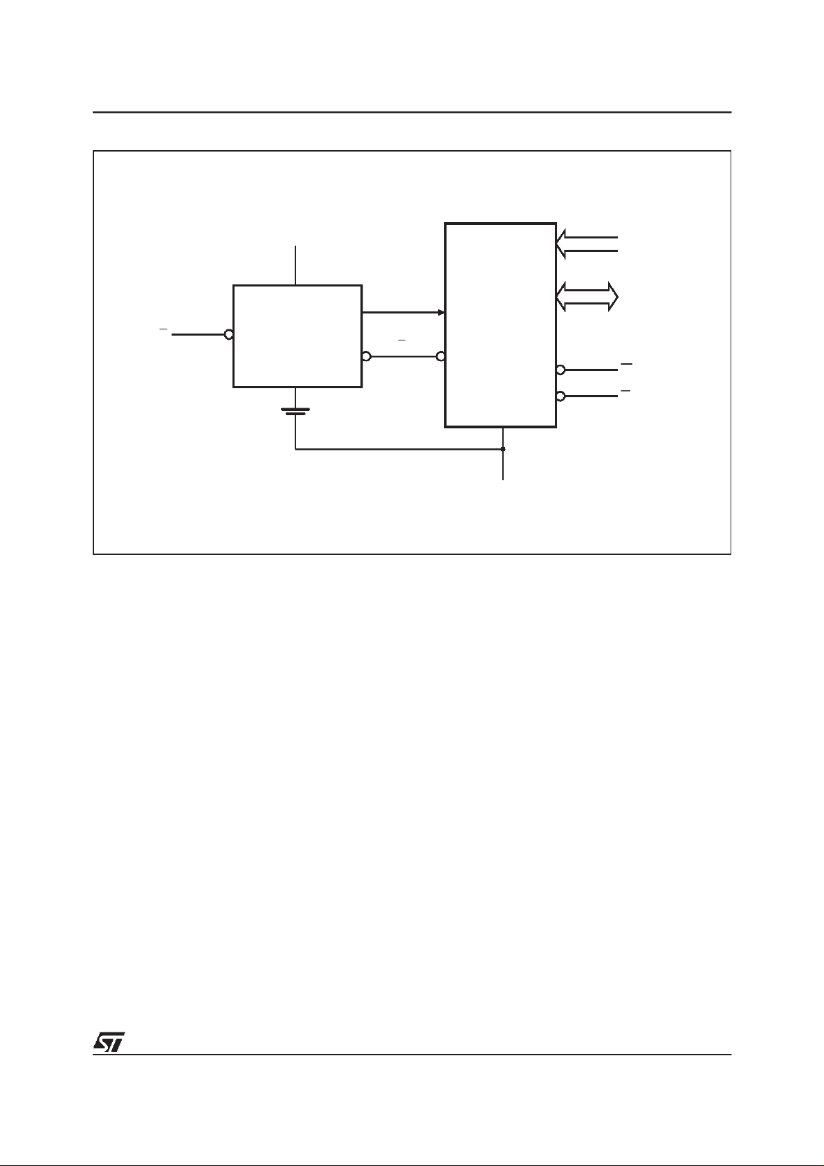
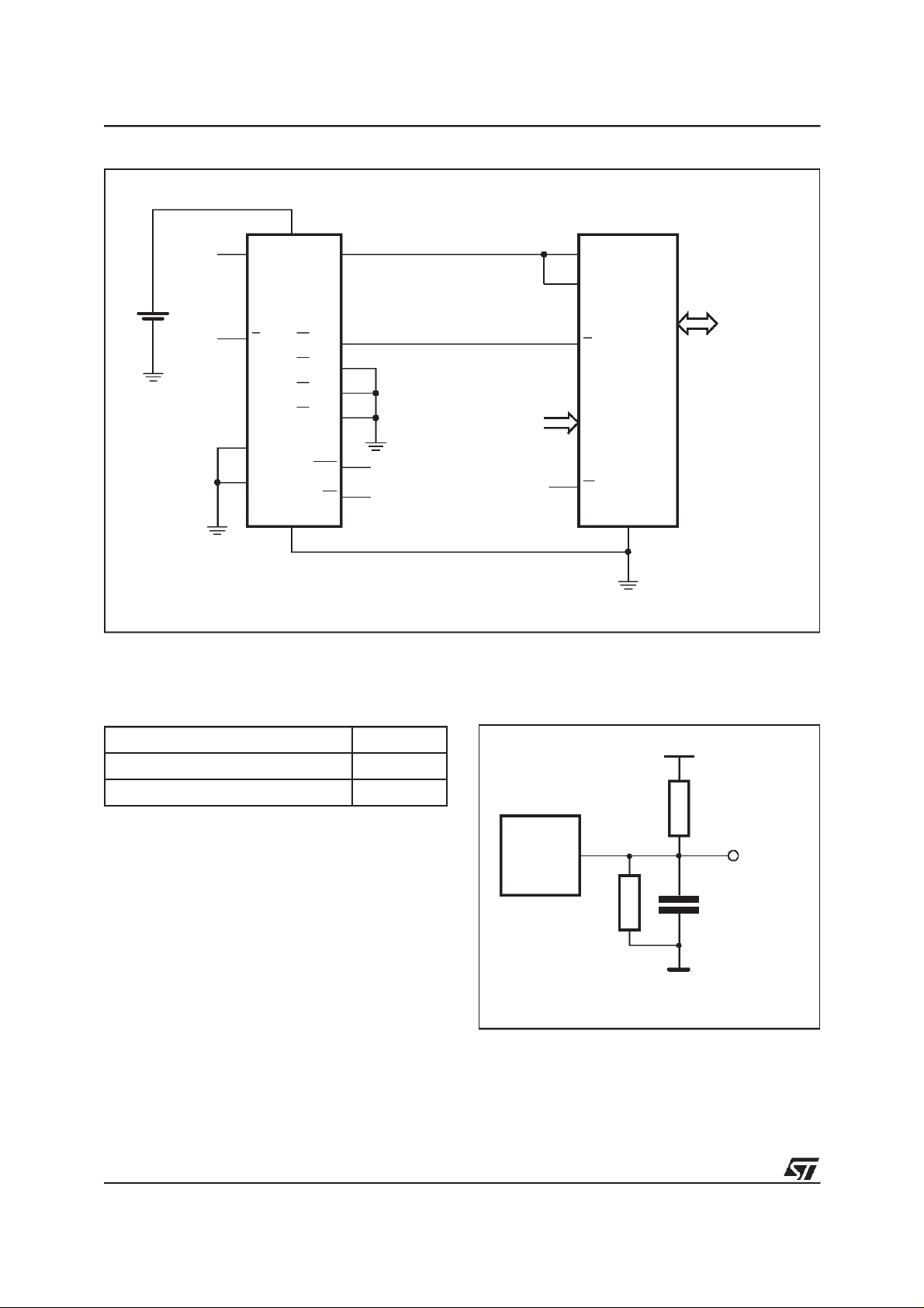
Figure 3. Block Diagram
M48Z512A, M48Z512AY
V
CC
A0-A18
POWER
VOLTAGE SENSE
E
AND
SWITCHING
CIRCUITRY
INTERNAL
BATTERY
The M48Z512A/512AY also has itsown Power-fail
Detect circuit.The controlcircuitry constantlymonitors the single 5V supply for an out of tolerance
condition. When VCCis out oftolerance, the circuit
write protects the SRAM, providing a high degree
of data security in the midst of unpredictable system operation brought on by low VCC.AsVCCfalls
below approximately 3V, the control circuitry connects the battery which maintains data until valid
power returns.
The ZEROPOWER RAM replaces industry standard SRAMs. It provides the nonvolatility of
PROMs without any requirement for special write
512K x
SRAM ARRAY
E
8
V
SS
DQ0-DQ7
W
G
AI02045
timing or limitations on the number of writes that
can be performed.
The M48Z512A/512AY has its own Power-fail Detect Circuit. The control circuitry constantly monitors the single 5V supply for an out of tolerance
condition. When VCCis out of tolerance, the circuit
write protects the SRAM, providing a high degree
of data security in the midst of unpredictable system operations brought on by low VCC.AsV
falls below approximately 3V, the control circuitry
connectsthe battery whichsustains data untilvalid
power returns.
CC
3/17
M48Z512A, M48Z512AY
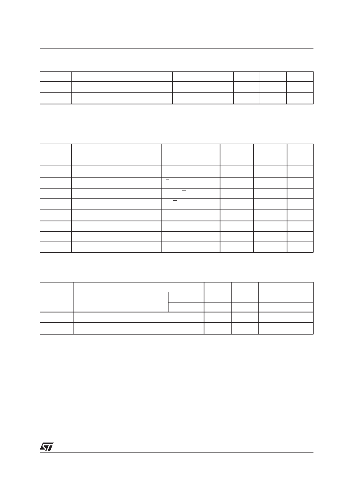
Figure 4. Hardware Hookup for SMT Chip Set
(2)
M40Z300
E1
E2
E3
E4
V
SS
V
CON
CON
CON
CON
OUT
RST
BL
SNAPHAT
BATTERY
THS
(3)
E
A
B
(1)
V
CC
E2
M68Z512
E
A0-A18
W
DQ0-DQ7
V
SS
AI03631
Note: 1. For pin connections, see individual data sheets for M40Z300 and M68Z512 at www.st.com.
2. Connect THS pin to V
3. SNAPHAT top ordered separately.
Table 4. AC Measurement Conditions
OUT
if 4.2V ≤ V
≤ 4.5V (M48Z512AY) or connect THS pin to VSSif 4.5V ≤ V
PFD
Figure 5. AC Testing Load Circuit
Input Rise and Fall Times ≤ 5ns
Input Pulse Voltages 0 to 3V
Input and Output Timing Ref. Voltages 1.5V
Note that Output Hi-Z is defined as the point where dataisno longer
driven.
DEVICE
UNDER
TEST
1kΩ
CLincludes JIG capacitance
≤ 4.75V (M48Z512A).
PFD
5V
1.9kΩ
CL= 100pF or
OUT
5pF
AI01030
4/17
M48Z512A, M48Z512AY
Table 5. Capacitance
(1, 2)
(TA=25°C, f = 1MHz)
Symbol Parameter Test Condition Min Max Unit
C
IN
C
IO
Note: 1. Effective capacitance measured with power supply at 5V.
2. Sampled only, not 100% tested.
3. Outputs deselected.
Input Capacitance
(3)
Input / Output Capacitance
V
V
OUT
IN
=0V
=0V
10 pF
10 pF
Table 6. DC Characteristics
(TA= 0 to 70 °C; VCC= 4.75V to 5.5V or 4.5V to 5.5V)
Symbol Parameter Test Condition Min Max Unit
(1)
I
LI
I
LO
I
CC
I
CC1
I
CC2
V
IL
V
IH
V
OL
V
OH
Note: 1. Outputs deselected.
Input Leakage Current
(1)
Output Leakage Current
Supply Current E = VIL, Outputs open 115 mA
Supply Current (Standby) TTL
Supply Current (Standby) CMOS
Input Low Voltage –0.3 0.8 V
Input High Voltage 2.2 VCC+ 0.3 V
Output Low Voltage
Output High Voltage IOH= –1mA 2.4 V
0V ≤ V
0V ≤ V
E ≥ V
I
OL
IN
OUT
E=V
– 0.2V
CC
= 2.1mA
≤ V
≤ V
IH
CC
CC
±1 µA
±1 µA
10 mA
5mA
0.4 V
Table 7. Power Down/Up TripPoints DC Characteristics
(1)
(TA= 0 to 70 °C)
Symbol Parameter Min Typ Max Unit
V
PFD
V
SO
t
DR
Note: 1. All voltages referenced to VSS.
2. At 25 °C.
Power-fail Deselect Voltage
Battery Back-up Switchover Voltage 3 V
(2)
Data Retention Time 10 YEARS
M48Z512A 4.5 4.6 4.75 V
M48Z512AY 4.2 4.3 4.5 V
5/17
M48Z512A, M48Z512AY
Table 8. Power Down/Up AC Characteristics
(TA= 0 to 70 °C)
Symbol Parameter Min Max Unit
(1)
t
F
t
FB
t
WP
t
R
V
(max) to V
(2)
PFD
V
(min) to VSOVCCFallTime
PFD
PFD
Write Protect Time from VCC=V
VSOto V
(max) VCCRise Time
PFD
(min) VCCFall Time
PFD
300 µs
10 µs
40 150 µs
0 µs
t
ER
Note: 1. V
2. V
E Recovery Time 40 120 ms
(max) to V
PFD
(min).
es V
PFD
(min) to VSOfall time of less than tFBmay cause corruption of RAM data.
PFD
(min) fall time of less than tFmay result indeselection/write protection not occurring until 200µs after VCCpass-
PFD
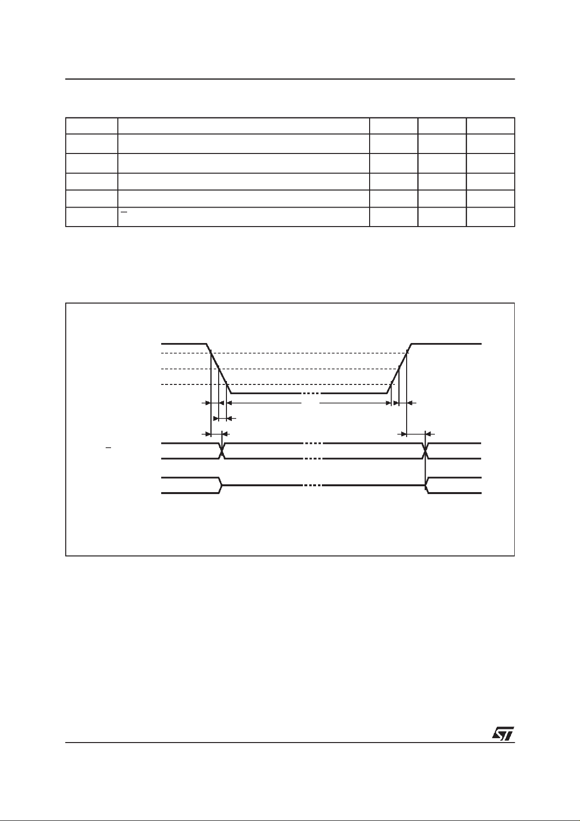
Figure 6. Power Down/Up Mode AC Waveforms
V
CC
V
(max)
PFD
V
(min)
PFD
V
SO
tF
tFB
tWP
E
OUTPUTS
VALID VALID
(PER CONTROL INPUT)
tDR
DON’T CARE
HIGH-Z
tR
tER
RECOGNIZEDRECOGNIZED
(PER CONTROL INPUT)
6/17
AI01031
 Loading...