

3.3V, 256 Kbit (32 Kbit x 8) ZEROPOWER® SRAM
FEATURES SUMMARY
■ INTEGRATED, ULTRA LOW POWER SRAM,
and POWER-FAIL CONTROL CIRCUIT
■ READ CYCLE TIME EQUALS WRITE CYCLE
TIME
■ AUTOMATIC POWER-FAIL CHIP DESELECT
and WRITE PROTECTION
■ WRITE PROTECT VOLTAGES:
= Power-fail Deselect Voltage)
(V
PFD
– M48Z32V: 2.7V ≤ V
■ ULTRA-LOW STANDBY CURRENT
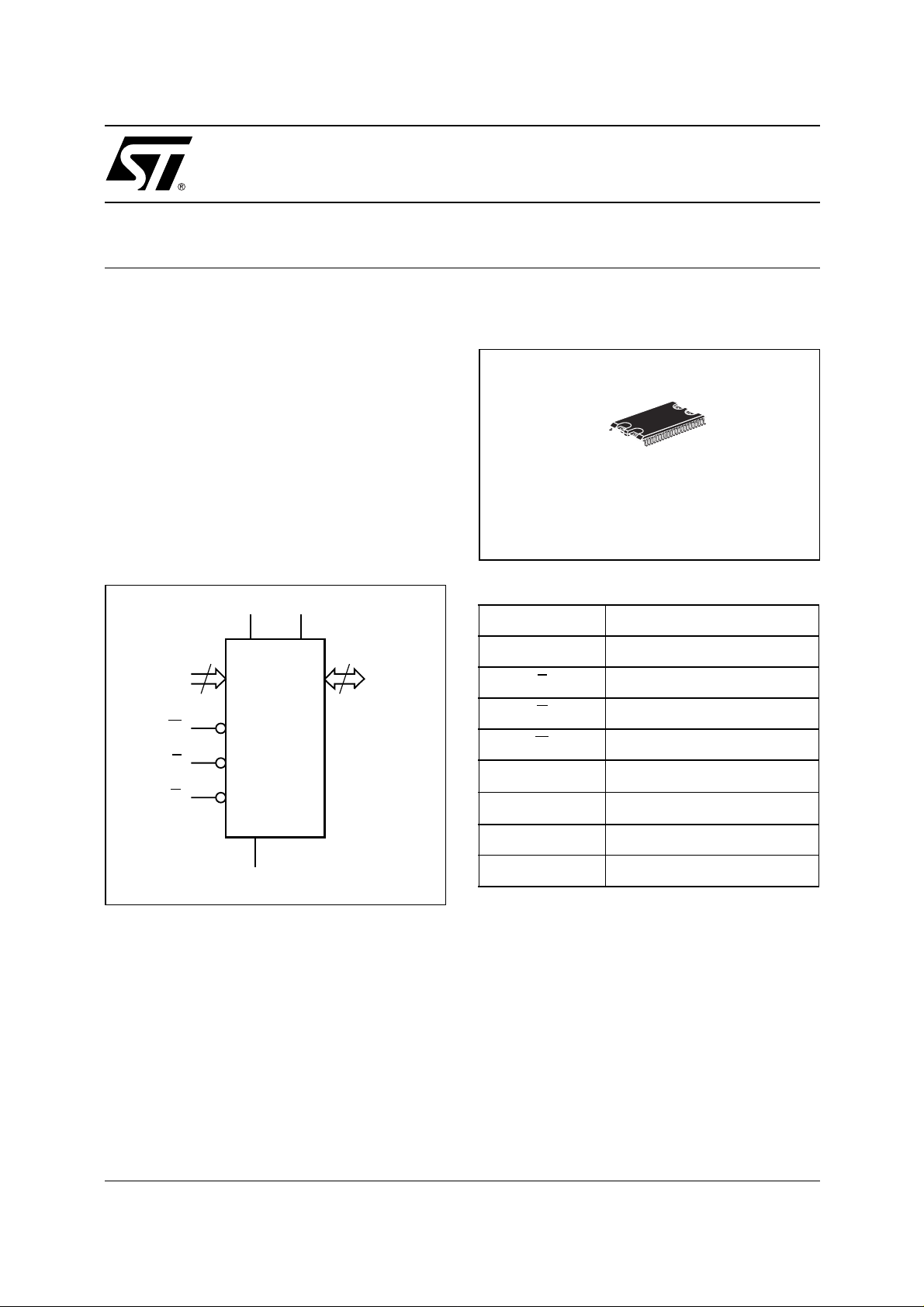
Figure 1. Logic Diagram
V
CC
PFD
≤ 3.0V
B +
M48Z32V
Figure 2. 44-pin, Hatless SOIC Package
44
1
SOH44 (MT)
Table 1. Signal Names
A0-A14 Address Inputs
A0-A14
W
15
M48Z32V
E
G
V
SS
8
DQ0-DQ7
AI04787
DQ0-DQ7 Data Inputs / Outputs
E
G
W
V
CC
V
SS
B + Positive Battery Pin
NC Not Connected
Chip Enable Input
Output Enable Input
WRITE Enable Input
Supply Voltage
Ground
1/16November 2002

M48Z32V
TABLE OF CONTENTS
DESCRIPTION . . . . . . . . . . . . . . . . . . . . . . . . . . . . . . . . . . . . . . . . . . . . . . . . . . . . . . . . . . . . . . . . . . . . 3
SOIC Connections (Figure 3.) . . . . . . . . . . . . . . . . . . . . . . . . . . . . . . . . . . . . . . . . . . . . . . . . . . . . . . 3
Block Diagram (Fi g ure 4 .) . . . . . . . . . . . . . . . . . . . . . . . . . . . . . . . . . . . . . . . . . . . . . . . . . . . . . . . . . 4
MAXIMUM RATING. . . . . . . . . . . . . . . . . . . . . . . . . . . . . . . . . . . . . . . . . . . . . . . . . . . . . . . . . . . . . . . . . 4
Absolute Maximum Rati ng s (Table 2.) . . . . . . . . . . . . . . . . . . . . . . . . . . . . . . . . . . . . . . . . . . . . . . .4
DC AND AC PARAMETERS. . . . . . . . . . . . . . . . . . . . . . . . . . . . . . . . . . . . . . . . . . . . . . . . . . . . . . . . . . 5
Operating and AC Measurement Conditions (Table 3.) . . . . . . . . . . . . . . . . . . . . . . . . . . . . . . . . . . 5
AC Measurement Load Circuit (Figure 5.). . . . . . . . . . . . . . . . . . . . . . . . . . . . . . . . . . . . . . . . . . . . .5
Capacitance (Table 4.) . . . . . . . . . . . . . . . . . . . . . . . . . . . . . . . . . . . . . . . . . . . . . . . . . . . . . . . . . . . 5
DC Characteristi cs (Table 5.) . . . . . . . . . . . . . . . . . . . . . . . . . . . . . . . . . . . . . . . . . . . . . . . . . . . . . . 6
OPERATING MODES . . . . . . . . . . . . . . . . . . . . . . . . . . . . . . . . . . . . . . . . . . . . . . . . . . . . . . . . . . . . . . . 6
Operating Modes (Table 6.) . . . . . . . . . . . . . . . . . . . . . . . . . . . . . . . . . . . . . . . . . . . . . . . . . . . . . . . . 6
READ Mode. . . . . . . . . . . . . . . . . . . . . . . . . . . . . . . . . . . . . . . . . . . . . . . . . . . . . . . . . . . . . . . . . . . . 7
READ Mode AC Waveforms (Figure 6.) . . . . . . . . . . . . . . . . . . . . . . . . . . . . . . . . . . . . . . . . . . . . . . 7
READ Mode AC Characteristic s (Table 7.) . . . . . . . . . . . . . . . . . . . . . . . . . . . . . . . . . . . . . . . . . . . . 8
WRITE Mode. . . . . . . . . . . . . . . . . . . . . . . . . . . . . . . . . . . . . . . . . . . . . . . . . . . . . . . . . . . . . . . . . . . 9
WRITE Enable Controlled, WRITE Mode AC Wav eforms (Figure 7.). . . . . . . . . . . . . . . . . . . . . . . .9
Chip Enable Controlled, WRITE Mode AC Waveforms (Figure 8.). . . . . . . . . . . . . . . . . . . . . . . . . . 9
WRITE Mode AC Characteristics (Table 8.) . . . . . . . . . . . . . . . . . . . . . . . . . . . . . . . . . . . . . . . . . . 10
Data Retention Mode. . . . . . . . . . . . . . . . . . . . . . . . . . . . . . . . . . . . . . . . . . . . . . . . . . . . . . . . . . . . 11
Power Down/Up Mode AC Waveforms (Figure 9.) . . . . . . . . . . . . . . . . . . . . . . . . . . . . . . . . . . . . . 11
Power Down/Up AC Characteristics (Table 9.) . . . . . . . . . . . . . . . . . . . . . . . . . . . . . . . . . . . . . . . . 11
Power Down/Up Trip Points DC Char ac te r i stics (Table 10.). . . . . . . . . . . . . . . . . . . . . . . . . . . . . . 12
V
Noise And Negative Going Transients. . . . . . . . . . . . . . . . . . . . . . . . . . . . . . . . . . . . . . . . . . .12
CC
Supply Voltage Protection (Figure 10.) . . . . . . . . . . . . . . . . . . . . . . . . . . . . . . . . . . . . . . . . . . . . . .1 2
PART NUMBERING . . . . . . . . . . . . . . . . . . . . . . . . . . . . . . . . . . . . . . . . . . . . . . . . . . . . . . . . . . . . . . . 13
PACKAGE MECHANICAL INFORMATION . . . . . . . . . . . . . . . . . . . . . . . . . . . . . . . . . . . . . . . . . . . . . 14
REVISION HISTORY . . . . . . . . . . . . . . . . . . . . . . . . . . . . . . . . . . . . . . . . . . . . . . . . . . . . . . . . . . . . . . . 15
2/16
M48Z32V
DESCRIPTION
®
The M48Z32V ZEROPOWER
RAM is a 32 Kbit x
8, non-volatile static RAM that integrates powerfail deselect circuitry and battery control logic on a
single die.
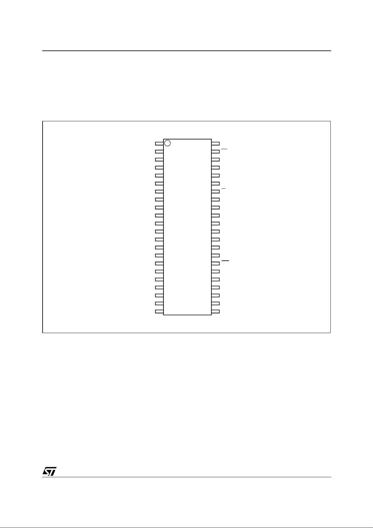
Figure 3. SOIC Connections
A14
A12
A7
A6
A5 A9
A4
NF
NC
NC
NC
NC
NC
NC
NC
A3
A2
A1
A0
DQ1
DQ2
V
SS
1
2
3
4
5
6
7
8
9
10
11
12
13
14
15
16
17
18
19
20
21
22
The 44-pin, 330mil SOIC provides a battery pin for
an external, user-supplied battery. T his is all that
is required to fully non-volatize the SRAM.
44
V
CC
43
W
42
A13
41
A8
40
39
A11
38
G
37
NC
36
NC
35
NC
34
M48Z32V
33
32
31
30
29
28
27
26
25
24
23
NC
NC
NC
NC
A10
CE
DQ7
DQ6
DQ5DQ0
DQ4
DQ3
B +
Note: NF, Pin 7 must be tied to VSS.
AI04786
3/16
M48Z32V
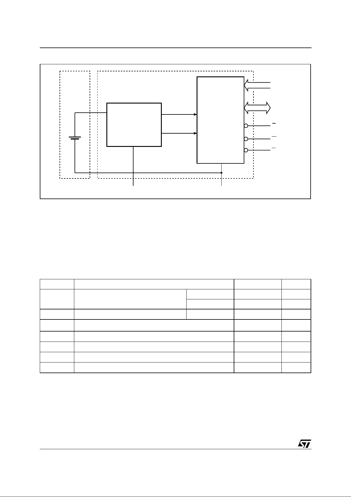
Figure 4. Block Diagram
A0-A14
LITHIUM
CELL
VOLTAGE SENSE
AND
SWITCHING
CIRCUITRY
USER
SUPPLIED
V
CC
MAXIMUM RATI N G
Stressing the device above the rating l isted in the
“Absolute Maximum Ratings” table may cause
permanent damage to the device. These are
stress ratings only and operation of the dev ice at
these or any other conditions above those indicated in the Operating sections of this specification is
POWER
V
PFD
32K x 8
SRAM ARRAY
V
SS
DQ0-DQ7
E
W
G
AI04788
not implied. Exposure to Absol ute Maxim um Rating conditions for extended periods may affect device reliability. Refer also to the
STMicroelectronics SURE Program and oth er relevant quality documents.
Table 2. Absolute Maximum Ratings
Symbol Parameter Value Unit
T
A
T
STG
T
SLD
V
IO
V
CC
I
O
P
D
Note: 1. Reflow at peak temperature of 215°C to 225°C for < 60 seconds (total thermal budget not to exceed 180°C for between 90 and 120
Ambient Operating Temperature
Storage Temperature (VCC Off, Oscillator Off)
(1)
Lead Solder Temperature for 10 seconds 260 °C
Input or Output Voltages
Supply Voltage –0.3 to 4.6 V
Output Current 20 mA
Power Dissipation 1 W
seconds).
CAUTION: Negative undershoots be l ow –0.3V are not allowed on a ny pin while i n th e Battery Ba ck -up mode.
Grade 1 0 to 70 °C
Grade 6 –40 to 85 °C
SOIC –55 to 125 °C
–0.3 to V
CC
+ 0.3
V
4/16
DC AND AC PARAMETERS
This section summarizes the operat ing and measurement conditions, as well as the DC and AC
characteristics of the device. The parameters in
the following DC and AC Characteristic tables are
derived from tests performed under the M easure-
Table 3. Operating and AC Measurement Conditions
(1)
Supply Voltage (V
CC
)
Ambient Operating Temperature (T
Parameter
)
A
M48Z32V
ment Conditions listed i n the relevant tables. Designers should check that the operating conditions
in their projects match the measurement conditions when using the quoted parameters.
M48Z32V Unit
3.0 to 3.6 V
Grade 1 0 to 70 °C
Grade 6 –40 to 85 °C
Load Capacitance (C
)
L
50
pF
Input Rise and Fall Times ≤ 5ns
Input Pulse Voltages 0 to 3 V
Input and Output Timing Ref. Voltages 1.5 V
Note: 1. Out put Hi-Z is de fined as the point where da ta is no l onger driven.
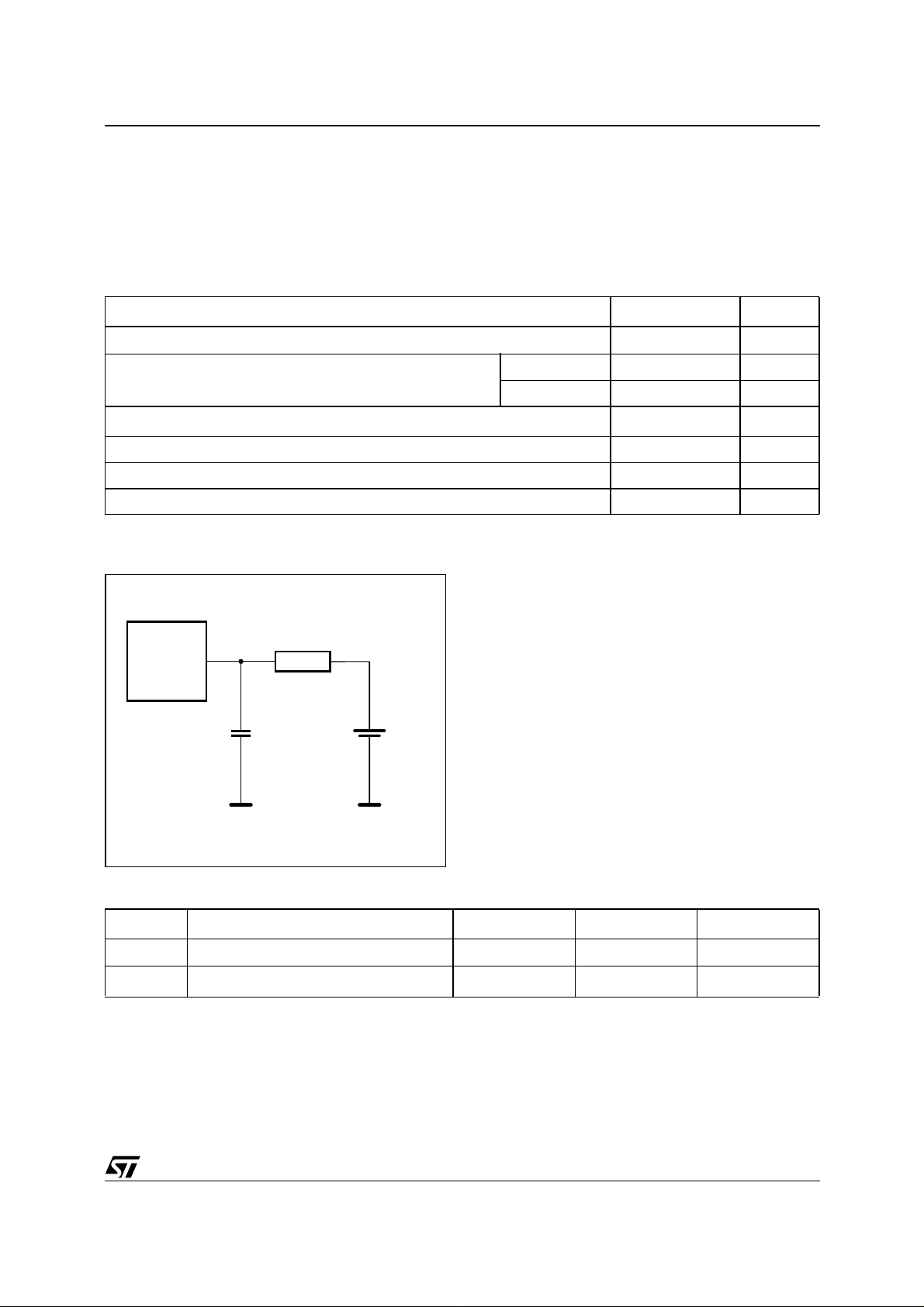
Figure 5. AC Me asureme nt Load Circui t
DEVICE
UNDER
TEST
CL includes JIG capacitance
645Ω
CL = 50pF or
5pF
1.75V
AI04789
Table 4. Capacitance
Symbol
C
IN
C
IO
Note: 1. Eff ective capa citance measured with power supply at 3.3V; sam pled only, not 100% test ed.
2. At 25°C, f = 1MHz.
3. Outputs desel ected.
Input Capacitance 10 pF
(3)
Input / Output Capacitance 10 pF
Parameter
(1,2)
Min Max Unit
5/16
 Loading...