

INTEGRATED LOW POWER SRAM,
POWER-FAILCONTROL CIRCUIT and
BATTERY
CONVENTIONAL SRAM OPERATION;
UNLIMITED WRITECYCLES
10 YEARSof DATA RETENTION in the
ABSENCEof POWER
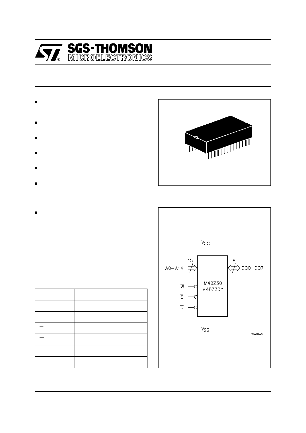
M48Z30
M48Z30Y
CMOS 32K x 8 ZEROPOWERSRAM
PIN and FUNCTION COMPATIBLEwith
JEDECSTANDARD 32K x 8SRAMs
AUTOMATIC POWER-FAILCHIP DESELECT
and WRITEPROTECTION
CHOICEof TWOWRITE PROTECT
VOLTAGES:
– M48Z30:4.5V ≤ V
– M48Z30Y:4.2V≤ V
PFD
PFD
≤ 4.75V
≤ 4.50V
BATTERYINTERNALLYISOLATEDUNTIL
POWERIS APPLIED
DESCRIPTION
The M48Z30/30Y32K x 8 ZEROPOWER
RAMis
a non-volatile262,144bitStaticRAMorganizedas
32,768 words by 8 bits. The device combines an
internallithium batteryand a full CMOSSRAMina
plastic 28 pin DIP Module. The ZEROPOWER
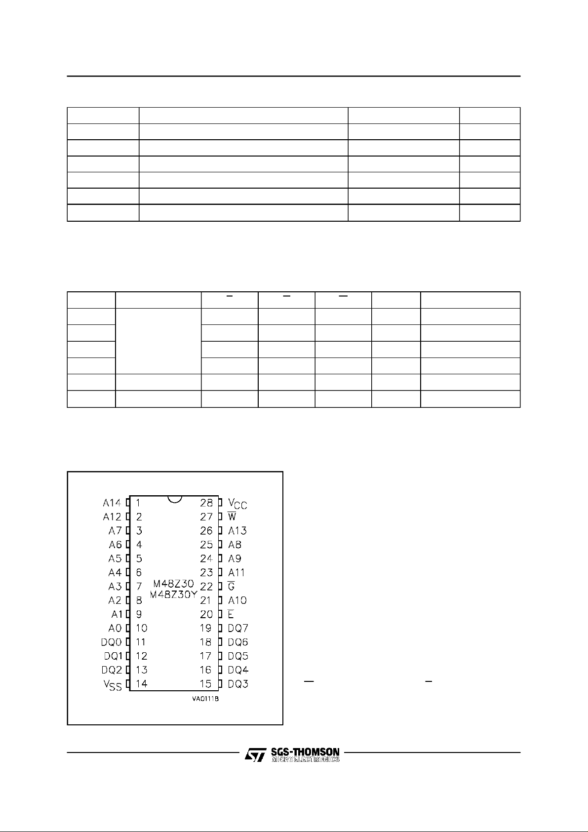
Table 1. Signal Names
A0 - A14 Address Inputs
28
1
PMDIP28 (PM)
Module
Figure 1. Logic Diagram
DQ0 - DQ7 Data Inputs / Outputs
E Chip Enable
G Output Enable
W Write Enable
V
CC
V
SS
July 1994 1/12
Supply Voltage
Ground
M48Z30, M48Z30Y
Table 2. Absolute MaximumRatings
Symbol Parameter Value Unit
T
A
T
STG
T
BIAS
T
SLD
V
IO
V
CC
Note: Stresses greater than those listed under ”Absolute Maximum Ratings” may cause permanent damage to the device. This is a stress
rating only and functional operation of the device at these or any other conditions above those indicated in the operational section of this
specification is not implied. Exposure to the absolute maximumratings conditions for extended periods of time may affect reliability.
CAUTION: Negative undershootsbelow –0.3 volts are notallowed onany pin while in the Battery Back-up mode.
Table 3. OperatingModes
Ambient Operating Temperature 0 to 70 °C
Storage Temperature(VCCOff) –40 to 70 °C
Temperature Under Bias –10 to 70 °C
Lead Soldering Temperature for 10 seconds 260 °C
Input or Output Voltages –0.3 to7 V
Supply Voltage –0.3 to7 V
Mode V
CC
Deselect
Write V
Read V
4.75V to 5.5V
or
4.5V to 5.5V
Read V
Deselect V
SO
Deselect ≤ V
Note:X=VIHor V
IL
to V
(min) X X X High Z CMOS Standby
PFD
SO
Figure2. DIP Pin Connections
E G W DQ0-DQ7 Power
V
IH
IL
IL
IL
X X High Z Standby
XVILD
V
IL
V
IH
V
IH
V
IH
IN
D
OUT
High Z Active
Active
Active
X X X High Z Battery Back-up Mode
DESCRIPTION (cont’d)
RAMdirectlyreplacesindustrystandardSRAMs.It
alsofits into manyEPROMandEEPROM sockets,
providing the nonvolatilityof PROMs without any
requirement for special write timing or limitations
on the number of writes that can be performed.
The M48Z30/30Y has its own Power-fail Detect
Circuit.Thecontrolcircuitryconstantlymonitorsthe
single5V supply for an out of tolerancecondition.
When V
is out of tolerance, the circuit write
CC
protectstheSRAM,providinga highdegreeofdata
security in the midst of unpredictable system operationsbrought onby lowV
.AsVCCfallsbelow
CC
approximately3V,the controlcircuitryconnectsthe
battery which sustains data until valid power returns.
2/12
READMODE
The M48Z30/30Y is in the Read Mode whenever
W(Write Enable)ishighandE(ChipEnable)islow.
The device architecture allows ripple-through accessof data from eight of 262,144locations in the
static storage array. Thus, the unique address
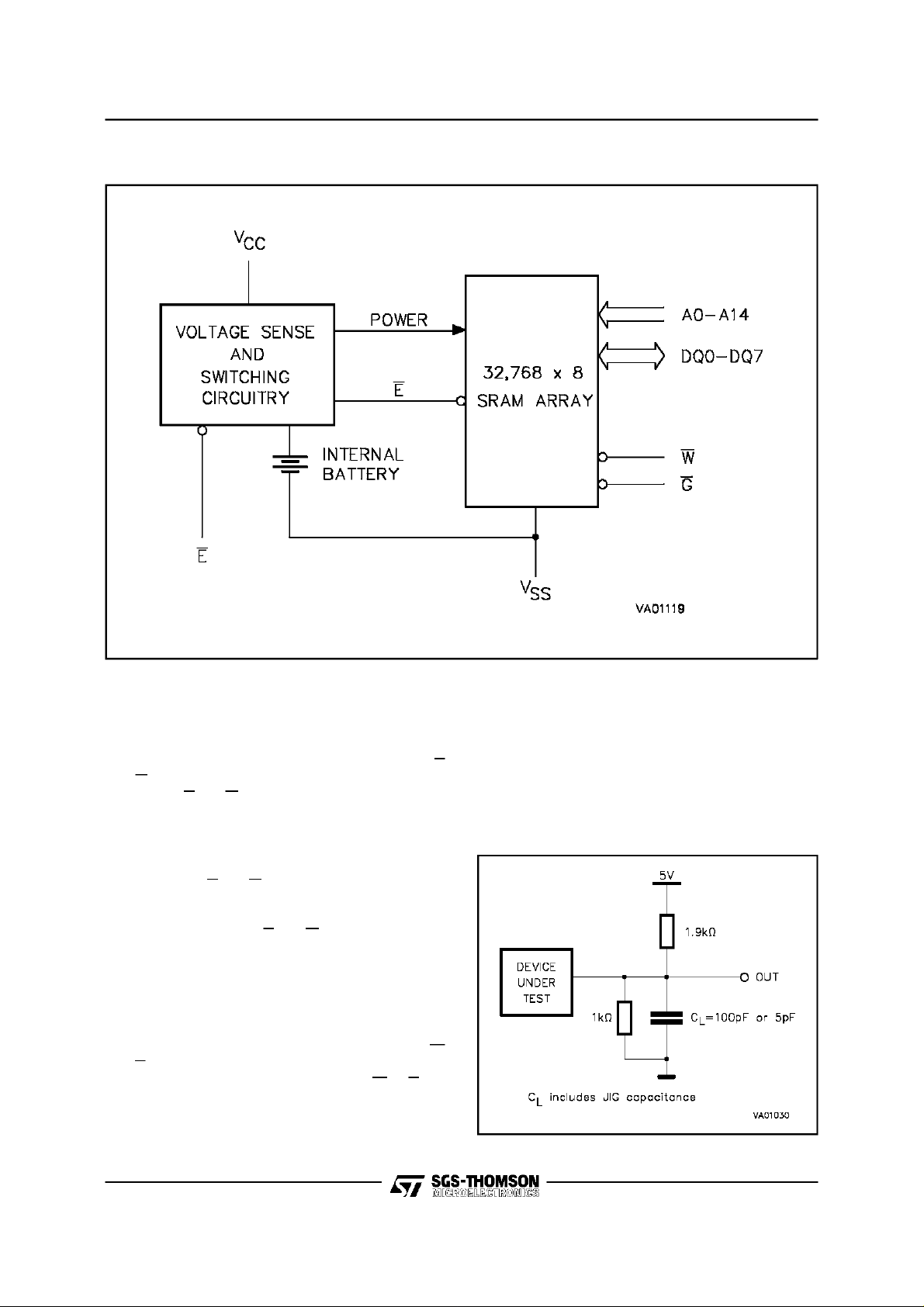
Figure3. Block Diagram
M48Z30, M48Z30Y
specified by the 15 Address Inputs defines which
one of the32,768 bytes of data is to be accessed.
Valid data will be available at the Data I/O pins
within t
(Address Access Time) after the last
AVQV
addressinput signal is stable, providing that theE
and G (OutputEnable) access times are alsosatisfied.If theE andGaccesstimesarenotmet, valid
data will be availableafter the later ofChipEnable
AccessTime(t
).
(t
GLQV
)orOutputEnableAccessTime
ELQV
The state of the eight three-stateData I/Osignals
iscontrolledbyEand G.Iftheoutputsareactivated
before t
indeterminate state until t
, the data lines will be driven to an
AVQV
. If the Address In-
AVQV
putsare changedwhile Eand Gremainlow, output
data will remain valid for t
(Output Data Hold
AXQX
Time) but will go indeterminate until the next AddressAccess.
WRITE MODE
TheM48Z30/30Yis inthe Write ModewheneverW
and E are active.The start of a write is referenced
fromthe latter occurring falling edge of W or E.
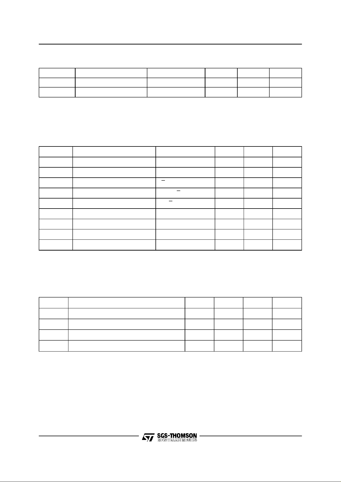
AC MEASUREMENT CONDITIONS
Input Rise and Fall Times ≤ 5ns
Input Pulse Voltages 0 to 3V
Input and Output Timing Ref. Voltages 1.5V
Note that Output Hi-Z is defined as the point where data
is no longer driven.
Figure 4. AC TestingLoad Circuit
3/12
M48Z30, M48Z30Y
Table4. Capacitance
(1, 2)
(TA=25°C, f = 1 MHz)
Symbol Parameter TestCondition Min Max Unit
C
IN
(3)
C
IO
Notes:1. Effective capacitance measured with power supply at 5V.
2. Sampled only,not 100% tested.
3. Outputs deselected
Input Capacitance VIN=0V 10 pF
Input / Output Capacitance V
=0V 10 pF
OUT
Table 5. DC Characteristics (TA= 0 to 70°C;VCC= 4.75V to 5.5Vor 4.5Vto 5.5V)
Symbol Parameter Test Condition Min Max Unit
(1)
I
LI
(1)
I
LO
I
CC
I
CC1
I
CC2
V
IL
V
IH
V
OL
V
OH
Note: 1. Outputs deselected.
Input Leakage Current 0V ≤ VIN≤ V
Output Leakage Current 0V ≤ V
OUT
≤ V
CC
CC
±1 µA
±1 µA
Supply Current E = VIL, Outputs open 85 mA
Supply Current (Standby) TTL E = V
IH
7mA
Supply Current (Standby) CMOS E≥ VCC– 0.2V 4 mA
Input Low Voltage –0.3 0.8 V
Input High Voltage 2.2 VCC+ 0.3 V
Output Low Voltage IOL= 2.1mA 0.4 V
Output High Voltage IOH= –1mA 2.4 V
Table6. Power Down/Up Trip Points DC Characteristics
(1)
(TA=0 to 70°C)
Symbol Parameter Min Typ Max Unit
V
PFD
V
PFD
V
SO
t
DR
Notes: 1. All voltages referenced to VSS.
2. @ 25°C
Power-fail Deselect Voltage(M48Z30) 4.5 4.6 4.75 V
Power-fail Deselect Voltage(M48Z30Y) 4.2 4.3 4.5 V
Battery Back-up Switchover Voltage 3 V
(2)
Data Retention Time 10 YEARS
4/12
 Loading...