

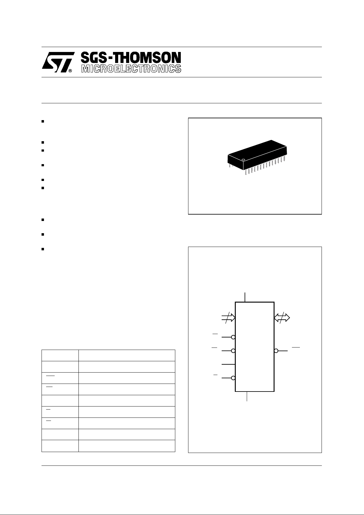
AI01184
13
A0-A12
W
DQ0-DQ7
V
CC
M48Z09
M48Z19
G
E2
V
SS
8
E1 INT
Figure 1. Logic Diagram
M48Z09
M48Z19
CMOS 8K x 8 ZEROPOWER SRAM
INTEGRATED ULTRA LOW POWER SRAM,
POWE R-FAIL CONTROL CIRCUI T and
BA TTERY
UNLIMITED WRI TE CYCLE S
READ CYCLE TIME EQUALS WRITE CYCLE
TIME
AUTOMA TIC POWER-F AIL CHIP DESELECT and
WRITE PROTECTION
POWER-FAIL INTERRUP T
CHOICE of TWO WRITE PROTECT
VOLTAGES:
– M48Z09: 4. 5V ≤ V
PFD
≤ 4.75V
– M48Z19: 4. 2V ≤ V
PFD
≤ 4.5V
SELF CONTAI NED B ATTER Y in the C AP HAT
DIP PACKAGE
11 YEARS of DAT A RETENTION in the
ABSENCE of POWER
PIN and FUNCTIO N CO MPATIBLE with the
MK48Z09, 19 and JEDE C STANDARD 8K x 8
SRAMs
DESCRIPT IO N
The M48Z09,19 ZERO POWER
®
RAM is an 8K x 8
non-volatile static RAM which is pin and function
compatible with the MK48Z09, 19.
A special 28 pin 600mil DIP CAPHAT package
houses the M48Z09,19 silicon with a long life lithium button cell to form a highly integrated battery
backed-up memory solut ion.
A0-A12 Address Inputs
DQ0-DQ7 Data Inputs / Outputs
INT Power Fail Interrupt
E1 Chip Enable 1
E2 Chip Enable 2
G Output Enable
W Write Enable
V
CC
Supply Voltage
V
SS
Ground
Table 1. Signal Names
28
1
PCDIP28 (PC)
Battery CAPHAT
November 1994 1/13
Symbol Parameter Value Unit
T
A
Ambient Operating Temperature 0 to 70
°C
T
STG
Storage Temperature (VCC Off) –40 to 85
°C
V
IO
Input or Output Voltages –0.3 to 7 V
V
CC
Supply Voltage –0.3 to 7 V
I
O
Output Current 20 mA
P
D
Power Dissipation 1 W
Note: Stresses greater than those listed under "Absolute Maximum Ratings" may cause permanent damage to the device. This is a stress
rating only and functional operation of the device at these or any other conditions above those indicated in the operational section of this
specification is not implied. Ex p osur e to the absolut e maximum rat ings conditi ons for extended periods of time may affect reliability.
CAUTION: Negative undershoots below –0.3 volts are not allowed on any pin while in the Battery Back-up mode.
Table 2. Absolut e Maxi mum Rat in gs
Mode V
CC
E1 E2 G W DQ0-DQ7 Power
Deselect
4.75V to 5.5V
or
4.5V to 5.5V
V
IH
X X X High Z Standby
Deselect X V
IL
X X High Z Standby
Write V
IL
V
IH
XVILD
IN
Active
Read V
IL
V
IH
V
IL
V
IH
D
OUT
Active
Read V
IL
V
IH
V
IH
V
IH
High Z Active
Deselect V
SO
to V
PFD
(min) X X X X High Z CMOS Standby
Deselect
≤ V
SO
X X X X High Z Battery Back-up Mode
Note: X = VIH or V
IL
Table 3. Operating Modes
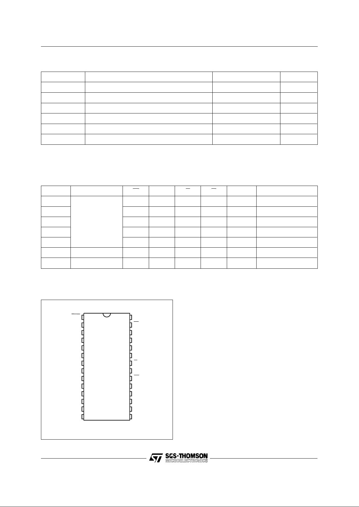
A1
A0
DQ0
A7
A4
A3
A2
A6
A5
E2
A10
A8
A9
DQ7
W
A11
G
E1
DQ5DQ1
DQ2
DQ3V
SS
DQ4
DQ6
A12
INT V
CC
AI01185
M48Z09
M49Z19
8
1
2
3
4
5
6
7
9
10
11
12
13
14
16
15
28
27
26
25
24
23
22
21
20
19
18
17
Figure 2A. DIP Pin Connections
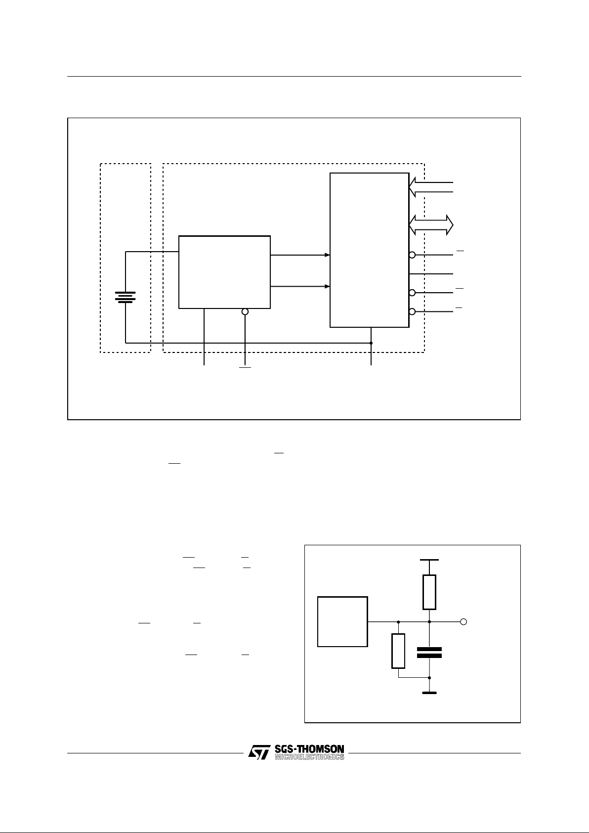
The M48Z09,19 button cell has sufficient capacity
and storage life to maintain data for an accumulated time period of at least 1 1 years in the absence
of power over the operating temp erature range.
The M48Z09,19 is a non-volatile pin and function
equivalent to any JEDEC standard 8K x 8 SRAM.
It also easily fits into many ROM, EPROM, and
EEPROM sockets, providing the non-volatility of
PROMs without any requirement for special write
timing or limitations on the number of writes that
can be performed.
The M48Z09,19 also has it s own Power-f ail Detect
circuit. The control circ uitry constantly monitor s the
single 5V supply for an out of tolerance condition.
When V
CC
is out of tolerance, the circuit write
protects the SRAM, providing a high degree of data
security in the midst of unpredict able system operation brought on by low V
CC
. As VCC falls below
approximately 3V, the cont rol circuitry connects the
battery which maintains data and clock operation
until valid power returns.
DESCRIPTI ON (cont ’d )
2/13
M48Z09, M4 8Z19
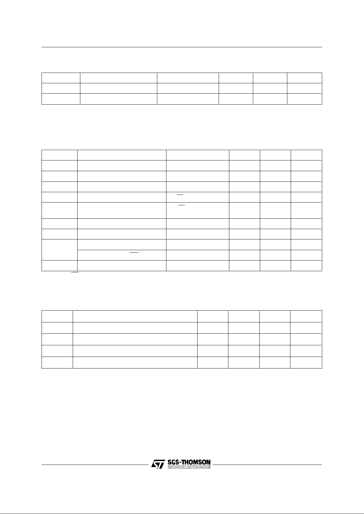
AI01398
5V
OUT
CL = 100pF or 30pF
CL includes JIG capacitance
1.8kΩ
DEVICE
UNDER
TEST
1kΩ
Figure 4. AC Test ing L o ad Circuit
Input Rise and Fall Times
≤ 5ns
Input Pulse Voltages 0 to 3V
Input and Output Timing Ref. Voltages 1.5V
AC MEASUREMEN T CONDI TIONS
Note that Output Hi-Z is defined as the point where data
is no longer driven.
AI01397
LITHIUM
CELL
V
PFD
V
CC
V
SS
VOLTAGE SENSE
AND
SWITCHING
CIRCUITRY
8K x 8
SRAM ARRAY
A0-A12
DQ0-DQ7
E1
W
G
POWER
E2
INT
Figure 3. Block Diagram
READ MODE
The M48Z09,19 is in the Read Mode whenever W
(Write Enable) is high,
E1 (Chip Enable 1) is low,
and E2 (Chip Enable 2) is high. The device architecture all ows ripple- through access of data from
eight of 65,536 locations in the static storage array .
Thus, the unique address specified by the 13 Address Inputs defines which one of the 8,192 bytes
of data is to be accessed. Valid data will be available at the Data I/O pins within t
AVQV
(Address
Access Time) after the last address input signal is
stable, providing that the
E1, E2, and G access
times are also satisf ied. If the
E1, E2 and G access
times are not met, valid data will be available after
the latter of the Chip Enable Acces s T im es (t
E1LQV
or t
E2HQV
) or Output Enable Access Time (t
GLQV
).
The state of the eight three-state Data I/O signals
is controlled by
E1, E2 and G. If the o utputs are
activated bef ore t
AVQV
, the data lines will be driven
to an indeterminate state unt il t
A VQV
. If the A ddress
Inputs are changed while
E1, E2 and G remain
active, output data will remain valid for t
AXQX
(Output Data Hold Time) but will go indeterminate until
the next A ddress A ccess.
3/13
M48Z09, M48Z19
Symbol Parameter Test Condition Min Max Unit
I
LI
Input Leakage Current
0V ≤ V
IN
≤ V
CC
±1 µA
I
LO
Output Leakage Current
0V ≤ V
OUT
≤ V
CC
±5 µA
I
CC
Supply Current Outputs open 80 mA
I
CC1
Supply Current (Standby) TTL E1 = VIH, E2 = V
IL
3mA
I
CC2
Supply Current (Standby) CMOS
E1 = VCC – 0.2V,
E2 = V
SS
+ 0.2V
3mA
V
IL
Input Low Voltage –0.3 0.8 V
V
IH
Input High Voltage 2.2 VCC + 0.3 V
V
OL
Output Low Voltage IOL = 2.1mA 0.4 V
Output Low Voltage (
INT)
(1)
IOL = 0.5mA 0.4 V
V
OH
Output High Voltage IOH = –1mA 2.4 V
Note: 1. The INT pin is Open Drain.
Table 5. DC Characteristics (TA = 0 to 70°C; VCC = 4.75V to 5.5V or 4.5V to 5.5V)
Symbol Parameter Test Condition Min Max Unit
C
IN
Input Capacitance VIN = 0V 10 pF
C
IO
(2)
Input / Output Capacitance V
OUT
= 0V 10 pF
Notes: 1. Effecti ve capacita nce calculated from th e equation C = I∆t/∆V with ∆V = 3V and power supply at 5V.
2. Outputs deselected
Table 4. Capacitance
(1)
(TA = 25 °C)
Symbol Parameter Min Typ Max Unit
V
PFD
Power-fail Deselect Voltage (M48Z09) 4.5 4.6 4.75 V
V
PFD
Power-fail Deselect Voltage (M48Z19) 4.2 4.3 4.5 V
V
SO
Battery Back-up Switchover Voltage 3.0 V
t
DR
Expected Data Retention Time 11 YEARS
Note: 1. All voltages referenced to VSS.
Table 6. Power Down/Up Trip Points DC Characteristics
(1)
(TA = 0 to 70°C)
4/13
M48Z09, M4 8Z19
 Loading...