

3.3V/5V 1 Mbit (128Kb x8) ZEROPOWER® SRAM
■ INTEGRATED ULTRA LOW POWER SRAM,
POWER-FAIL CONTROL CIRCUIT, and
BATTERY
■ AUTOMATIC POWER-FAIL CHIP DESELECT
AND WRITE PROTECTIO N
■ MICROPROCESSOR POWER-ON RESET
(RESET VALID EVEN DURING BATTERY
BACK-UP MODE)
■ BATTERY LOW PIN - PROVID ES WA RNI N G
OF BATTERY END-OF-LIFE
■ WRITE PROTECT VOLTAGES
= Power-fail Deselect Voltage):
(V
PFD
– M48Z129Y: 4.2V ≤ V
– M48Z129V: 2.7V ≤ V
■ CONVENTIONAL SRAM OPERATION;
UNLIMITED WRITE CYCLES
■ 10 YEARS OF DATA RETENTION IN THE
ABSENCE OF POWER
■ PIN AND FUNCTION COMPATIBLE WITH
JEDEC STANDARD 128Kb x 8 SRAMS
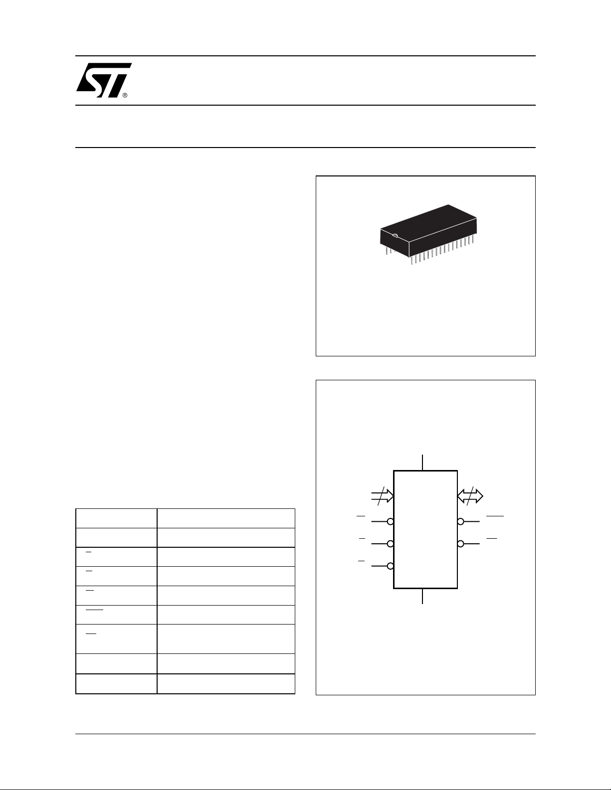
■ SELF CONTAINED BATTERY IN DIP
PACKAGE
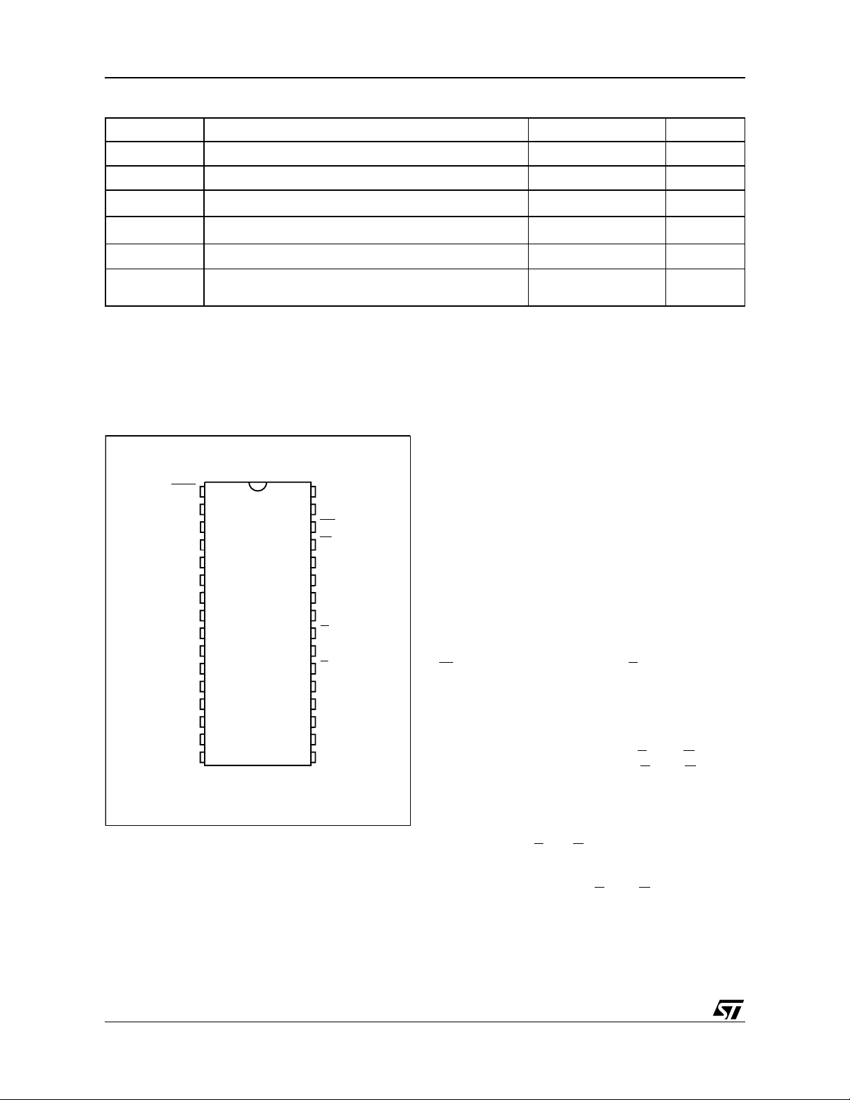
Table 1. Signal Names
A0-A16 Address Inputs
DQ0-DQ7 Data Inputs / Outputs
E
G
Chip Enable
Output Enable
PFD
PFD
≤ 4.5V
≤ 3.0V
M48Z129Y
M48Z129V
32
1
PMDIP32 (PM)
Module
Figure 1. Logic Diagram
V
CC
17
A0-A16 DQ0-DQ7
W RST
E
G
M48Z129Y
M48Z129V
8
BL
W
RST
BL
V
CC
V
SS
Write Enable
Reset Output (Open Drain)
Battery Low Output (Open
Drain)
Supply Voltage
Ground
V
SS
AI02309
1/13June 2000
M48Z129Y, M48Z129V
Table 2. Absolute Maximum Ratings
Symbol Parameter Value Unit
T
A
T
STG
T
BIAS
(2)
T
SLD
V
IO
V
CC
Note: 1. Stresses greater than those listed under "Absolute Maximum Ratings" may cause permanent damage to the device. This is a stress
rating only and functional opera tion of the dev i ce at these or any other conditions above thos e i ndi cated in th e operational section
of this spec ification is not im plied. Exposure t o the abso lute max imum rat ing cond itions for extende d period s of tim e may affe ct
reliability.
2. Soldering temperature not to exceed 260°C for 10 seconds (total thermal budget not to exceed 150°C for longer than 30 seconds).
CAUTION: Negative undershoots below –0. 3V are not allowed on any pin wh i l e i n the Batter y Back-up mod e.
Ambient Operating Temperature 0 to 70 °C
Storage Temperature (VCC Off)
Temperature Under Bias
Lead Solder Temperature for 10 seconds 260 °C
Input or Output Voltages
Supply Voltage M48Z129Y
Figure 2A. DIP Pin Connections
(1)
–40 to 70 °C
–10 to 70 °C
M48Z129V
–0.3 to V
–0.3 to 7.0
–0.3 to 4.6
CC
+0.3
V
V
128K x 8 SRAM. It also provides the non-volatility
of FLASH without any requirement for special
write timing or limitations on the number o f writes
that can be performed.
RST V
1
A16
2
3
A14
4
A12
5
A7
6
A6
7
A5
8
A4
A3
A2
A1
A0
DQ0
DQ2
SS
M48Z129Y
M48Z129V
9
10
11
12
13
14
15
16
32
31
30
29
28
27
26
25
24
23
22
21
20
19
18
17
AI02310
CC
A15
BL
W
A13
A8
A9
A11
G
A10
E
DQ7
DQ6
DQ5DQ1
DQ4
DQ3V
The M48Z129Y/V also has its own Power-Fail Detect circuit. This control circuitry constantly monitors the supply voltage for an out of tolerance
condition. When V
is out of tolerance, the circuit
CC
write protects the SRAM, providing data security in
the midst of unpredictable system operation. As
V
falls, the control circuit ry automatical ly switch-
CC
es to the battery, maintaining data until valid power
is restored.
READ MODE
The M48Z129Y/V is in the Read Mode whenever
(Write Enable) is high and E (Chip Enable) is
W
low. The unique addres s specified b y the 17 Address Inputs defines which one of the 131,072
bytes of data is to be accessed. Valid data will be
available at the Data I/O pins within t
AVQV
(Address Access Time) after the last address input
signal is stable, providing the E
times are also satisfied. If the E
and G access
and G access
times are not met, valid data will be available after
the latter of the Chip Enable Access Times (t
or Output Enable Access Time (t
GLQV
ELQV
).
The state of the eight t hree-s tate Da ta I/O s i gnals
DESCRIPTION
The M48Z129Y/V ZEROPOWER SRAM is a
1,048,576 bit non-volatile static RAM organized as
131,072 words by 8 bits. The device combines an
internal lithium battery, a CMOS SRAM and a control circuit in a plastic 32 pin DIP Module. The
is controlled by E
ed before t
indeterminate state until t
puts are changed while E
output data will remain valid for t
Data Hold Time) but will go indeterminate until the
next Address Access .
and G. If the outputs are activat-
, the data lines will be driven to an
AVQV
. If the Address In-
AVQV
and G remain active,
AXQX
(Output
M48Z129Y/V directly replaces industry standard
)
2/13
M48Z129Y, M48Z129V
Table 3. Operating Modes
Mode
Deselect
Write
Read
Read
Deselect
Deselect
Note: 1. X = VIH or VIL; VSO = Battery Back-up Swit ch ov er Volta ge.
2. See T able 7 for details.
4.5V to 5.5V
(M48Z129Y)
3.0V to 3.6V
(M48Z129V)
V
to V
SO
(1)
V
CC
or
(2)
(min)
PFD
(2)
V
≤
SO
E G W DQ0-DQ7 Power
V
IH
V
IL
V
IL
V
IL
X X X High Z CMOS Standby
X X X High Z Battery Back-up Mode
Figure 3. Block Diagram
V
CC
E
VOLTAGE SENSE
AND
SWITCHING
CIRCUITRY
X X High Z Standby
X
V
IL
V
IH
POWER
E
V
IL
V
IH
V
IH
131,072 x 8
SRAM ARRAY
D
IN
D
OUT
High Z Active
Active
Active
A0-A16
DQ0-DQ7
W
INTERNAL
BATTERY
RST V
BL
WRITE MODE
The M48Z129Y/V is i n the Write M ode whenever
W
(Write Ena ble) and E (Chi p Enable) are active.
The start of a write is referenced from the latter occurring falling edge of W
ed by the earlier rising edge of W
or E. A write is terminat-
or E. The
addresses must be held valid t hroughout the cycle.
or W must return high for a minimum o f t
E
from Chip Enable or t
from Write Enable prior
WHAX
EHAX
to the initiation of another read or write cycle.
Data-in must be valid t
write and remain valid for t
prior to the end of
DVW H
afterward. G
WHDX
should be kept high during write cycles to avoid
G
SS
AI03608
bus contention; although, if the output bus has
been activated by a low on E
will disable the outputs t
and G a low on W
after W falls.
WLQZ
DATA RETENTION MODE
With valid V
applied, the M48Z129Y/V operates
CC
as a conventional BYTEWIDE static RAM. Should
the supply voltage de cay, the RA M will a utomatically deselect, write protecting itself when V
falls between V
PFD
(max), V
(min) window. All
PFD
CC
outputs become high impedance and all inputs are
treated as “don’t care”.
3/13
M48Z129Y, M48Z129V
Table 4. AC Measurement Conditions
Input Rise and Fall Times
Input Pulse Voltages 0 to 3V
Input and Output Timing Ref. Voltages 1.5V
Note that Output Hi-Z is defined as the point where data is no longer
driven.
≤
5ns
Note: A power failure during a write cycle may
corrupt data at the current addressed location, but
does not jeopardize the rest of the RAM’s content.
At voltages below V
in a write protected state, provided the V
time is not less than t
spond to transient noise s pi kes on V
(min), the memory will be
PFD
that cr os s
CC
CC
. The M48Z129Y/V may re-
F
fall
into the deselect window during the time the device is sampling V
. Therefore, decoupling of the
CC
power supply lines is recommended.
When V
drops below VSO, the control circuit
CC
switches power to the internal b attery, preserving
data. The internal energy source will maintain
data in the M48Z129Y/V for an accumulated period of at least 10 years at room temperature. As
system power rises above V
, the battery is dis-
SO
connected, and the power supply is switched to
external V
V
reaches V
CC
. Deselect continues for t
CC
PFD
(max).
REC
after
For more information on Battery Storage Life refer
to the Application Note AN1012.
POWER-ON RESET OUTPUT
All microprocessors have a reset input which forces them to a known state when starting. The
M48Z129Y/V has a reset output ( RST
is guaranteed to be low below V
PFD
) pin which
(min). This signal is an open drain configuration. An appropriate
pull-up resistor should be chosen to control the
rise time. This signal will be valid for all voltage
conditions, even when V
exceeds the power failure detect voltage V
internal timer keeps RST
equals VSS. Once V
CC
low for t
to allow the
REC
PFD
CC
, an
power sup ply to s tabilize.
BATTERY LOW PIN
The M48Z129Y/V automatically performs battery
voltage monitoring upon power-up, and at factory-
Figure 4. AC Testing Load Circuit
DEVICE
UNDER
TEST
CL includes JIG capacitance
Note: 1. 50pF for M48Z129V (3.3V).
650Ω
CL = 100pF
or 50pF
(1)
1.75V
AI03630
programmed time intervals of 24 hours. The Battery Low (BL
) pin will be asserted if the battery voltage is found to be less than approximately 2.5V. If
a battery low is generated during a power-up sequence, this indicates that the battery is below 2.5
volts and may not be able to maintain data integrity
in the SRAM. Data should be considered suspect,
and verified as correct.
If a battery low indication is generated during the
24-hour interval check, this indicates that the battery is near end of life. However, data is not compromised due to the fact that a nominal V
CC
is
supplied.
The M48Z129Y/V only monitors the battery when
a nominal V
is applied to the device. Thus ap-
CC
plications which require extensive durations in the
battery back-up mode should be powered-up periodically (at least once every few months) in order
for this technique to be beneficial. Additional ly, if
a battery low is indicated, data integrity s hould be
verified upon power-up via a checksum or other
technique. The BL
pin is an open drain output and
an appropriate pull-up resistor should be chosen
to control the rise time.
4/13
 Loading...