

SGS Thomson Microelectronics M48Z128Y, M48Z128-85PM1, M48Z128-70PM1, M48Z128-120PM1, M48Z128 Datasheet
...
1 Mbit (128Kb x8) ZEROPOWERSRAM
■ INTEGRATED LOW POWER SRAM,
POWER-FAIL CONTROL CIRCUIT and
BATTERY
■ CONVENTIONAL SRAM OPERATION;
UNLIMITED WRITE CYCLES
■ 10 YEARS of DATA RETENTION inthe
ABSENCE of POWER
■ AUTOMATIC POWER-FAIL CHIP DESELECT
and WRITE PROTECTION
■ WRITE PROTECT VOLTAGES
(V
= Power-fail Deselect Voltage):
PFD
– M48Z128: 4.50V ≤ V
– M48Z128Y: 4.20V ≤ V
■ BATTERY INTERNALLY ISOLATED UNTIL
POWER IS APPLIED
■ PIN and FUNCTION COMPATIBLE with
JEDEC STANDARD 128K x8 SRAMs
■ SURFACE MOUNT CHIP SET PACKAGING
INCLUDES a 28-PIN SOIC and a 32-LEAD
TSOP (SNAPHAT TOP TO BE ORDERED
SEPARATELY)
■ SOIC PACKAGE PROVIDES DIRECT
CONNECTION for a SNAPHAT TOP WHICH
CONTAINS the BATTERY
■ SNAPHAT
HOUSING (BATTERY) IS
REPLACEABLE
PFD
PFD
≤ 4.75V
≤ 4.50V
32
1
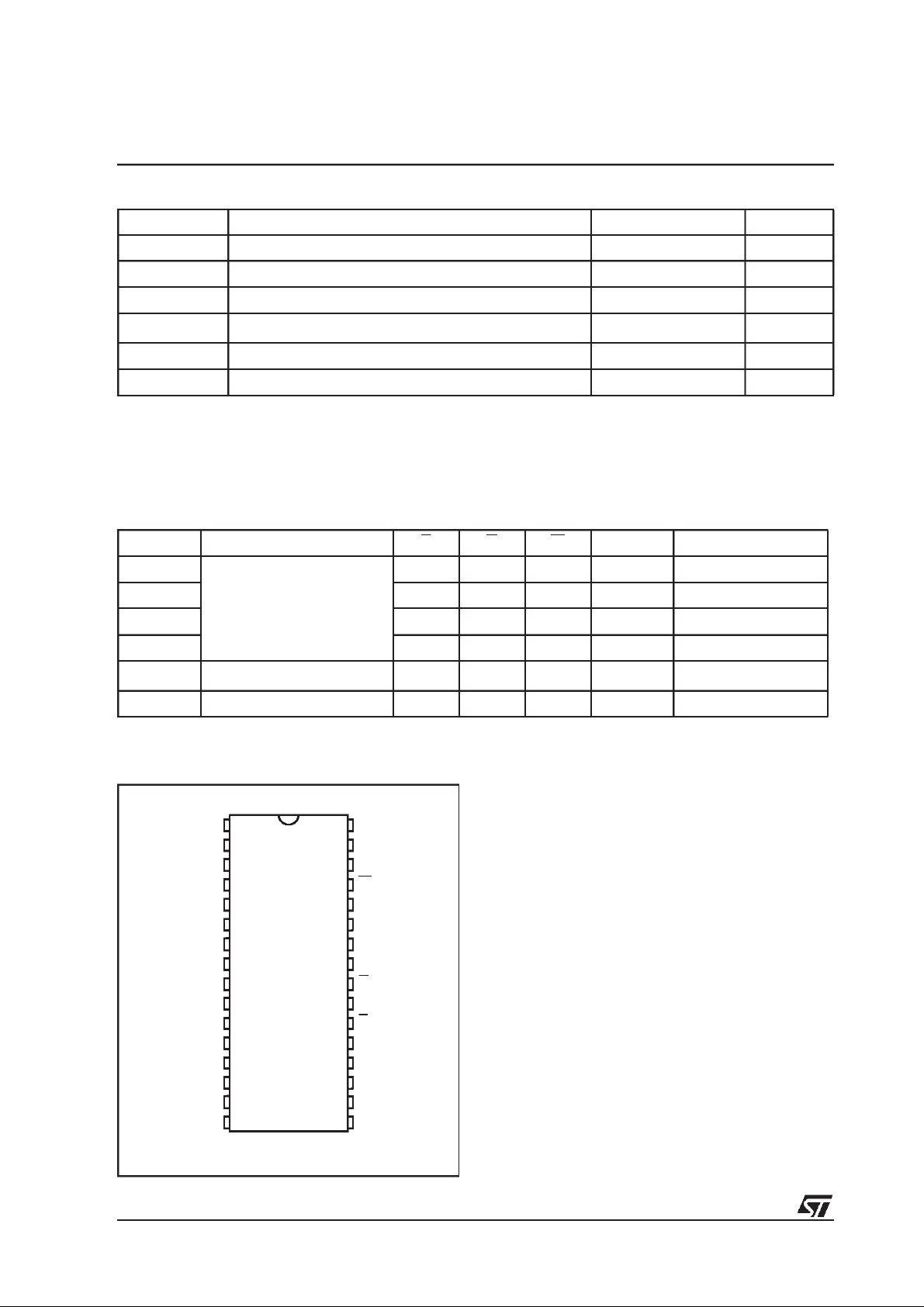
PMDIP32 (PM)
Module
TSOP32
(8 x 20mm)
Surface Mount Chip Set Solution (CS)
Figure 1. Logic Diagram
V
CC
M48Z128
M48Z128Y
SNAPHAT (SH)
Battery
SOH28
Table 1. Signal Names
A0-A16 Address Inputs
DQ0-DQ7 Data Inputs / Outputs
E Chip Enable
G Output Enable
W Write Enable
V
CC
V
SS
NC Not Connected Internally
Supply Voltage
Ground
A0-A16
W
17
M48Z128
M48Z128Y
E
G
V
SS
8
DQ0-DQ7
AI01194
1/17June 2000
M48Z128, M48Z128Y
Table 2. Absolute Maximum Ratings
Symbol Parameter Value Unit
T
A
T
STG
T
BIAS
(2)
T
SLD
V
IO
V
CC
Note: 1. Stresses greater than those listed under ”Absolute Maximum Ratings” may cause permanent damage to thedevice. This is astress
rating only and functional operation of the device at these or any other conditions above those indicated in the operational section
of this specification is not implied. Exposure to the absolute maximum rating conditions for extended periods of time may affect
reliability.
2. Soldering temperature not to exceed 260°C for 10 seconds (total thermal budget not to exceed 150°C for longer than 30 seconds).
CAUTION: Negative undershoots below –0.3V are not allowed on any pin while in the Battery Back-up mode.
Ambient Operating Temperature 0 to 70 °C
Storage Temperature(VCCOff)
Temperature Under Bias –10 to 70 °C
Lead Solder Temperature for 10 seconds 260 °C
Input or Output Voltages –0.3 to 7 V
Supply Voltage –0.3 to 7 V
(1)
–40 to 70 °C
Table 3. Operating Modes
Mode
Deselect
Write
Read
Read V
Deselect
Deselect ≤ V
Note: 1. X = VIHor VIL;VSO= Battery Back-up Switchover Voltage.
V
CC
4.75V to 5.5V
or
4.5V to 5.5V
to V
V
SO
PFD
(min)
SO
E G W DQ0-DQ7 Power
V
IH
V
IL
V
IL
IL
X X X High Z CMOS Standby
X X X High Z Battery Back-up Mode
X X High Z Standby
X
V
IL
V
IH
V
IL
V
IH
V
IH
D
IN
D
OUT
High Z Active
Active
Active
Figure 2. DIP Connections
NC V
1
A16
2
A14
A12
4
A7
5
A6
6
A5
7
A4
A3
A2
A1
A0
DQ0
DQ2
SS
2/17
M48Z128
8
M48Z128Y
9
10
11
12
13
14
15
16
32
31
30
29
28
27
26
25
24
23
22
21
20
19
18
17
AI01195
CC
A15
NC3
W
A13
A8
A9
A11
G
A10
E
DQ7
DQ6
DQ5DQ1
DQ4
DQ3V
DESCRIPTION
The M48Z128/128Y ZEROPOWERRAM is a
128 Kbit x8 non-volatile static RAM thatintegrates
power-fail deselect circuitry and battery control
logic on a single die. The monolithic chip is availablein two special packagesto provide ahighly integrated battery backed-up memory solution.
The M48Z128/128Y is a non-volatile pin andfunction equivalent to any JEDEC standard 128K x8
SRAM. Italso easily fits into many ROM, EPROM,
and EEPROM sockets, providing the non-volatility
of PROMs without any requirement for special
write timing or limitations on the number of writes
that can be performed. The 32 pin 600mil DIP
Module houses the M48Z128/128Y silicon with a
long life lithiumbutton cell in a single package.
Forsurface mountenvironments STprovidesa Chip
Set solution consisting of a 28 pin 330mil SOIC
NVRAMSupervisor (M40Z300) and a 32 pin TSOP
(8x 20mm) LPSRAM (M68Z128) packages.
The 28 pin 330mil SOIC provides sockets with
gold plated contacts at both ends for direct connection to a separate SNAPHAT housing containing the battery.
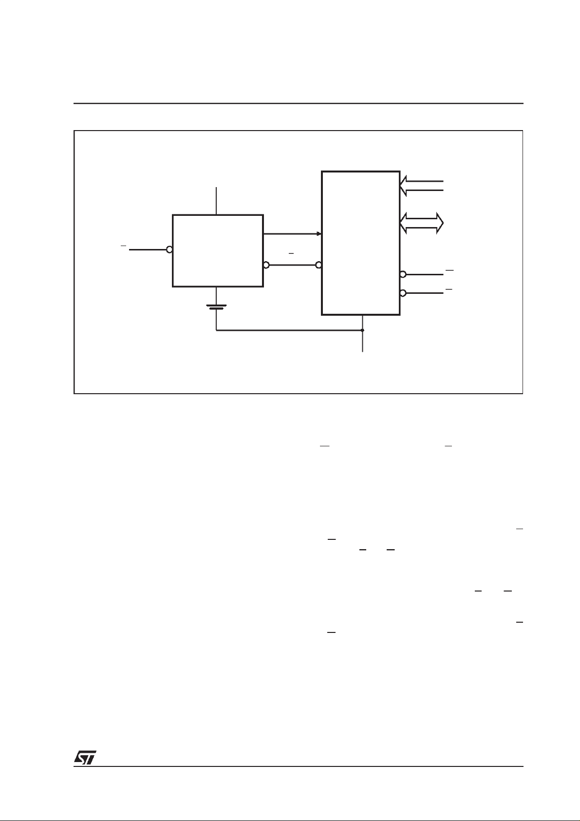
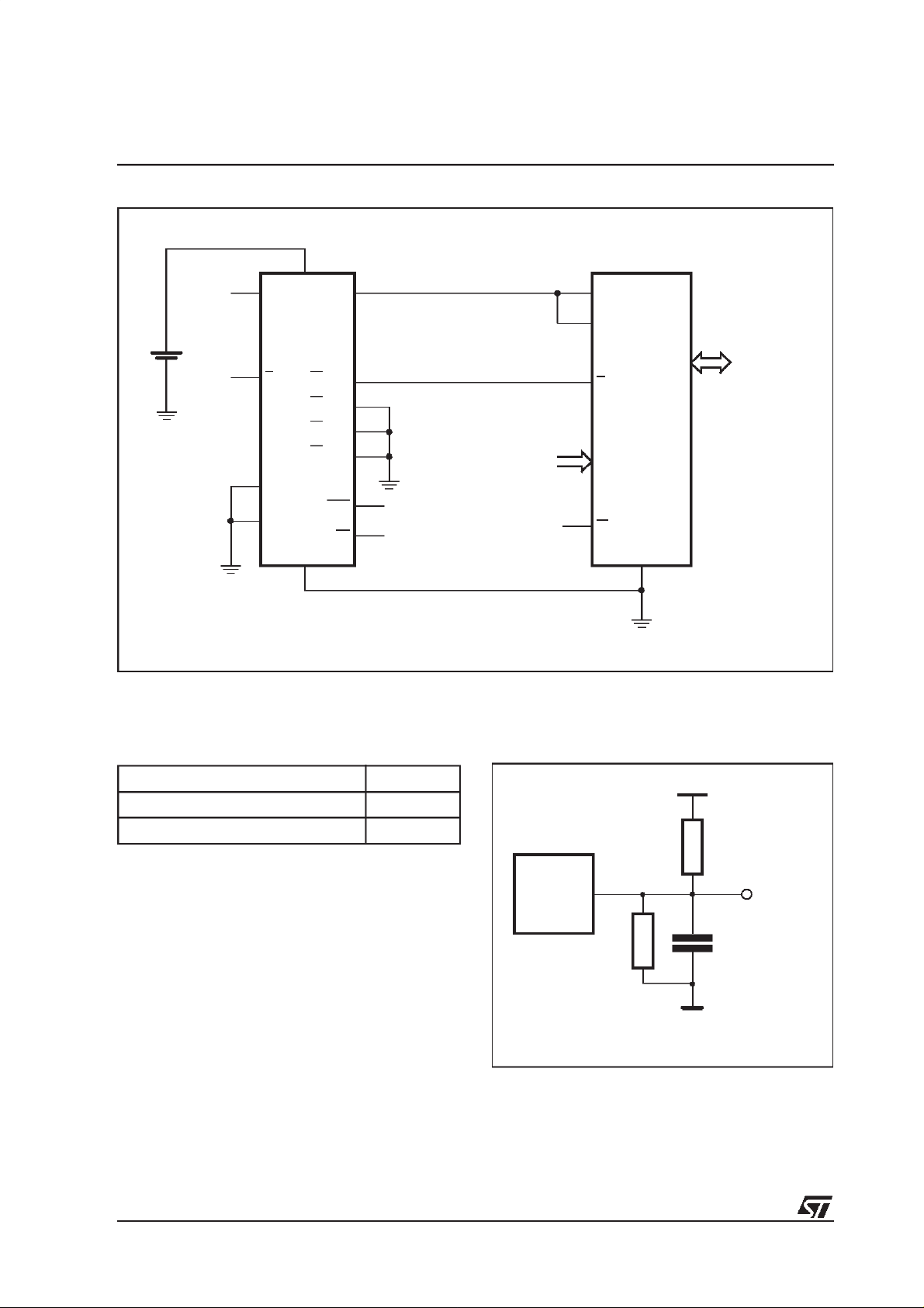
Figure 3. Block Diagram
M48Z128, M48Z128Y
V
CC
A0-A16
POWER
VOLTAGE SENSE
E
AND
SWITCHING
CIRCUITRY
INTERNAL
BATTERY
The unique design allows the SNAPHAT battery
package to be mounted on top of the SOIC package after the completion of the surface mount process. Insertion of the SNAPHAT housing after
reflow prevents potential battery damage due to
the hightemperatures required for device surfacemounting. The SNAPHAT housing is keyed to prevent reverse insertion.
The SNAPHAT battery package is shipped separately in plastic anti-static tubes or in Tape & Reel
form. The part number is ”M4Z28-BRxxSH1”.
The M48Z128/128Y also has its own Power-fail
Detect circuit.The control circuitry constantly monitors the single 5V supply for an out of tolerance
condition. When VCCis out of tolerance, the circuit
write protects the SRAM, providing a high degree
of data security in the midst of unpredictable system operation broughton by low VCC.AsVCCfalls
below approximately 3V, the control circuitry connects the battery which maintains data until valid
power returns.
131,072 x
SRAM ARRAY
E
8
V
SS
DQ0-DQ7
W
G
AI01196
READ MODE
The M48Z128/128Y is in the Read Mode whenever W (Write Enable) is high and E (Chip Enable) is
low. The device architecture allows ripple-through
access of datafrom eight of 1,048,576 locations in
the static storage array. Thus, the unique address
specified by the 17 Address Inputs defines which
oneof the 131,072 bytes of data istobe accessed.
Valid data will be available at the Data I/O pins
within Address Access time (t
) after the last
AVQV
address input signal is stable, providing that the E
and G (Output Enable) access times are also satisfied. If the Eand G access times are notmet, valid data will be available after the later of Chip
Enable Access time (t
cess Time (t
). The state of the eight three-
GLQV
) or Output Enable Ac-
ELQV
state Data I/O signals is controlled by E and G. If
the outputs are activated before t
AVQV
lines will be driven to an indeterminate state until
t
. If the Address Inputs are changed while E
AVQV
and G remain low, output data will remain valid for
Output Data Hold time (t
) but will go indeter-
AXQX
minate until the next Address Access.
, the data
3/17
M48Z128, M48Z128Y
Figure 4. Hardware Hookup for SMT Chip Set
(2)
M40Z300
E1
E2
E3
E4
V
SS
V
CON
CON
CON
CON
OUT
RST
BL
SNAPHAT
BATTERY
THS
(3)
E
A
B
(1)
V
CC
E2
M68Z128
E
A0-A16
W
DQ0-DQ7
V
SS
AI03625
Note: 1. For pin connections, see individual data sheets for M40Z300 and M68Z128 at www.st.com.
2. Connect THS pin toV
3. SNAPHAT ordered separately.
Table 4. AC MeasurementConditions
OUT
if 4.2V ≤ V
≤ 4.5V (M48Z128Y) or connect THS pin to VSSif 4.5V ≤ V
PFD
Figure 5. AC Testing Load Circuit
Input Rise and Fall Times ≤ 5ns
Input Pulse Voltages 0 to 3V
Input and Output Timing Ref. Voltages 1.5V
Note that OutputHi-Z is defined as thepoint where datais no longer
driven.
DEVICE
UNDER
TEST
1kΩ
CLincludes JIG capacitance
≤ 4.75V (M48Z128).
PFD
5V
1.9kΩ
CL= 100pF or
OUT
5pF
AI01030
4/17
M48Z128, M48Z128Y
Table 5. Capacitance
(1, 2)
(TA=25°C, f = 1MHz)
Symbol Parameter Test Condition Min Max Unit
V
V
IN
OUT
=0V
=0V
10 pF
10 pF
C
IN
C
IO
Note: 1. Effective capacitance measured with power supply at 5V.
2. Sampled only, not 100% tested.
3. Outputs deselected.
Input Capacitance
(3)
Input / Output Capacitance
Table 6. DC Characteristics
(TA= 0 to 70 °C; VCC= 4.75V to 5.5V or 4.5V to 5.5V)
Symbol Parameter Test Condition Min Max Unit
(1)
I
LI
I
LO
I
CC
I
CC1
I
CC2
V
IL
V
IH
V
OL
V
OH
Note: 1. Outputs deselected.
Input Leakage Current
(1)
Output Leakage Current
Supply Current
Supply Current (Standby)TTL
Supply Current (Standby)CMOS E ≥ VCC– 0.2V 4 mA
Input Low Voltage –0.3 0.8 V
Input High Voltage 2.2
Output Low Voltage
Output High Voltage
0V ≤ V
0V ≤ V
E=V
I
OL
I
≤ V
IN
CC
≤ V
OUT
, Outputs open
IL
E=V
IH
= 2.1mA
= –1mA
OH
CC
±1 µA
±1 µA
105 mA
7mA
V
+ 0.3
CC
0.4 V
2.4 V
V
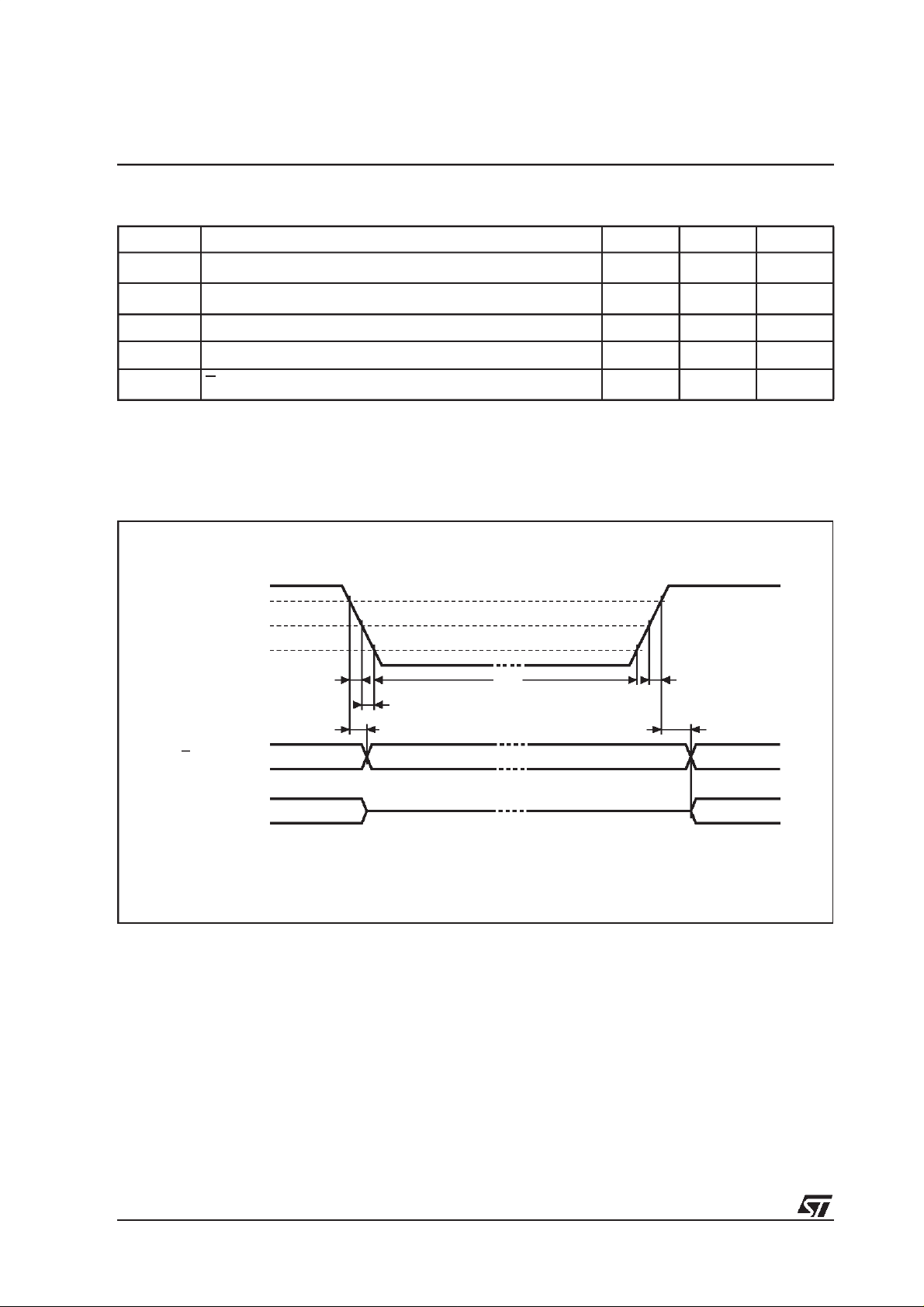
Table 7. Power Down/UpTripPoints DC Characteristics
(1)
(TA= 0 to 70 °C)
Symbol Parameter Min Typ Max Unit
V
PFD
V
SO
t
DR
Note: 1. All voltages referenced to VSS.
2. At 25 °C.
Power-fail Deselect Voltage
Battery Back-up Switchover Voltage 3 V
(2)
Data Retention Time 10 YEARS
M48Z128 4.5 4.6 4.75 V
M48Z128Y 4.2 4.3 4.5 V
5/17
M48Z128, M48Z128Y
Table 8. Power Down/Up AC Characteristics
(TA= 0 to 70 °C)
Symbol Parameter Min Max Unit
(1)
t
F
t
FB
t
WP
t
R
V
(max) to V
(2)
PFD
V
(min) to VSOVCCFallTime
PFD
PFD
Write Protect Time from VCC=V
VSOto V
(max) VCCRise Time
PFD
(min) VCCFall Time 300 µs
10 µs
PFD
40 150 µs
0 µs
t
ER
Note: 1. V
2. V
E Recovery Time 40 120 ms
(max) toV
PFD
(min).
es V
PFD
(min) to VSOfall time of less than tFBmay cause corruption of RAM data.
PFD
(min) falltime of less than tFmay result indeselection/write protection not occurring until 200µs after VCCpass-
PFD
Figure 6. Power Down/Up Mode AC Waveforms
V
CC
V
(max)
PFD
V
(min)
PFD
V
SO
tF
tFB
tWP
E
OUTPUTS
VALID VALID
(PER CONTROLINPUT)
tDR
DON’T CARE
HIGH-Z
tR
tER
RECOGNIZEDRECOGNIZED
(PER CONTROLINPUT)
6/17
AI01031
 Loading...