

SGS Thomson Microelectronics M48Z02, M48Z12-150PC1, M48Z12, M48Z02-70PC1, M48Z02-200PC1 Datasheet
...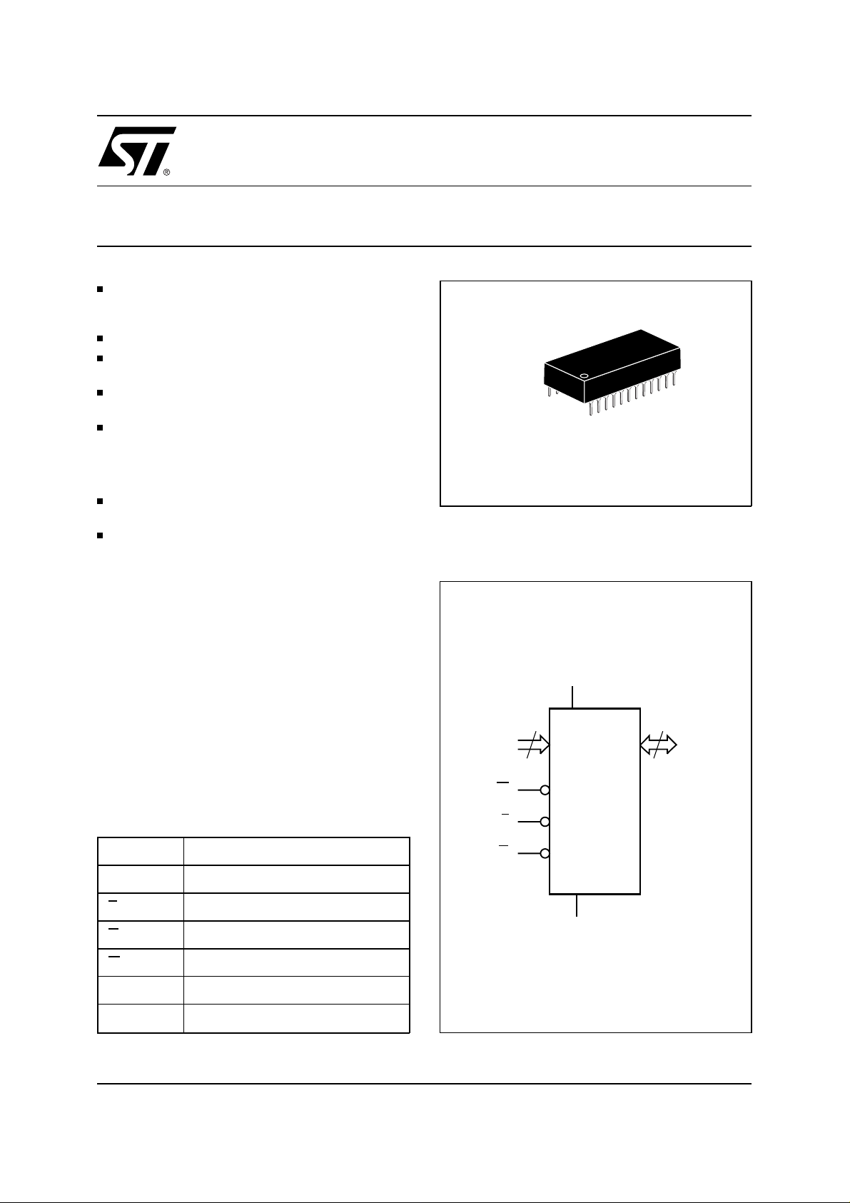
16 Kbit (2Kb x 8) ZEROPOWER® SRAM
INTEGRATED ULTRA LOW POWER SRAM,
POWER-FAIL CONTROL CIRCUIT and
BATTERY
UNLIMITED WRITE CYCLES
READ CYCLE TIME EQUALS WRITE CYCLE
TIME
AUTOMATIC P OWER-F AIL CHIP DES ELECT and
WRITE PROTECTION
WRITE PROTECT VOLT AGES
= Power-fail Deselect Voltage):
(V
PFD
– M48Z02: 4.50V ≤ V
– M48Z12: 4.20V ≤ V
SELF-CONTAINED BATTERY in the CAPHAT
DIP PACKAGE
PIN and FUNCTION COMPATIBLE with
JEDEC STANDARD 2K x 8 SRAMs
DESCRIPTION
The M48Z02/12 ZEROPOWER
non-volatile static RAM which is pin and functional
compatible with the DS1220.
A special 24 pin 600mil DIP CAPHAT package
houses the M48Z02/12 silicon with a long life lithium button cell to form a highly integrated battery
backed-up memory solution.
The M48Z02/12 button cell has sufficient capacity
and storage life to maintain data and clock functionality for an accumulated time period of at least 10
years in the absence of power over the oper ating
temperature range.
T ab le 1. Signal Names
PFD
PFD
4.75V
≤
4.50V
≤
®
RAM is a 2K x 8
24
1
PCDIP24 (PC)
Battery CAPHAT
Figure 1. Logic Diagram
V
CC
11
A0-A10
W
E
M48Z02
M48Z12
M48Z02
M48Z12
8
DQ0-DQ7
A0-A10 Address Inputs
DQ0-DQ7 Data Inputs / Outputs
E Chip Enable
G Output Enable
W Write Enable
V
CC
V
SS
May 1999 1/12
Supply Voltage
Ground
G
V
SS
AI01186
M48Z02, M48Z12
T ab le 2. Absolute Maximum Ratings
(1)
Symbol Parameter Value Unit
T
A
T
STG
(2)
T
SLD
V
IO
V
CC
I
O
P
D
Notes:
1. Stresses greater than those listed under "Absolute Maximum Ratings" may cause permanent damage to the device. This is a
stress rating only and functional operation of the device at these or any other conditions above those indi cat ed in the operati onal
section of this specification is not implied. Exposure to the absolute maximum rating conditions for extended periods of time may
affect reliability.
2. Soldering temperature not to exceed 260°C for 10 seconds (total thermal budget not to exceed 150°C for longer than 30 seconds).
CAUTION: Negat i ve undershoots below –0.3 volts are not allowed on any pin while in the Battery Back-up mode.
Ambient Operating Temperature –40 to 85 °C
Storage T emper ature (VCC Off) –40 to 85 °C
Lead Solder Temperature for 10 seconds 260 °C
Input or Output Voltages –0.3 to 7 V
Supply Voltage –0.3 to 7 V
Output Current 20 mA
Power Dissipation 1 W
T ab le 3. Operating Modes
Mode V
CC
Deselect
Write V
Read V
4.75V to 5.5V
or
4.5V to 5.5V
Read V
Deselect V
Deselect ≤ V
Notes
: X = V
IH
to V
SO
or VIL; VSO = Battery Back-up Switchover Voltage.
(min) X X X High Z CMOS Standby
PFD
SO
E G W DQ0-DQ7 Power
V
IH
IL
IL
IL
X X High Z Standby
XVILD
V
IL
V
IH
V
IH
V
IH
IN
D
OUT
High Z Active
Active
Active
X X X High Z Battery Back-up Mode
Figure 2. DIP Pin Connections
24
23
22
21
20
19
18
17
16
15
14
13
AI01187
2/12
A7
A6
A5
A4
A3
A2
A1
A0
DQ0
DQ2
SS
1
2
3
4
5
6
7
8
9
10
11
12
M48Z02
M48Z12
V
CC
A8
A9
W
G
A10
E
DQ7
DQ6
DQ5DQ1
DQ4
DQ3V
DESCRIPTION
(cont’d)
The M48Z02/12 is a non-volatile pin and function
equivalent to any JEDEC standard 2K x 8 SRAM.
It also easily fits into many ROM, EPROM, and
EEPROM sockets, providing the non-volatility of
PROMs without any requirement for special write
timing or limitations on the number of writes that
can be performed.
The M48Z02/12 also has its own Power-fail Detect
circuit. The control circuitry constantly monitors the
single 5V supply for an out of tolerance condition.
When V
is out of tolerance, the circuit write
CC
protects the SRAM, providing a high degree of data
security in the midst of unpr edictable system operation brought on by low V
. As VCC falls below
CC
approximately 3V , the control circuitry connects the
battery which maintains data and clock operation
until valid power returns.
Figure 3. Block Diagram
M48Z02, M48Z12
A0-A10
LITHIUM
CELL
VOLTAGE SENSE
AND
SWITCHING
CIRCUITRY
V
CC
READ MODE
The M48Z02/12 is in the Read Mode whenever
(Write Enable) is high and
E (Chip Enable) is low.
W
The device architecture allows ripple-through access of data from eight of 16,384 locations in the
static storage array. Thus, the unique address
specified by the 11 Address Inputs defines which
one of the 2,048 bytes of data is to be accessed.
Valid data will be available at the Data I/O pins
within Address Access time (t
) after the last
AVQV
address input signal is stable, providing that the
G access times are also satisfied. If the E and
and
G access times are not met, valid data will be
available after the latter of the Chip Enable Access
time (t
) or Output Enable Access time (t
ELQV
GLQV
The state of the eight three-state Data I/O signals
is controlled by
before t
AVQ V
indeterminate state until t
puts are changed while
E and G. If the outputs are activated
, the data lines will be driven to an
. If the Address In-
AVQV
E and G remain active,
output data will remain valid for Output Data Hold
time (t
) but will go indeterminate until the next
AXQX
Addres s Access.
POWER
V
PFD
2K x 8
SRAM ARRAY
V
SS
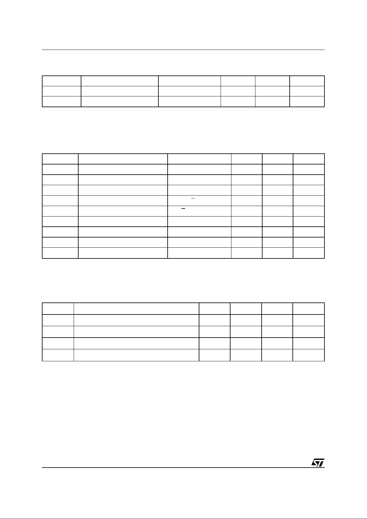
Table 4. AC Measurement Conditions
Input Rise and Fall Times ≤ 5ns
Input Pulse Voltages 0V to 3V
Input and Output Timing Ref. Voltages 1.5V
Note that Output Hi-Z is defined as the point where data is no
longer driven.
Figure 4. AC Testing Load Circuit
E
).
DEVICE
UNDER
TEST
1kΩ
DQ0-DQ7
E
W
G
AI01255
5V
1.8kΩ
OUT
CL = 100pF
CL includes JIG capacitance
AI01019
3/12
M48Z02, M48Z12
(1)
T ab le 5. Capacitance
= 25 °C)
(T
A
Symbol Parameter T est Condition Min Max Unit
C
IN
(2)
C
IO
Notes:
1. Effective capacitance measured with power supply at 5V .
2. Outputs deselected
Input Capacitance VIN = 0V 10 pF
Input / Output Capacitance V
= 0V 10 pF
OUT
T ab le 6. DC Characteristics
= 0 to 70°C or –40 to 85°C; VCC = 4.75V to 5.5V or 4.5V to 5.5V)
(T
A
Symbol Parameter Test Condition Min Max Unit
(1)
I
LI
(1)
I
LO
Supply Current Outputs open 80 mA
I
CC
I
CC1
I
CC2
(2)
V
IL
V
IH
V
OL
V
OH
Notes:
1. Outputs Deselected.
2. Negative spikes of –1V allowed for up to 10ns once per cycle.
T able 7. Power Down/Up Trip Points DC Characteristics
= 0 to 70°C or –40 to 85°C)
(T
A
Input Leakage Current 0V ≤ VIN ≤ V
Output Leakage Current 0V ≤ V
Supply Current (Standby) TTL E = V
Supply Current (Standby) CMOS E = VCC – 0.2V 3 mA
OUT
≤ V
IH
CC
CC
Input Low Voltage –0.3 0.8 V
Input High Voltage 2.2 VCC + 0.3 V
Output Low Voltage IOL = 2.1mA 0.4 V
Output High Voltage IOH = –1mA 2.4 V
(1)
±1 µA
±5 µA
3mA
Symbol Parameter Min Typ Max Unit
V
PFD
V
PFD
V
SO
t
DR
Note:
1. All voltages referenced to V
Power-fail Deselect Voltage (M48Z02) 4.5 4.6 4.75 V
Power-fail Deselect Voltage (M48Z12) 4.2 4.3 4.5 V
Battery Back-up Switchover Voltage 3.0 V
Expected Data Retention Time 10 YEARS
4/12
.
SS
 Loading...