

5.0 or 3.3V, 4096K TIMEKEEPER® SRAM with PHANTOM
FEATURES SUMMARY
■ 5.0V OR 3.3V OPERATING VOLTAGE
■ REAL TIME CLOCK KEEPS TRACK OF
TENTHS/HUNDREDTHS OF SECONDS,
SECONDS, MINUTES, HOURS, DAYS, DATE
OF THE MONTH, MONTHS, and YEARS
■ AUTOMATIC LEAP YEAR CORRECTION
VALID UP TO THE YEAR 2100
■ AUTOMATIC SWITCH-OVER and DESELECT
CIRCUITRY
■ CHOICE OF POWER-FAIL DESELECT
VOLTAGES:
= Power-fail Deselect Voltage):
(V
PFD
– M48T251Y: 4.25V
– M48T251V: 2.80V
■ FULL 10% V
■ OVER 10 YEARS’ DATA RETENTION IN THE
CC
≤ V
≤ V
OPERATING RANGE
ABSENCE OF POWER
■ WATCH FUNCTION IS TRANSPARENT TO
RAM OPERATION
■ 512K x 8 NV SRAM DIRECTLY REPLACES
VOLATILE STAT IC RA M OR EEPRO M
PFD
PFD
≤ 4.50V
≤ 2.97V
M48T251Y
M48T251V
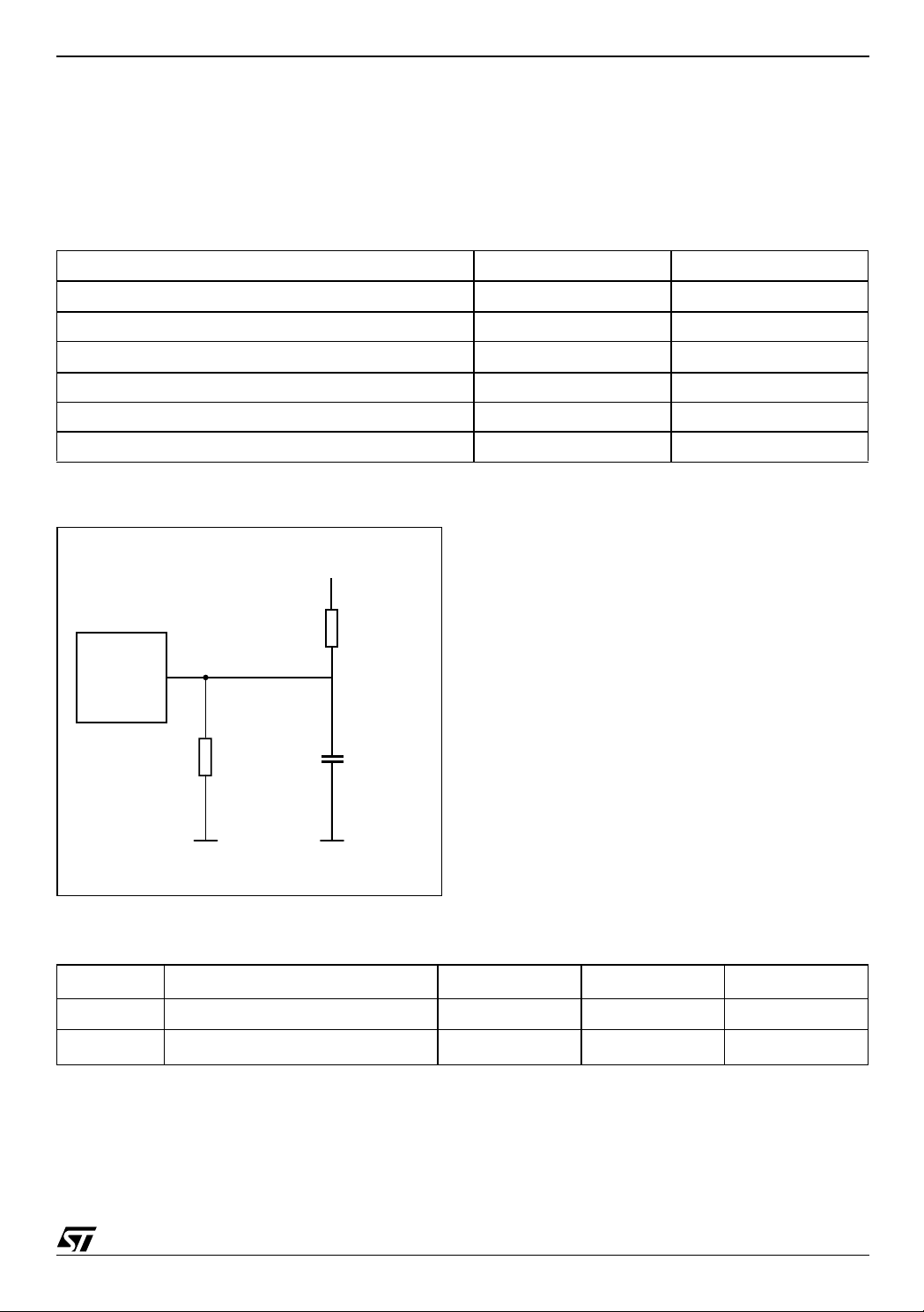
Figure 1. 32-pin, DIP Package
32
1
PMDIP32 (PM)
Rev. 2.0
1/24March 2003

M48T251Y, M48T251V
TABLE OF CONTENTS
SUMMARY DESCRIPTION. . . . . . . . . . . . . . . . . . . . . . . . . . . . . . . . . . . . . . . . . . . . . . . . . . . . . . . . . . . 4
Figure 2. Logic Diagram . . . . . . . . . . . . . . . . . . . . . . . . . . . . . . . . . . . . . . . . . . . . . . . . . . . . . . . . . . 4
Table 1. Signal Names . . . . . . . . . . . . . . . . . . . . . . . . . . . . . . . . . . . . . . . . . . . . . . . . . . . . . . . . . . . 4
Figure 3. DIP Connections . . . . . . . . . . . . . . . . . . . . . . . . . . . . . . . . . . . . . . . . . . . . . . . . . . . . . . . . 4
Figure 4. Block Diagram . . . . . . . . . . . . . . . . . . . . . . . . . . . . . . . . . . . . . . . . . . . . . . . . . . . . . . . . . . 5
MAXIMUM RATING. . . . . . . . . . . . . . . . . . . . . . . . . . . . . . . . . . . . . . . . . . . . . . . . . . . . . . . . . . . . . . . . . 6
Table 2. Absolute Maximum Ratings. . . . . . . . . . . . . . . . . . . . . . . . . . . . . . . . . . . . . . . . . . . . . . . . . 6
DC AND AC PARAMETERS. . . . . . . . . . . . . . . . . . . . . . . . . . . . . . . . . . . . . . . . . . . . . . . . . . . . . . . . . . 7
Table 3. DC and AC Measurement Conditions . . . . . . . . . . . . . . . . . . . . . . . . . . . . . . . . . . . . . . . . . 7
Figure 5. AC Testing Load Circuit . . . . . . . . . . . . . . . . . . . . . . . . . . . . . . . . . . . . . . . . . . . . . . . . . . . 7
Table 4. Capacitance. . . . . . . . . . . . . . . . . . . . . . . . . . . . . . . . . . . . . . . . . . . . . . . . . . . . . . . . . . . . . 7
Table 5. DC Characteristics. . . . . . . . . . . . . . . . . . . . . . . . . . . . . . . . . . . . . . . . . . . . . . . . . . . . . . . . 8
OPERATION MODES . . . . . . . . . . . . . . . . . . . . . . . . . . . . . . . . . . . . . . . . . . . . . . . . . . . . . . . . . . . . . . . 9
Table 6. Operating Modes. . . . . . . . . . . . . . . . . . . . . . . . . . . . . . . . . . . . . . . . . . . . . . . . . . . . . . . . . 9
READ . . . . . . . . . . . . . . . . . . . . . . . . . . . . . . . . . . . . . . . . . . . . . . . . . . . . . . . . . . . . . . . . . . . . . . . . 9
WRITE. . . . . . . . . . . . . . . . . . . . . . . . . . . . . . . . . . . . . . . . . . . . . . . . . . . . . . . . . . . . . . . . . . . . . . . . 9
Figure 6. Memory READ Cycle . . . . . . . . . . . . . . . . . . . . . . . . . . . . . . . . . . . . . . . . . . . . . . . . . . . . . 9
Figure 7. Memory WRITE Cycle 1 . . . . . . . . . . . . . . . . . . . . . . . . . . . . . . . . . . . . . . . . . . . . . . . . . .10
Figure 8. Memory WRITE Cycle 2 . . . . . . . . . . . . . . . . . . . . . . . . . . . . . . . . . . . . . . . . . . . . . . . . . .11
Table 7. Memory AC Characteristics, M48T251Y . . . . . . . . . . . . . . . . . . . . . . . . . . . . . . . . . . . . . . 12
Table 8. Memory AC Characteristics, M48T251V . . . . . . . . . . . . . . . . . . . . . . . . . . . . . . . . . . . . . . 13
Data Retention Mode. . . . . . . . . . . . . . . . . . . . . . . . . . . . . . . . . . . . . . . . . . . . . . . . . . . . . . . . . . . 14
Figure 9. Power Down/Up Mode AC Waveforms . . . . . . . . . . . . . . . . . . . . . . . . . . . . . . . . . . . . . . 14
Table 9. Power Down/Up Trip Points DC Characteristics . . . . . . . . . . . . . . . . . . . . . . . . . . . . . . . . 14
PHANTOM CLOCK OPERATION. . . . . . . . . . . . . . . . . . . . . . . . . . . . . . . . . . . . . . . . . . . . . . . . . . . . .15
Figure 10. Comparison Register Definition . . . . . . . . . . . . . . . . . . . . . . . . . . . . . . . . . . . . . . . . . . . 16
Clock Register Information. . . . . . . . . . . . . . . . . . . . . . . . . . . . . . . . . . . . . . . . . . . . . . . . . . . . . . 17
Clock Accuracy . . . . . . . . . . . . . . . . . . . . . . . . . . . . . . . . . . . . . . . . . . . . . . . . . . . . . . . . . . . . . . . 17
AM-PM/12/24 Mode . . . . . . . . . . . . . . . . . . . . . . . . . . . . . . . . . . . . . . . . . . . . . . . . . . . . . . . . . . . . 17
Oscillator and Reset Bits . . . . . . . . . . . . . . . . . . . . . . . . . . . . . . . . . . . . . . . . . . . . . . . . . . . . . . . 17
2/24

M48T251Y, M48T251V
Zero Bits. . . . . . . . . . . . . . . . . . . . . . . . . . . . . . . . . . . . . . . . . . . . . . . . . . . . . . . . . . . . . . . . . . . . . 17
Table 10. Phantom Clock Register Map . . . . . . . . . . . . . . . . . . . . . . . . . . . . . . . . . . . . . . . . . . . . . 17
Figure 11. Phantom Clock READ Cycle . . . . . . . . . . . . . . . . . . . . . . . . . . . . . . . . . . . . . . . . . . . . . 18
Figure 12. Phantom Clock WRITE Cycle . . . . . . . . . . . . . . . . . . . . . . . . . . . . . . . . . . . . . . . . . . . . 18
Figure 13. Phantom Clock Reset. . . . . . . . . . . . . . . . . . . . . . . . . . . . . . . . . . . . . . . . . . . . . . . . . . . 18
Table 11. Phantom Clock AC Characteristics (M48T251Y) . . . . . . . . . . . . . . . . . . . . . . . . . . . . . . 19
Table 12. Phantom Clock AC Characteristics (M48T251V) . . . . . . . . . . . . . . . . . . . . . . . . . . . . . . 20
PACKAGE MECHANICAL INFORMATION . . . . . . . . . . . . . . . . . . . . . . . . . . . . . . . . . . . . . . . . . . . . . 21
PART NUMBERING . . . . . . . . . . . . . . . . . . . . . . . . . . . . . . . . . . . . . . . . . . . . . . . . . . . . . . . . . . . . . . . 22
REVISION HISTORY. . . . . . . . . . . . . . . . . . . . . . . . . . . . . . . . . . . . . . . . . . . . . . . . . . . . . . . . . . . . . . . 23
3/24
M48T251Y, M48T251V
SUMMARY DESCRIPTION
®
The M48T251Y/V TIMEKEEPER
512Kbit x 8 non-volatile static RAM and real time
clock organized as 524 ,288 words by 8 bits. The
special DIP package provides a fully integrated
battery back-up memory and real time clock solution. In the event of power instability or absence, a
self-contained battery maintains the timekeeping
operation and provides po wer for a CMOS static
RAM. Control circuitry monitors V
write protection to prevent data c orruption in the
memory and RTC.
The clock keeps track of tenths/hundredths of seconds, seconds, minutes , hou rs, day, date, month,
RAM is a
and invokes
CC
and year information. The last day of the month is
automatically adjusted for months with less than
31 days, including leap year correction.
The clock operates in one of two formats:
– a 12-hour mode with an AM/PM indicator; or
– a 24-hour mode
The M48T251Y/V is a 32-pin (PM) DIP module
that integrates the RTC, the battery, and SRAM in
one package.
The modules are shipped in plastic, anti-static
tubes (see Table 14, page 22).
Figure 2. Logic Diagram Table 1. Signal Names
A0–A18 Address Input
RST
CE
OE
WE
Reset Input
Chip Enable
Output Enable Input
WRITE Enable Input
DQ0–DQ7 Data Inputs/Outputs
V
CC
V
SS
Supply Voltage Input
Ground
A0-A18
WE
CE
OE
V
CC
M48T251Y
M48T251V
DQ0-D7
RST
Figure 3. DIP C on ne ctions
V
30
29
28
27
26
25
24
23
22
20
19
18
17
32
31
21
CC
A15
A17
WE
A13
A8
A9
A11
OE
A10
CE
DQ7
DQ6
DQ5
DQ4
DQ3
AI04239
V
SS
AI04237
A18/RST
A16
A14
A12
DQ0
DQ1
DQ2
V
SS
A6
A5
A4
A3
A2
A0
A7
A1
1
2
3
4
5
6
7
8
9
10
11
12
13
14
15
16
M48T251Y
M48T251V
4/24
Figure 4. Block Diagram
M48T251Y, M48T251V
CE
OE
WE
RST
DQ0
CONTROL
LOGIC
ACCESS
ENABLE
SEQUENCE
DETECTOR
I/O
BUFFERS
32.768 Hz
CRYSTAL
READ
WRITE
POWER
FAIL
DATA
XO
XI
CLOCK/CALENDAR
LOGIC
UPDATE
TIMEKEEPER
REGISTER
SRAM
COMPARISON
REGISTER
INTERNAL V
CC
A0–A16
DQ0–DQ7
V
CC
POWER-FAIL
DETECT
LOGIC
V
BAT
AI04238
5/24
M48T251Y, M48T251V
MAXIMUM RATI N G
Stressing the device ab ove the rating listed in t he
“Absolute Maximum Ratings” table may cause
permanent damage to the device. These are
stress ratings only and operation of the dev ice at
these or any other conditions above those indicated in the Operating sections of this specification is
Table 2. Absolute Maximum Ratings
Symbol Parameter Value Unit
T
A
T
STG
(1)
T
SLD
V
CC
V
IO
I
O
P
D
Note: 1. Soldering temperature not to exceed 260°C for 10 seconds (total thermal budget not to exceed 150°C for longer than 30 seconds).
CAUTION! Negative undershoots below -0.3V are not al l owed on any pi n while in th e B attery Back-up Mod e .
Operating Temperature 0 to 70 °C
Storage Temperature (VCC, Oscillator Off)
Lead Solder Temperature for 10 seconds 260 °C
Supply Voltage (on any
pin relative to Ground)
Input or Output Voltages
Output Current 20 mA
Power Dissipation 1 W
not implied. Exposure to Absol ute Maxim um Ra ting conditions for extended periods may affect device reliability. Refer also to the
STMicroelectronics SURE Program and other relevant quality documents.
–40 to 85 °C
M48T251Y –0.3 to +7.0 V
M48T251V –0.3 to +4.6 V
–0.3 to V
CC
+ 0.3
V
6/24
M48T251Y, M48T251V
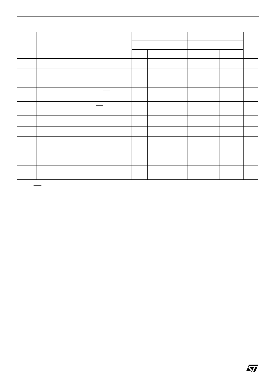
DC AND AC PARAMETERS
This section summarizes the operat ing and measurement conditions, as well as the DC and AC
characteristics of the device. The parameters in
the following DC and AC Characteristic tables are
derived from tests performed under the M easure-
Table 3. DC and AC Measurement Conditions
Parameter M48T251Y M48T251V
V
Supply Voltage
CC
Ambient Operating Temperature 0 to 70°C 0 to 70°C
Load Capacitance (C
Input Rise and Fall Times ≤ 5ns ≤ 5ns
Input Pulse Voltages 0 to 3V 0 to 3V
Input and Output Timing Ref. Voltages 1.5V 1.5V
Note: Out put Hi gh Z is defined as the poi nt where dat a i s no longer driven (see Table 3, page 7).
)
L
Figure 5. AC Testing Load Circuit
ment Conditions listed in the rel evant tables. Designers should check that the operating conditions
in their projects match the measurement conditions when using the quoted parameters.
4.5 to 5.5V 3.0 to 3.6V
100pF 50pF
V
CCI
1.1 KΩ
DEVICE
UNDER
TEST
680 Ω
Note: 50pF f or M48T251V.
CL = 50 pF
AI04240
Table 4. Capacitance
Symbol
C
IN
(3)
C
IO
Note: 1. Effective capacit ance meas ured with po wer supp l y at 5V . S am pled onl y; not 100% tested.
2. At 25°C, f = 1MHz.
3. Outpu ts were deselected.
Input Capacitance 10 pF
Input / Output Capacitance 10 pF
Parameter
(1,2)
Min Max Unit
7/24
M48T251Y, M48T251V
Table 5. DC Characteristics
M48T251Y M48T251V
Sym
(2)
I
LI
I
LO
I
CC1
I
CC2
I
CC3
(3)
V
IL
(3)
V
IH
V
OL
V
OH
(3)
V
PFD
(3)
V
SO
Note: 1. Valid fo r A m bi ent Operating Temperature: TA = 0 to 70°C; VCC = 4.5 to 5.5V or 3. 0 to 3.6V (except wher e not ed).
2. RST
3. All voltages are referenced to Ground.
Parameter
Input Leakage Current
Output Leakage Current
Supply Current 85 50 mA
Supply Current (TTL
Standby)
VCC Power Supply
Current
Input Low Voltage –0.3 0.8 –0.3 0.6 V
Input High Voltage 2.2
Output Low Voltage
Output High Voltage
Power Fail Deselect 4.25 4.37 4.50 2.80 2.97 V
Battery Back-up
Switchover
(Pin 1) has an i nternal pu l l-up resistor.
(1)
Test Condition
0V ≤ V
0V ≤ V
CE
I
IN
OUT
= V
CE
= V
CCI
I
= 2.0 mA
OL
= –1.0 mA
OH
≤ V
≤ V
IH
– 0.2
Min Typ Max Min Typ Max
CC
CC
±1 ±1 µA
±1 ±1 µA
510 5 7mA
35 23mA
V
CC
+ 0.3
2.2
0.4 0.4 V
2.4 2.4 V
V
BAT
2.5 V
VCC + 0.3
Unit–70 –85
V
8/24
 Loading...