

SGS Thomson Microelectronics M48T212Y, M48T212V Datasheet
5V/3.3V TIMEKEEPERCONTROLLER
■ CONVERTS LOW POWER SRAM into
NVRAMs
■ YEAR 2000 COMPLIANT (4-Digit Year)
■ BATTERY LOW FLAG
■ INTEGRATED REAL TIME CLOCK,
POWER-FAIL CONTROLCIRCUIT,BATTERY
and CRYSTAL
■ AUTOMATIC POWER-FAIL CHIP DESELECT
and WRITE PROTECTION
■ WATCHDOG TIMER
■ CHOICE of WRITE PROTECT VOLTAGES
(V
= Power-fail Deselect Voltage):
PFD
– M48T212Y: 4.2V ≤ V
– M48T212V: 2.7V ≤ V
■ MICROPROCESSOR POWER-ON RESET
■ PROGRAMMABLE ALARM OUTPUT ACTIVE
in the BATTERY BACKED-UP MODE
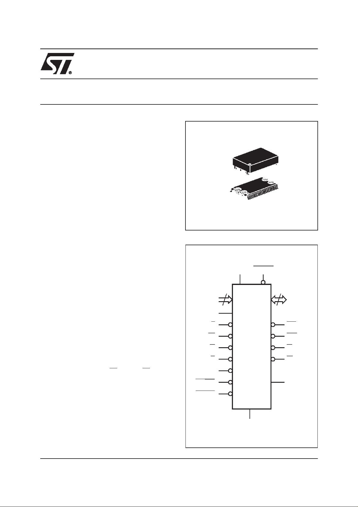
■ PACKAGING INCLUDESa44-LEADSOICand
SNAPHATTOP (to be Ordered Separately)
PFD
PFD
≤ 4.5V
≤ 3.0V
SNAPHAT (SH)
Battery
44
1
SOH44 (MH)
Figure 1. Logic Diagram
V
CC
M48T212Y
M48T212V
V
CCSW
DESCRIPTION
The M48T212Y/V are self-contained devices that
include a real time clock (RTC), programmable
alarms, a watchdog timer, and two external chip
enable outputs which provide control of up to four
(two in parallel) external low-power static RAMs.
Access to all TIMEKEEPERfunctions and the
external RAM is the same as conventional bytewide SRAM. The16TIMEKEEPER Registers offer
Century, Year, Month, Date, Day, Hour, Minute,
Second, Calibration,Alarm, Watchdog,and Flags.
Externally attached static RAMs are controlled by
the M48T212Y/V via the E1
CON
and E2
CON
sig-
nals (see Table 4).
The 44 pin 330mil SOIC provides sockets with
gold plated contacts at both ends for direct connection to a separate SNAPHAT housing containing the battery and crystal. The unique design
allows the SNAPHAT battery package to be
mounted on top of the SOIC package after the
completion of the surface mount process.
A0-A3
EX
W
WDI
RSTIN1
RSTIN2
4
A
E
M48T212Y
M48T212V
G
V
SS
8
DQ0-DQ7
IRQ/FT
RST
E1
CON
E2
CON
V
OUT
AI03019
1/23April 2000
M48T212Y, M48T212V
Figure 2. SOIC Connections
RSTIN1
RSTIN2
RST
NC
NC EX
NC
NC
NC
NC
NC
NC
A3
A2
A1
A0
WDI
E2
CON
DQ1
DQ2
V
SS
1
2
3
4
5
6
7
8
A
9
10
M48T212Y
11
M48T212V
12
13
14
15
16
17
18
19
20
21
22
44
43
42
41
40
39
38
37
36
35
34
33
32
31
30
29
28
27
26
25
24
23
AI03020
V
CC
V
OUT
V
CCSW
IRQ/FT
NC
NC
NC
NC
NC
G
W
NC
NC
E
E1
CON
DQ7
DQ6
DQ5DQ0
DQ4
DQ3
NC
Table 1. Signal Names
A0-A3 Address Inputs
DQ0-DQ7 Data Inputs/Outputs
RSTIN1 Reset 1 Input
RSTIN2 Reset 2 Input
RST Reset Output (Open Drain)
WDI Watchdog Input
A Bank Select Input
E Chip Enable Input
EX External Chip Enable Input
G Output Enable Input
W Write Enable Input
E1
CON
E2
CON
IRQ/FT Int/Freq Test Output (Open Drain)
Vccsw
V
OUT
V
CC
V
SS
NC Not Connected internally
RAM Chip Enable 1 Output
RAM Chip Enable 2 Output
V
Switch Output
CC
Supply Voltage Output
Supply Voltage
Ground
Insertion of the SNAPHAT housing after reflow
prevents potential battery andcrystal damagedue
to the high temperatures required for device surface-mounting. The SNAPHAT housing is keyed
to prevent reverse insertion.
The SOIC and battery/crystal packages are
shipped separately inplastic anti-static tubesor in
Tape & Reel form. For the 44 lead SOIC, the battery/crystal package (i.e. SNAPHAT) part number
is ”M4TXX-BR12SH” (see Table 15).
Caution: Do not placetheSNAPHAT battery/crystal topin conductive foam,as this will drain thelithium button-cell battery.
Automatic backup and write protection for an external SRAM is provided through V
and E2
pins. (Users are urged to insure that
CON
OUT
,E1
CON
voltage specifications, for both the controller chip
and external SRAM chosen, are similar). The
SNAPHAT containing the lithium energy source
used to permanently power the real time clock is
also used to retain RAM data in the absence of
VCCpower through the V
The chip enable outputs to RAM (E1
E2
) are controlled during power transients to
CON
OUT
pin.
CON
and
prevent data corruption. The date is automatically
adjusted for months with less than 31 days and
corrects forleap years. The internalwatchdog timer provides programmable alarm windows.
The nine clock bytes (Fh - 9h and 1h) are not the
actual clock counters, they are memory locations
consisting of BiPORTTMread/write memory cells
within the static RAM array. Clock circuitry updates the clock byteswith current information once
per second. The information can be accessed by
the userin thesame manner asany otherlocation
in the staticmemory array.
Byte 8h isthe clock control register.This byte controls user access to the clock information and also
stores the clock calibration setting. Byte 7h contains the watchdog timer setting. The watchdog
timer can generate either a reset or an interrupt,
depending on the state of the Watchdog Steering
bit (WDS). Bytes 6h-2hinclude bits that,when programmed, provide for clock alarm functionality.
Alarms are activated when the register content
matches the month, date, hours, minutes, and
seconds of the clock registers. Byte 1h contains
century information. Byte 0h contains additional
flag information pertaining to the watchdog timer,
alarm and battery status.
2/23
M48T212Y, M48T212V
Table 2. Absolute Maximum Ratings
(1)
Symbol Parameter Value Unit
T
A
T
STG
T
SLD
V
IO
V
CC
I
O
P
D
Note: 1. Stresses greaterthan those listed under ”Absolute Maximum Ratings” may cause permanent damage to thedevice. This is a stress
rating only and functional operation of the device at these or any other conditions above those indicated in the operational section
of this specification is not implied. Exposure to the absolute maximum rating conditions for extended periods of time may affect
reliability.
2. Soldering temperature not to exceed 260°C for 10 seconds (totalthermal budget not to exceed 150°C for longer than 30 seconds).
CAUTION: Negative undershoots below –0.3V are not allowed on any pin while in the Battery Back-up mode.
CAUTION: Do NOTwave solder SOIC to avoid damaging SNAPHATsockets.
Table 3. Operating Modes
Mode
Deselect
Write
Read
Read
Deselect
Deselect
Note: 1. X = VIHor VIL.
2. V
SO
Ambient Operating Temperature 0 to 70 °C
Storage Temperature (VCCOff, Oscillator Off) SNAPHAT
SOIC
(2)
Lead Solder Temperature for 10 sec 260 °C
–40 to 85
–55 to 125
Input or Output Voltages –0.3 to VCC+0.3 V
Supply Voltage M48T212Y
M48T212V
–0.3 to 7
–0.3 to 4.6
Output Current 20 mA
Power Dissipation 1 W
(1)
V
CC
4.5V to 5.5V
or
3.0V to 3.6V
to V
V
SO
PFD
≤ V
SO
= Battery Back-up Switchover Voltage. (See Tables 7A and 7B fordetails).
(min)
(2)
(2)
E G W DQ7-DQ0 Power
V
IH
V
IL
V
IL
V
IL
X X High-Z Standby
X
V
IL
V
IH
V
IL
V
IH
V
IH
D
IN
D
OUT
High-Z Active
X X X High-Z CMOS Standby
X X X High-Z Battery Back-Up
°C
V
Active
Active
Table 4. Truth Table for SRAM Bank Select
Mode V
Select
Deselect High X High High Standby
Deselect
V
SO
Deselect
Note: 1. X = VIHor VIL.
= Battery Back-up Switchover Voltage. (See Tables 7A and 7B fordetails).
2. V
SO
CC
4.5V to 5.5V
or
3.0V to 3.6V
to V
≤ V
PFD
SO
(min)
(2)
(2)
(1)
EX A E1
CON
E2
CON
Low Low Low High Active
Low High High Low Active
X X High High CMOS Standby
X X High High Battery Back-Up
Power
3/23
M48T212Y, M48T212V
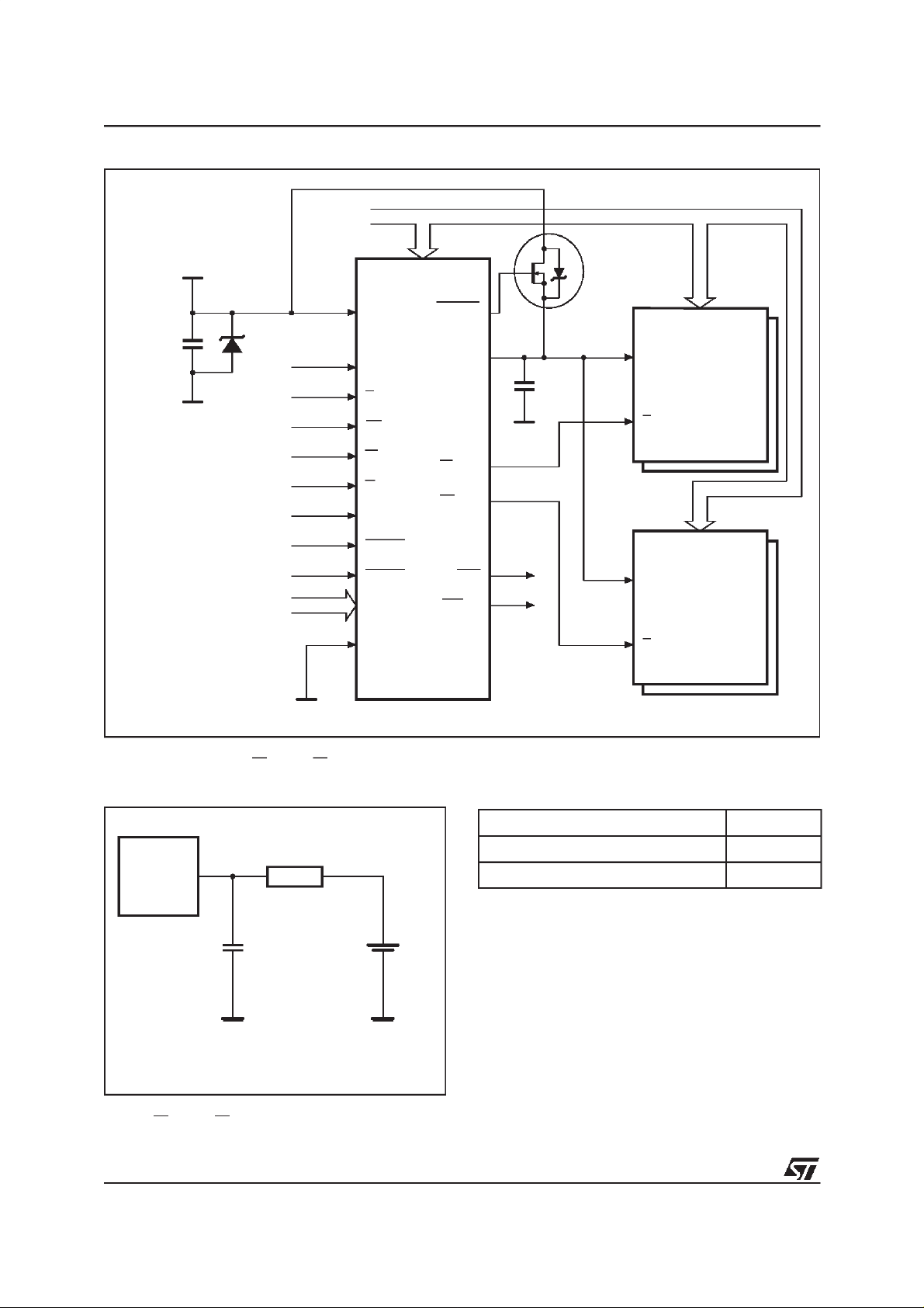
Figure 3. Hardware Hookup
A0-A18
0.1µF
5V/3.3V
1N5817
0.1µF
MOTOROLA
MTD20P06HDL
V
CC
E
V
CC
E
A0-Axx
CMOS
SRAM
A0-Axx
CMOS
SRAM
A0-A3
V
V
CC
(1)
A
E
EX
W
G
WDI
RSTIN1
RSTIN2
DQ0-DQ7
V
SS
M48T212Y/V
CCSW
V
OUT
E1
CON
E2
CON
RST
IRQ/FT
Note 2
Note: 1. See description in Power Supply Decoupling and Undershoot Protection.
2. Traces connecting E1
Figure 4. AC Testing Load Circuit
CON
and E2
to external SRAM should be as short as possible.
CON
Table 5. AC Measurement Conditions
Input Rise and Fall Times ≤ 5ns
DEVICE
UNDER
TEST
645Ω
Input Pulse Voltages 0 to 3V
Input and Output Timing Ref.Voltages 1.5V
Note that Output Hi-Z is defined as the point where data
is no longer driven.
(1)
(2)
1.75V
AI03239
CLincludes JIG capacitance
Note: 1. DQ0-DQ7
2. E1
CON
and E2
CL= 100pF or 5pF
CL=30pF
CON
4/23
AI03046
M48T212Y, M48T212V
Table 6. Capacitance
(1)
(TA=25°C, f = 1 MHz)
Symbol Parameter Test Condition Min Max Unit
C
IN
C
OUT
Note: 1. Sampled only, not 100% tested.
2. Outputs deselected.
Input Capacitance
(2)
Input/Output Capacitance
V
V
OUT
IN
=0V
=0V
10 pF
10 pF
Table 7A. DC Characteristics for M48T212V
(TA= 0 to70°C; VCC= 3V to 3.6V)
Symbol Parameter TestCondition Min Typ Max Unit
(1,2)
I
LI
I
LO
I
CC
I
CC1
I
CC2
I
BAT
V
V
Input Leakage Current 0V ≤ VIN≤ V
(1)
Output Leakage Current
Supply Current Outputs open 4 10 mA
Supply Current (Standby) TTL
Supply Current (Standby) CMOS
Battery Current OSC ON 575 800 nA
Battery Current OSC OFF 100 nA
Input Low Voltage –0.3 0.8 V
IL
Input High Voltage 2.0
IH
Output Low Voltage IOL= 2.1mA 0.4 V
V
OL
Output Low Voltage (open drain)
V
V
OHB
I
OUT1
I
OUT2
V
PFD
V
V
BAT Battery Voltage
Note: 1. Outputs deselected.
Output High Voltage
OH
(4)
VOHBattery Back-up I
(5)
V
Current (Active) V
OUT
V
Current (Battery Back-up) V
OUT
Power-fail Deselect Voltage 2.7 2.9 3.0 V
Battery Back-up Switchover Voltage
SO
2. RSTIN1 andRSTIN2 internally pulled-up to V
3. For IRQ/FT & RST pins (Open Drain).
4. Conditioned outputs (E1
rents will reduce battery life.
5. External SRAM mustmatch TIMEKEE PER Controller chip V
CON
-E2
CON
(3)
) can only sustain CMOS leakage currents in the battery back-up mode. Higher leakage cur-
CC
0V ≤ V
E=V
OUT
E=V
CC
≤ V
IH
–0.2
CC
IOL= 10mA
I
= –1.0mA
OH
= –1.0µA
OUT2
OUT1>VCC
OUT2>VBAT
–0.3
–0.3 100 µA
2.4 V
2.0 3.6 V
V
–100mV
PFD
3.0 V
through 100KΩ resistor. WDI internallypulled-down toVSSthrough 100KΩ resistor.
CC
specification.
CC
±1 µA
±1 µA
3mA
2mA
V
+ 0.3
CC
0.4 V
70 m A
V
V
5/23
M48T212Y, M48T212V
Table 7B. DC Characteristics for M48T212Y
(TA= 0 to70°C; VCC= 4.5V to 5.5V)
Symbol Parameter Test Condition Min Typ Max Unit
(1,2)
I
LI
I
LO
I
CC
I
CC1
I
CC2
I
BAT
V
IL
V
IH
V
OL
V
OH
V
OHB
I
OUT1
I
OUT2
V
PFD
V
SO
Input Leakage Current
(1)
Output Leakage Current
Supply Current Outputs open 8 15 mA
Supply Current (Standby) TTL
Supply Current (Standby) CMOS
Battery Current OSC ON 575 800 nA
Battery Current OSC OFF 100 nA
Input Low Voltage –0.3 0.8 V
Input High Voltage 2.2
Output Low Voltage
Output Low Voltage (open drain)
(3)
Output High Voltage
(4)
VOHBattery Back-up I
(5)
V
Current (Active) V
OUT
V
Current (Battery Back-up) V
OUT
Power-fail Deselect Voltage 4.2 4.35 4.5 V
Battery Back-up Switchover Voltage 3.0 V
0V ≤ V
0V ≤ V
E=V
I
OL
E=V
≤ V
IN
≤ V
OUT
IH
–0.2
CC
= 2.1mA
CC
CC
IOL= 10mA
I
= –1.0mA
OH
= –1.0µA 2.0 3.6 V
OUT2
OUT1>VCC
OUT2>VBAT
–0.3
–0.3
2.4 V
±1 µA
±1 µA
5mA
3mA
V
+ 0.3
CC
0.4 V
0.4 V
100 mA
100 µA
V
V
BAT Battery Voltage
Note: 1. Outputs deselected.
2. RSTIN1 andRSTIN2 internally pulled-up to V
3. For IRQ/FT & RST pins (Open Drain).
4. Conditioned outputs (E1
rents will reduce battery life.
5. External SRAM mustmatch TIMEKEE PER Controller chip V
CON
-E2
) can only sustain CMOS leakage currents in the battery back-up mode. Higher leakage cur-
CON
through 100KΩ resistor. WDI internallypulled-down toVSSthrough 100KΩ resistor.
CC
The M48T212Y/Valso hasits own Power-Fail Detect circuit. This control circuitry constantly monitors the supply voltage for an out of tolerance
condition. When VCCis outof tolerance, the circuit
write protects the TIMEKEEPER registerdata and
external SRAM, providing data security in the
midst of unpredictable system operation. As V
CC
falls, the controlcircuitry automatically switchesto
the battery, maintaining data and clock operation
until valid power is restored.
3.0 V
specification.
CC
Address Decoding
The M48T212Y/V accommodates 4 address lines
(A3-A0) which allow access to thesixteen bytes of
the TIMEKEEPERclock registers.All TIMEKEEPER registers reside in the controller chip itself. All
TIMEKEEPER registersare accessed by enabling
E (Chip Enable).
6/23
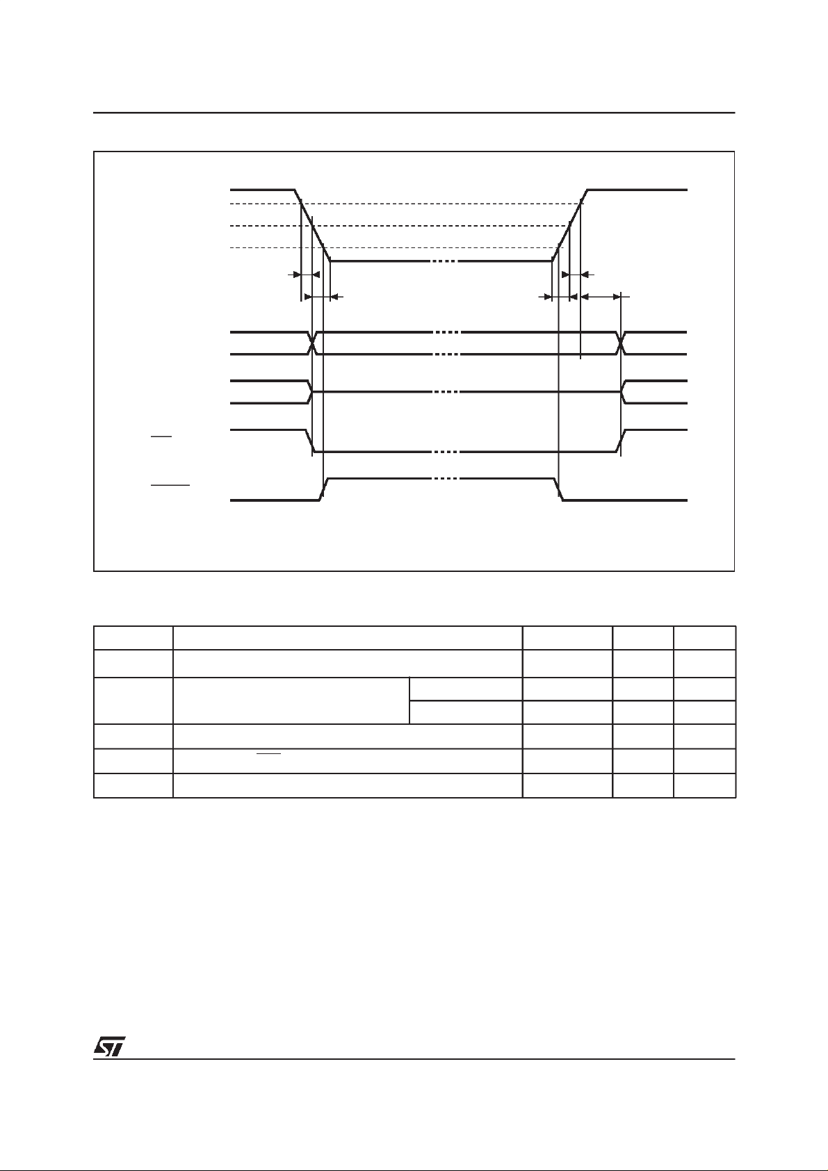
Figure 5. Power Down/Up AC Waveform
V
CC
V
(max)
PFD
V
(min)
PFD
V
SO
tF
tFB
M48T212Y, M48T212V
tR
tRECtRB
INPUTS
OUTPUTS
RST
V
CCSW
VALID VALID
VALID VALID
DON’T CARE
HIGH-Z
AI02638
Table 8. Power Down/Up AC Characteristics
(TA= 0 to70°C)
Symbol Parameter Min Max Unit
V
t
t
FB
t
t
REC
t
RB
(max) to V
F
R
PFD
V
(min) to VSSVCCFallTime
PFD
V
(min) to V
PFD
V
(max) to RST High 40 200 ms
PFD
VSSto V
PFD
(min) VCCFall Time
PFD
(max) VCCRise Time
PFD
(min) VCCRise Time
300 µs
M48T212Y 10 µs
M48T212V 150 µs
10 µs
1 µs
7/23
 Loading...