

SGS Thomson Microelectronics M48T201Y-70MH1, M48T201Y, M48T201V Datasheet
3.3V-5V TIMEKEEPERCONTROLLER
■ CONVERTS LOW POWER SRAMs into
NVRAMs
■ YEAR 2000 COMPLIANT
■ BATTERY LOW FLAG
■ INTEGRATED REAL TIME CLOCK,
POWER-FAIL CONTROL CIRCUIT,
BATTERY and CRYSTAL
■ WATCHDOG TIMER
■ WRITE PROTECT VOLTAGES
(V
= Power-fail Deselect Voltage):
PFD
– M48T201Y: 4.1V ≤ V
– M48T201V: 2.7V ≤ V
■ PACKAGING INCLUDESa44-LEADSOIC and
SNAPHATTOP
(to beOrdered Separately)
■ SOIC PACKAGE PROVIDES DIRECT
CONNECTION for a SNAPHAT TOP which
CONTAINS the BATTERY and CRYSTAL
■ MICROPROCESSOR POWER-ON RESET
(Valid even during battery back-up mode)
■ PROGRAMMABLE ALARM OUTPUT ACTIVE
IN THE BATTERY BACKED-UP MODE
PFD
PFD
≤ 4.5V
≤ 3.0V
SNAPHAT (SH)
Battery/Crystal
44
1
SOH44 (MH)
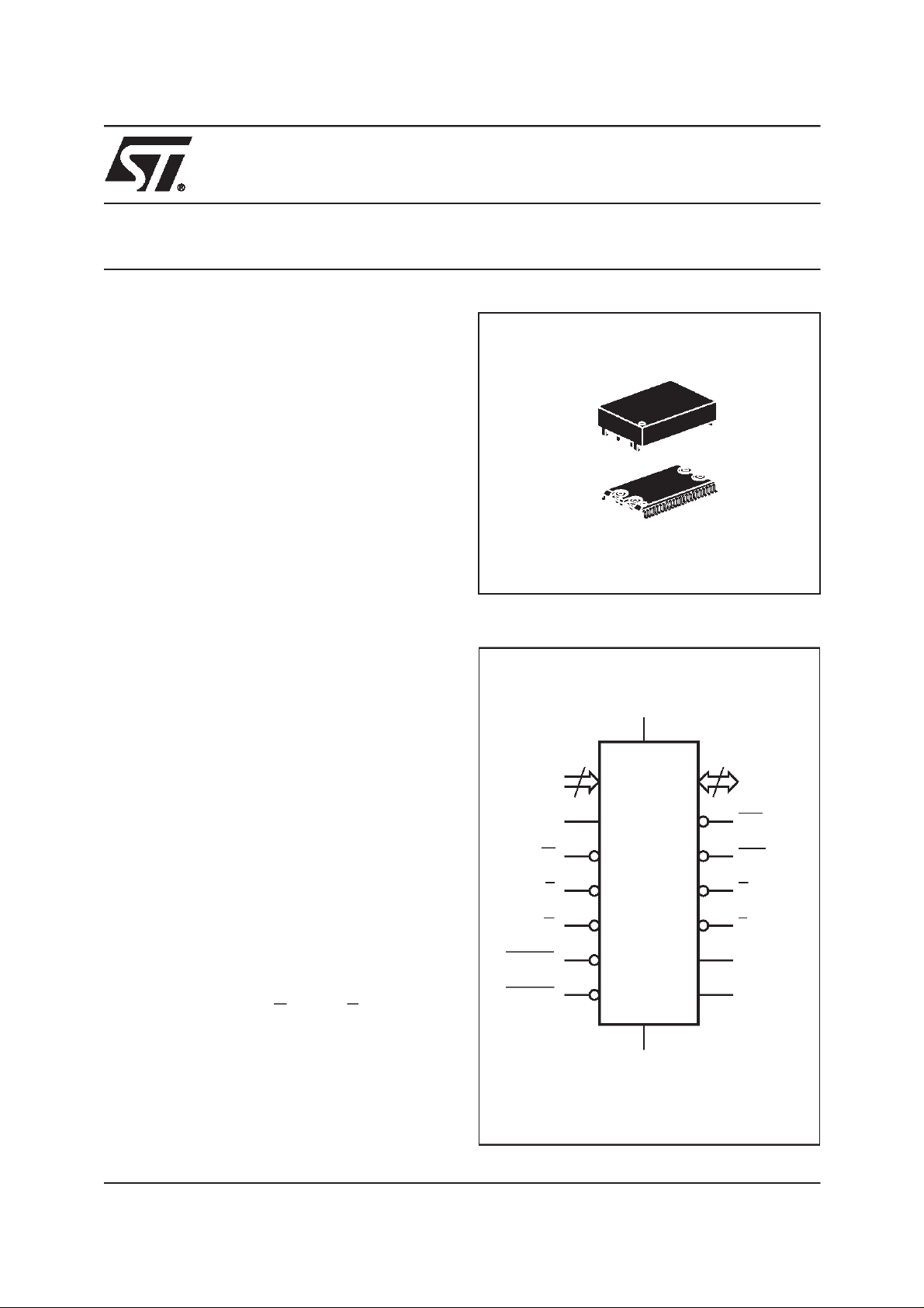
Figure 1. Logic Diagram
V
CC
19
A0-A18
M48T201Y
M48T201V
8
DQ0-DQ7
DESCRIPTION
The M48T201Y/201V are self-contained devices
that include a real time clock (RTC), programmable alarms, a watchdog timer, and a square wave
output which provides control of up to 512K x 8 of
external low-power static RAM. Access to all RTC
functions and the external RAM is the same as
conventional bytewide SRAM. The 16 TIMEKEEPERregisters offer year, month, date, day,
hour, minute, second, calibration, alarm, century,
watchdog, andsquare waveoutput data.Externally attached static RAMs are controlled by the
M48T201Y/201V via the G
CON
and E
CON
signals.
The 44 pin 330mil SOIC provides sockets with
gold plated contacts at both ends for direct connection to a separate SNAPHAT housing containing the battery and crystal. The unique design
allows the SNAPHAT battery package to be
mounted on top of the SOIC package after the
completion of the surface mount process.
WDI
W
RSTIN1
RSTIN2
IRQ/FT
M48T201Y
E
G
M48T201V
V
SS
RST
G
CON
E
CON
SQW
V
OUT
AI02240
1/24November 1999
M48T201Y, M48T201V,
Figure 2. SOIC Connections
RSTIN1
RSTIN2
RST
NC
A18
A16
A14
A12
A7
A6
A5
A4
A3
A2
A1
A0
WDI
G
CON
DQ0
DQ1
DQ2 21
V
SS
1
2
3
4
5
6
7
8
9
10
11
M48T201Y
12
M48T201V
13
14
15
16
17
18
19
20
44
43
42
41
40
39
38
37
36
35
34
33
32
31
30
29
28
27
26
25
24
2322
AI02241
V
CC
V
OUT
SQW
IRQ/FT
A17
A15
A13
A8
A9
A11
G
W
NC
A10
E
E
CON
DQ7
DQ6
DQ5
DQ4
DQ3
NC
Table 1. Signal Names
A0-A18 Address Inputs
DQ0-DQ7 Data Inputs / Outputs
RSTIN1 Reset 1 Input
RSTIN2 Reset 2 Input
RST Reset Output (Open Drain)
WDI Watchdog Input
E Chip Enable Input
G Output Enable Input
W Write Enable Input
E
CON
G
CON
IRQ/FT
SQW
V
OUT
V
CC
V
SS
RAM Chip Enable Output
RAM Enable Output
Interrupt / Frequency Test Output
(Open Drain)
Square Wave Output
Supply Voltage Output
Supply Voltage
Ground
Insertion of the SNAPHAT housing after reflow
prevents potential battery damage due to the high
temperatures required for device surface-mounting. TheSNAPHAT housing iskeyedto preventreverse insertion. The SOIC and battery packages
are shipped separately in plastic anti-static tubes
or in Tape & Reel form. For the 44 lead SOIC, the
battery/crystal package (i.e. SNAPHAT) part number is ”M4Txx-BR12SH1” (See Table 14).
Caution: Do not place the SANPHAT battery/crystal top in conductive foam,as this will drain the lithium button-cell battery.
Automatic backup and write protection for an external SRAMis provided through V
G
pins. (Users are urged to insurethat voltage
CON
OUT,ECON
, and
specifications, for both the controller chip and external SRAM chosen, are similar.) The SNAPHAT
containing the lithium energy source used to permanently power the real time clock is also used to
retain RAM data in the absence of VCCpower
2/24
NC Not Connected Internally
through the V
RAM (E
(G
CON
) andthe output enableoutput to RAM
CON
) are controlled during power transients to
pin. The chip enable output to
OUT
prevent data corruption. The date is automatically
adjusted for months with less than 31 days and
corrects for leap years. The internal watchdog timer provides programmable alarm windows.
The nine clock bytes (7FFFFh-7FFF9h and
7FFF1h) are not the actual clock counters, they
are memory locations consisting of BiPORT
read/write memory cells within the static RAM array. Clock circuitry updates the clock bytes with
current informationonce per second. The information canbe accessedby theuser inthe same manner as any other location in the static memory
array. Byte 7FFF8h is the clock control register.
This byte controls user access to the clock information and also stores the clock calibration setting.
M48T201Y, M48T201V,
Table 2. Absolute Maximum Ratings
(1)
Symbol Parameter Value Unit
T
A
T
STG
T
SLD
V
IO
V
CC
I
O
P
D
Note: 1. Stresses greater than those listed under ”Absolute Maximum Ratings” may cause permanent damage to thedevice. This is a stress
2. Soldering temperature not to exceed 260°C for 10 seconds (total thermal budget not to exceed 150°C for longer than 30 seconds).
CAUTION: Negative undershoots below –0.3V are not allowed on any pin while in the Battery Back-up mode.
CAUTION: Do NOT wave solder SOIC to avoiddamaging SNAPHATsockets.
Table 3. Operating Modes
Mode
Deselect
Write
Read
Read
Deselect
Deselect
Note: 1. X = VIHor VIL.
2. V
Ambient Operating Temperature 0 to 70 °C
Storage Temperature (VCCOff,Oscillator Off)
(2)
Lead Solder Temperature for 10 seconds 260 °C
Input or Output Voltages
Supply Voltage
SNAPHAT –40 to 85 °C
SOIC –55 to 125 °C
–0.3 to V
CC
+0.3
V
M48T201Y –0.3 to 7.0 V
M48T201V –0.3 to 4.6 V
Output Current 20 mA
Power Dissipation 1 W
rating only and functional operation of the device at these or any other conditions above those indicated in the operational section
of this specification is not implied. Exposure to the absolute maximum rating conditions for extended periods of time may affect
reliability.
(1)
V
CC
4.5V to 5.5V
or
3.0V to 3.6V
to V
V
SO
PFD
≤ V
SO
= Battery Back-up Switchover Voltage. (See Tables 6A and 6B for details).
SO
(min)
(2)
(2)
E G W DQ0-DQ7 Power
V
IH
V
IL
V
IL
V
IL
X X High Z Standby
X
V
IL
V
IH
V
IL
V
IH
V
IH
D
D
OUT
IN
Active
Active
High Z Active
X X X High Z CMOS Standby
X X X High Z Battery Back-up Mode
Byte 7FFF7h contains the watchdog timer setting.
The watchdog timer can generate either a reset or
an interrupt, depending on the state of the Watchdog Steering bit (WDS). Bytes 7FFF6h - 7FFF2h
include bits that, when programmed, provide for
clock alarm functionality. Alarms are activated
when the register content matches the month,
date, hours, minutes, and seconds of the clock
registers. Byte 7FFF1h contains century information. Byte7FFF0h containsadditionalflag information pertaining to the watchdog timer, the alarm
condition, the battery statusand square wave output operation. 4-bits are included within this regis-
ter (RS0-RS3) that are used to program the
Square Wave Output Frequency (see Table 11).
The M48T201Y/V also has its own Power-Fail Detect circuit. This control circuitry constantly monitors the supply voltage for an out of tolerance
condition. When VCCis out of tolerance,the circuit
write protects the TIMEKEEPER register data and
external SRAM, providing data security in the
midst of unpredictable system operation. As V
CC
falls, the control circuitry automatically switchesto
the battery, maintaining data and clock operation
until valid power is restored.
3/24
M48T201Y, M48T201V,
Figure 3. Block Diagram
0.1µF
5V
32,768
Hz
CRYSTAL
LITHIUM
CELL
M48T201Y/V
V
CC
E
W
G
WDI
RSTIN1
RSTIN2
V
SS
A0-A18
IRQ/FT
DQ0-DQ7
V
OUT
ECON
GCON
RST
SQW
0.1µF
V
E
W
G
V
A0-Axx
CC
CMOS
SRAM
SS
DQ0-DQ7
AI00604
Figure 4. AC Testing Load Circuit
DEVICE
UNDER
TEST
CLincludes JIG capacitance
Note: Excluding open-drain output pin.
4/24
645Ω
CL= 100pF
1.75V
AI02330
Table 4. AC Measurement Conditions
Input Rise and Fall Times ≤ 5ns
Input Pulse Voltages 0 to 3V
Input and Output Timing Ref.Voltages 1.5V
Note that Output Hi-Z is defined asthe point wheredata isnolonger
driven.
Address Decoding
The M48T201Y/V accommodates 19 address
lines (A0-A18) which allow direct connection of up
to 512K bytesof static RAM. Regardless of SRAM
density used, timekeeping, watchdog, alarm, century, flag, and control registers are located in the
upper RAM locations. All TIMEKEEPER registers
reside in the upper RAM locations without conflict
by inhibiting the G
(output enable RAM) signal
CON
during clock access. TheRAM’s physical locations
are transparent to the user and the memory map
looks continuousfrom thefirst clock address to the
upper most attached RAM addresses.
M48T201Y, M48T201V,
Table 5. Capacitance
(1)
(TA=25°C, f = MHz)
Symbol Parameter Test Condition Min Max Unit
C
IN
C
IO
Note: 1. Effective capacitance measured with power supply at 5V. Sampled only, not 100% tested.
2. Outputs deselected.
Input Capacitance
(2)
Input / Output Capacitance
V
V
OUT
IN
=0V
=0V
10 pF
10 pF
Table 6A. DC Characteristics
(TA= 0 to 70 °C; VCC= 3.0V to 3.6V)
Symbol Parameter Test Condition Typ Min Max Unit
(1, 2)
I
LI
I
LO
I
I
I
Input Leakage Current 0V ≤ VIN≤ V
(1)
Output Leakage Current
I
Supply Current Outputs open 4 10 mA
CC
Supply Current (Standby) TTL
CC1
Supply Current (Standby) CMOS
CC2
Battery Current OSC ON 575 800 nA
BAT
Battery Current OSC OFF 100 nA
V
Input Low Voltage –0.3 0.8 V
IL
V
Input High Voltage 2.0
IH
Output Low Voltage IOL= 2.1mA 0.4 V
V
OL
Output Low Voltage (open drain)
V
V
OHB
I
OUT1
I
OUT2VOUT
V
V
V
Note: 1. Outputs deselected.
Output High Voltage
OH
(4)
VOH(Battery Back-Up) I
(5)
V
Current (Active) V
OUT
Current (Battery Back-Up) V
Power Fail Deselect 2.9 2.7 3.0 V
PFD
Battery Back-Up Switchover
SO
Battery Voltage 3.0 V
BAT
2. RSTIN1 andRSTIN2 internally pulled-up to V
3. For IRQ/FT, RST pins (Open Drain).
4. Conditioned outputs (E
Higher leakage currents will reduce battery life.
5. External SRAM must match TIMEKEEPER Controller chip V
CON
and G
(3)
) can only sustain CMOS leakage current in the battery back-up mode.
CON
CC
0V ≤ V
E=V
OUT
E=V
CC
≤ V
IH
–0.2V
CC
IOL= 10.0mA
I
= –1.0mA
OH
= –1.0µA
OUT2
OUT1>VCC
OUT2>VBAT
–0.3
–0.3 100 µA
V
–
PFD
2.4 V
2.0 3.6 V
100mV
through 100KΩ resistor. WDI internally pulled-down to VSSthrough 100KΩ resistor.
CC
specification.
CC
±1 µA
±1 µA
3mA
2mA
V
+ 0.3
CC
0.4 V
70 mA
V
V
5/24
M48T201Y, M48T201V,
Table 6B. DC Characteristics
(TA= 0 to 70 °C; VCC= 4.5V to 5.5V)
Symbol Parameter Test Condition Typ Min Max Unit
(1, 2)
I
LI
I
LO
I
I
I
Input Leakage Current
(1)
Output Leakage Current
I
Supply Current Outputs open 8 15 mA
CC
Supply Current (Standby) TTL
CC1
Supply Current (Standby) CMOS
CC2
Battery Current OSC ON 575 800 nA
BAT
Battery Current OSC OFF 100 nA
V
Input Low Voltage –0.3 0.8 V
IL
V
Input High Voltage 2.2
IH
Output Low Voltage
V
OL
Output Low Voltage (open drain)
V
V
OHB
I
OUT1
I
OUT2VOUT
V
V
V
Note: 1. Outputs deselected.
Output High Voltage
OH
(4)
VOH(Battery Back-Up) I
(5)
V
Current (Active) V
OUT
Current (Battery Back-Up) V
Power Fail Deselect 4.35 4.1 4.5 V
PFD
Battery Back-Up Switchover 3.0 V
SO
Battery Voltage 3.0 V
BAT
2. RSTIN1 andRSTIN2 internally pulled-up to V
3. For IRQ/FT, RST pins (Open Drain).
4. Conditioned outputs (E
Higher leakage currents will reduce battery life.
5. External SRAM must match TIMEKEEPER Controller chip V
CON
and G
) can only sustain CMOS leakage current in the battery back-up mode.
CON
0V ≤ V
0V ≤ V
E=V
(3)
IOL= 10.0mA
I
OUT2
OUT1>VCC
OUT2>VBAT
through 100KΩ resistor. WDI internally pulled-down to VSSthrough 100KΩ resistor.
CC
I
OL
E=V
≤ V
IN
≤ V
OUT
IH
–0.2V
CC
= 2.1mA
CC
CC
±1 µA
±1 µA
5mA
3mA
V
+ 0.3
CC
0.4 V
0.4 V
= –1.0mA
OH
2.4 V
= –1.0µA2.03.6V
–0.3
–0.3
specification.
CC
100 mA
100 µA
V
6/24
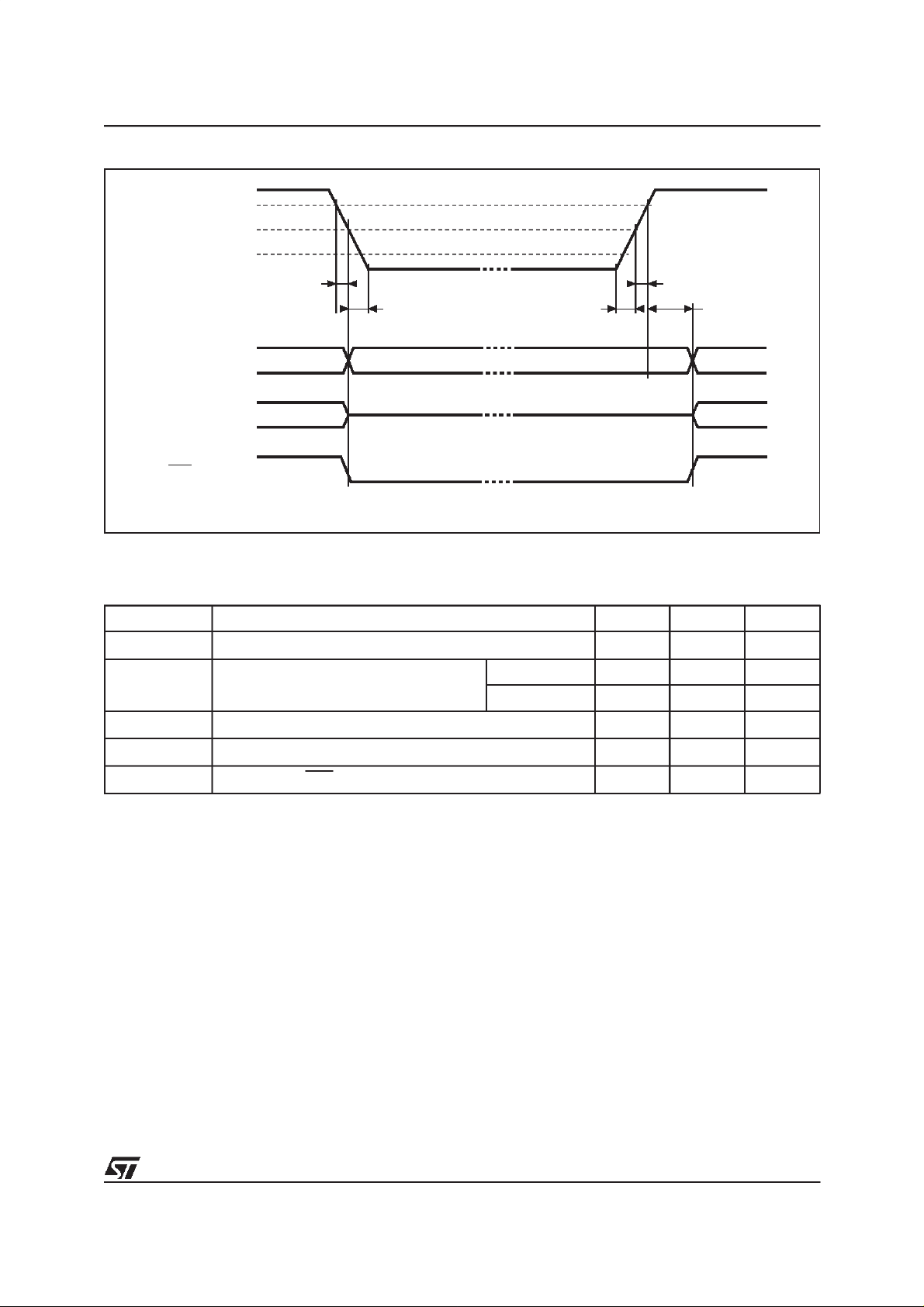
Figure 5. Power Down/Up Mode AC Waveforms
V
CC
V
(max)
PFD
V
(min)
PFD
V
SO
tF
tFB
M48T201Y, M48T201V,
tR
tRECtRB
INPUTS
OUTPUTS
RST
VALID VALID
VALID VALID
Table 7. Power Down/Up Trip Points DC Characteristics
DON’T CARE
HIGH-Z
(1)
(TA= 0 to 70 °C)
Symbol Parameter Min Max Unit
t
t
t
REC
t
FB
t
RB
F
R
V
(max) to V
PFD
V
(min) to VSSVCCFall Time
PFD
V
(min) to V
PFD
VSSto V
V
(max) to RST High
PFD
PFD
PFD
(min) VCCRise Time 5 µs
PFD
(min) VCCFallTime
(max) VCCRise Time
300 µs
M48T201Y 10 µs
M48T201V 150 µs
10 µs
40 200 ms
AI03519
7/24
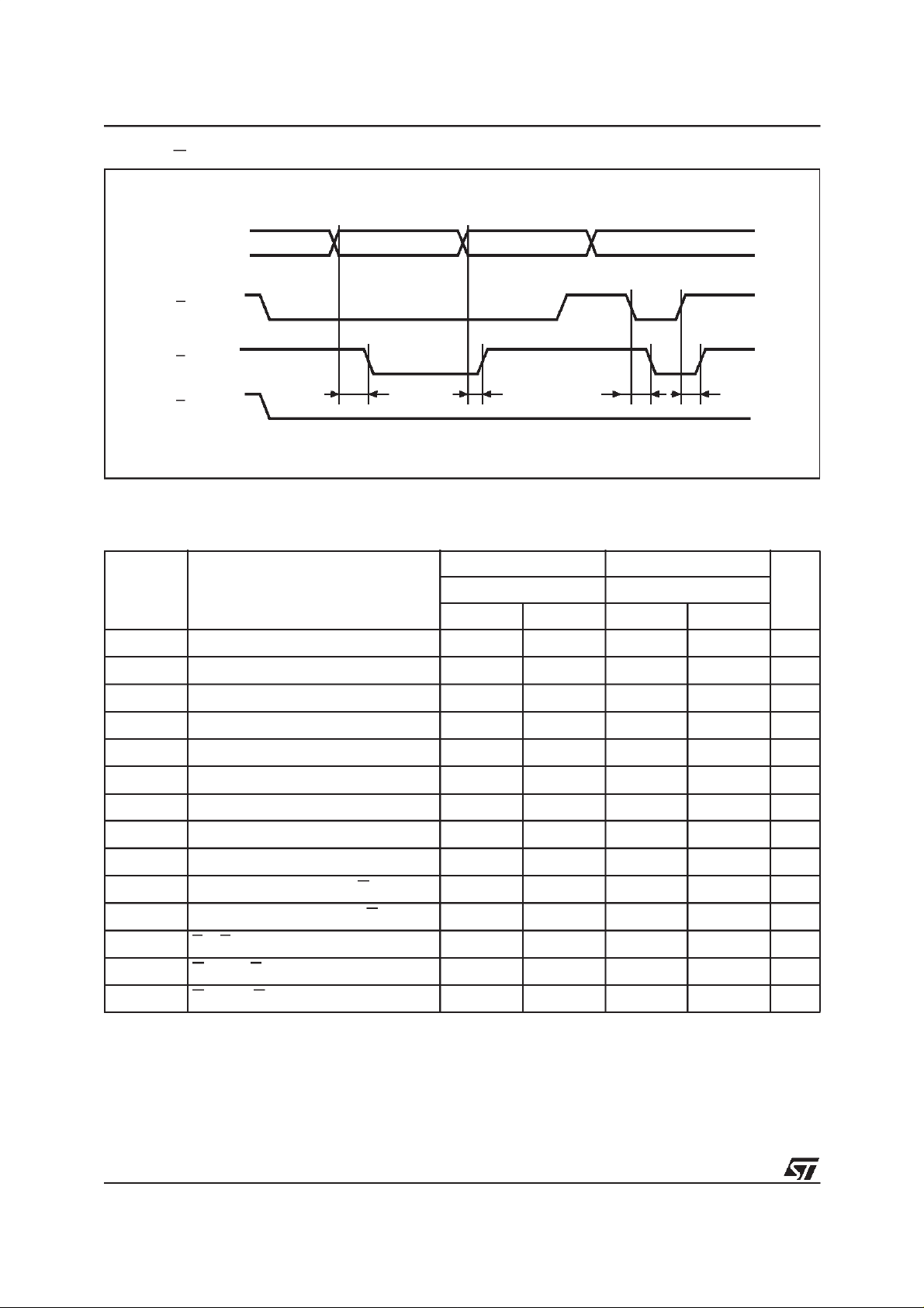
M48T201Y, M48T201V,
Figure 6. G
Timing When Switching Between RTC and External SRAM
CON
ADDRESS
G
G
CON
E
00000h - 7FFEFh 7FFF0h - 7FFFFh 00000h - 7FFEFh7FFF0h - 7FFFFh
Table 8. Read Mode AC Characteristics
(TA= 0 to 70 °C)
Symbol Parameter
tAOEL
tAOEH tOERL tRO
AI02333
M48T201Y M48T201V
Unit-70 -85
Min Max Min Max
t
AVAV
t
AVQV
t
ELQV
t
GLQV
t
ELQX
t
GLQX
t
EHQZ
t
GHQZ
t
AXQX
t
AOEL
t
AOEH
t
EPD
t
OERL
t
RO
Read Cycle Time 70 85 ns
Address Valid to Output Valid 70 85 ns
Chip Enable Low to Output Valid 70 85 ns
Output Enable Low to Output Valid 25 35 ns
Chip Enable Low to Output Transition 5 5 ns
Output Enable Low to Output Transition 0 0 ns
Chip Enable High to Output Hi-Z 20 25 ns
Output Enable High to Output Hi-Z 20 25 ns
Address Transition to Output Transition 5 5 ns
External SRAM Address to G
Controller SRAM Address to G
EtoE
G Low to G
G High to G
Low or High 10 15 ns
CON
Low
CON
High
CON
Low 20 30 ns
CON
CON
High
20 30 ns
15 20 ns
10 15 ns
8/24
 Loading...