

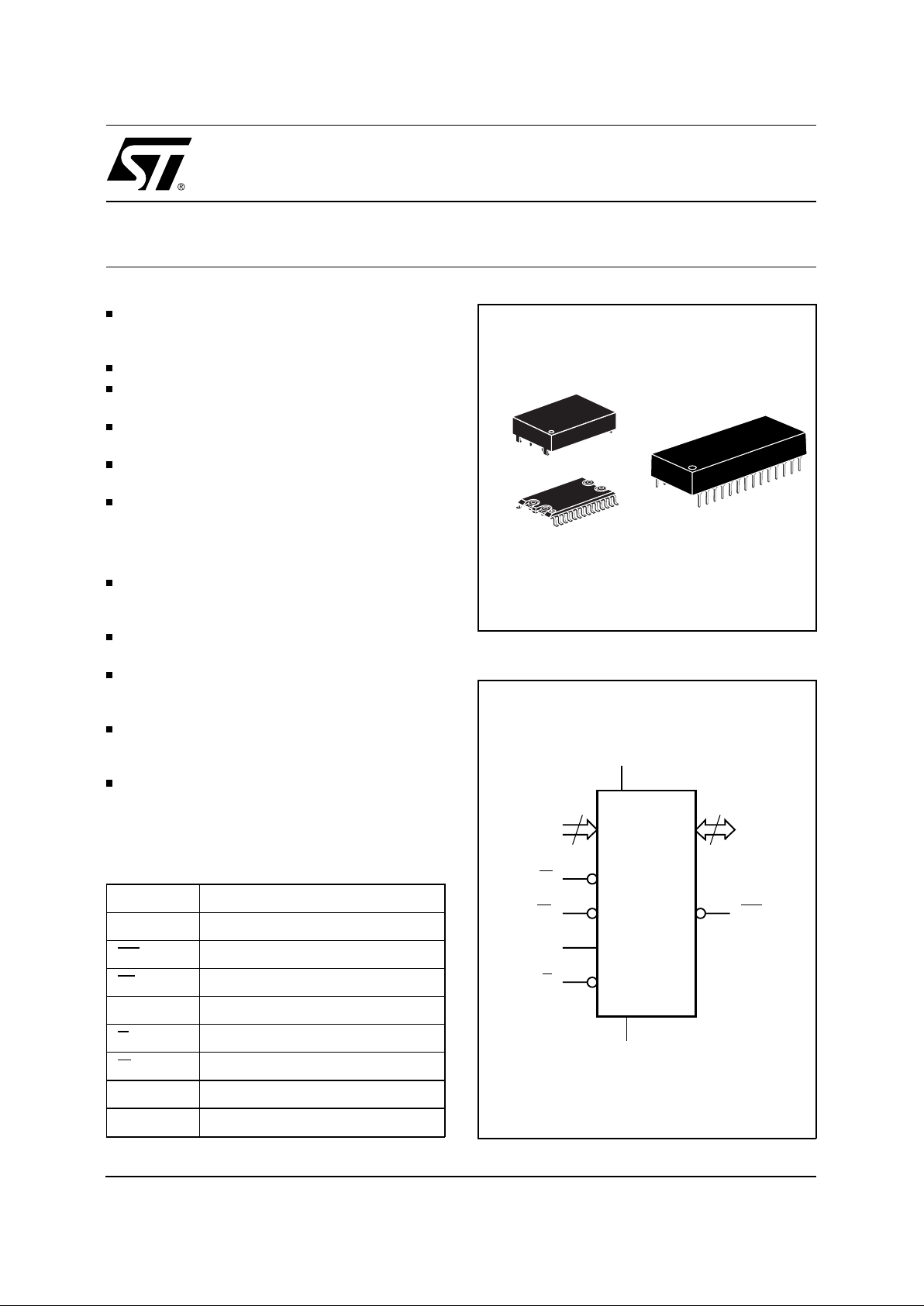
SGS Thomson Microelectronics M48T18-150MH1, M48T18-120MH1, M48T18-100PC1, M48T18, M48T18-150PC1 Datasheet
...
M48T08
M48T18
64 Kbit (8Kb x 8) TIMEKEEPER® SRAM
May 1999 1/19
INTEGRATED ULTRA LOW POWER SRAM,
REAL TIME CLOCK , PO WE R-FAIL C O NTRO L
CIRCUIT and BA T TER Y
BYTEWIDE RAM-LIKE CLOCK ACCE S S
BCD CODED YEAR, MONTH, DAY, DA TE,
HOURS, MINUTES and SECONDS
TYPICAL CLOCK A CCURA CY of ± 1 MINUTE
a MONTH, at 25°C
AUTOMATIC POWER-F AIL CHIP DES ELECT and
WRITE PROTECTION
WRITE PROTECT VOLT AGES
(V
PFD
= Power-fail Deselect Voltage):
– M48T08: 4.5V ≤ V
PFD
≤
4.75V
– M48T18: 4.2V ≤ V
PFD
≤
4.5V
SOFTWARE CONTROLLED CLOCK
CALIBRA TION for HIGH ACCURACY
APPLICATIONS
SELF-CONTAINED BA TTER Y and CRYST AL in the
CAPHA T DIP P ACKAGE
PACKAGING INCLUDES a 28-LEAD SOIC
and SNAPHAT
®
TOP
(to be Ordered Separately)
SOIC PACKAGE PROVIDES DIRECT
CONNECTION for a SNAPHAT TOP which
CONTAINS the BATTERY and CRYSTAL
PIN and FUNCTION COMPATIBLE with
DS1643 and JEDEC STANDARD 8K x 8
SRAMs
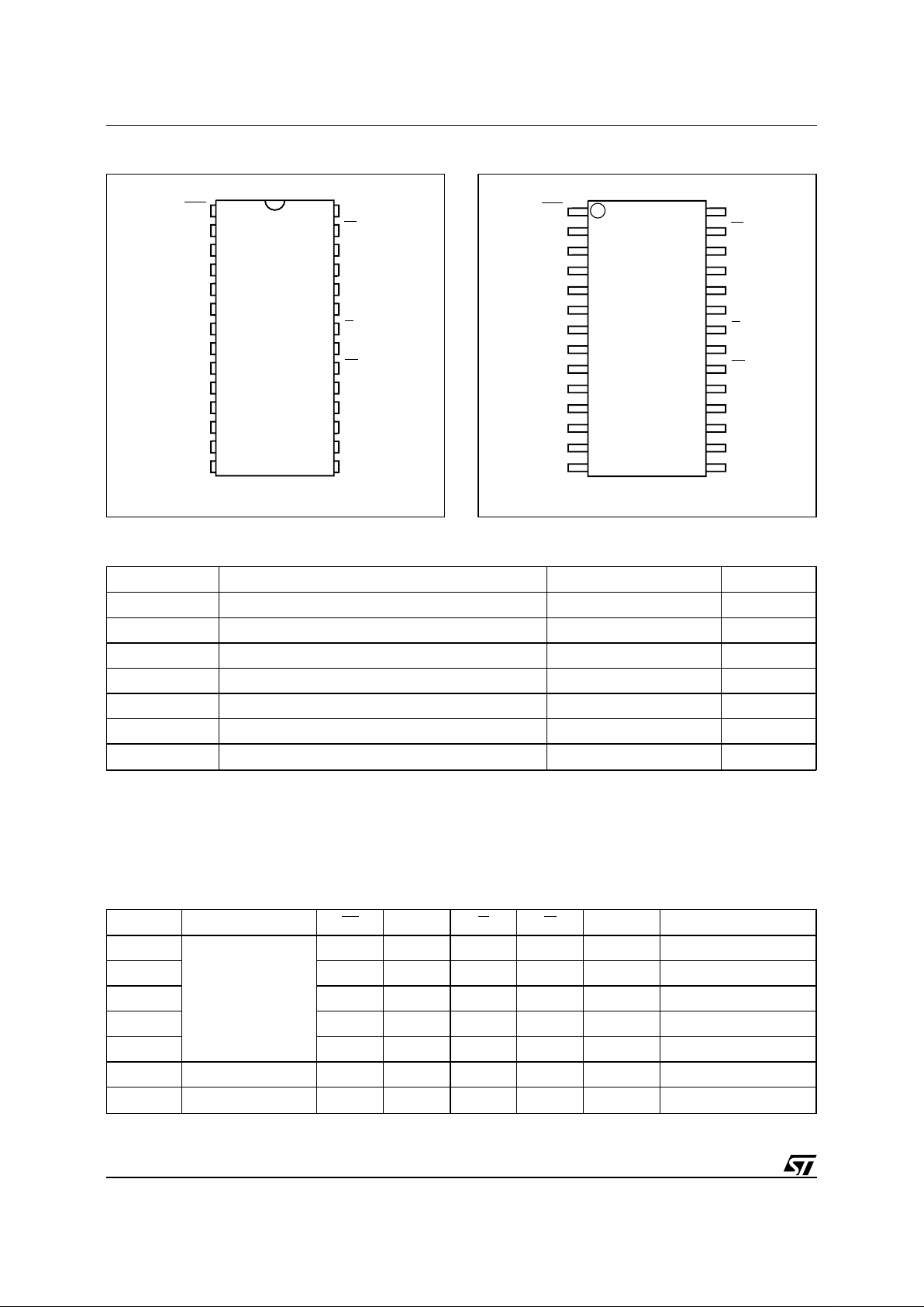
AI01020
13
A0-A12
W
DQ0-DQ7
V
CC
M48T08
M48T18
G
E2
V
SS
8
E1 INT
Figure 1. Logic Diagram
A0-A12 Address Inputs
DQ0-DQ7 Data Inputs / Outputs
INT Power Fail Interrupt (Open Drain)
E1 Chip Enable 1
E2 Chip Enable 2
G Output Enable
W Write Enable
V
CC
Supply Voltage
V
SS
Ground
T ab le 1. Signal Names
28
1
PCDIP28 (PC)
Battery/Crystal
CAPHAT
SNAPHAT (SH)
Battery/Crystal
28
1
SOH28 (MH)
Symbol Parameter Value Unit
T
A
Ambient Operating Temperature 0 to 70 °C
T
STG
Storage T emper ature (VCC Off, Oscillator Off) –40 to 85 °C
T
SLD
(2)
Lead Solder Temperature for 10 seconds 260 °C
V
IO
Input or Output Voltages –0.3 to 7 V
V
CC
Supply Voltage –0.3 to 7 V
I
O
Output Current 20 mA
P
D
Power Dissipation 1 W
Notes:
1. Stresses greater than those listed under "Absolute Maximum Ratings" may cause permanent damage to the device. This is a
stress rating only and functional operation of the device at these or any other conditions above those indi cat ed in the operati onal
section of this specification is not implied. Exposure to the absolute maximum rating conditions for extended periods of time may
affect reliability.
2. Soldering temperature not to exceed 260°C for 10 seconds (total thermal budget not to exceed 150°C for longer than 30 seconds).
CAUTION: Negat i ve undershoots below –0.3 volts are not allowed on any pin while in the Battery Back-up mode.
CAUTION: Do NOT wave solder SOIC to avoid damaging SNAPHAT sockets.
T ab le 2. Absolute Maximum Ratings
(1)
Mode V
CC
E1 E2 G W DQ0-DQ7 Power
Deselect
4.75V to 5.5V
or
4.5V to 5.5V
V
IH
X X X High Z Standby
Deselect X V
IL
X X High Z Standby
Write V
IL
V
IH
XVILD
IN
Active
Read V
IL
V
IH
V
IL
V
IH
D
OUT
Active
Read V
IL
V
IH
V
IH
V
IH
High Z Active
Deselect V
SO
to V
PFD
(min) X X X X High Z CMOS Standby
Deselect ≤ V
SO
X X X X High Z Battery Back-up Mode
Notes:
1. X = V
IH
or VIL; VSO = Battery Back-up Switchover Voltage.
T ab le 3. Operating Modes
A1
A0
DQ0
A7
A4
A3
A2
A6
A5
E2
A10
A8
A9
DQ7
W
A11
G
E1
DQ5DQ1
DQ2
DQ3V
SS
DQ4
DQ6
A12
INT V
CC
AI01182
M48T08
M48T18
8
1
2
3
4
5
6
7
9
10
11
12
13
14
16
15
28
27
26
25
24
23
22
21
20
19
18
17
Figure 2A. DIP Pin Connections
AI01021B
8
2
3
4
5
6
7
9
10
11
12
13
14
22
21
20
19
18
17
16
15
28
27
26
25
24
23
1
A1
A0
DQ0
A7
A4
A3
A2
A6
A5
E2
A10
A8
A9
DQ7
W
A11
G
E1
DQ5DQ1
DQ2
DQ3V
SS
DQ4
DQ6
A12
INT V
CC
M48T18
Figure 2B. SOIC Pin Connections
2/19
M48T08, M48T18
AI01019
5V
OUT
CL = 100pF
CL includes JIG capacitance
1.8kΩ
DEVICE
UNDER
TEST
1kΩ
Figure 4. AC Testing Load Circuit
Input Rise and Fall Times ≤ 5ns
Input Pulse Voltages 0 to 3V
Input and Output Timing Ref. Voltages 1.5V
Note that Output Hi-Z is defined as the point where data is no
longer driven.
T able 4. AC Measurement Conditions
AI01333
LITHIUM
CELL
OSCILLATOR AND
CLOCK CHAIN
V
PFD
INTV
CC
V
SS
32,768 Hz
CRYSTAL
VOLTAGE SENSE
AND
SWITCHING
CIRCUITRY
8 x 8 BiPORT
SRAM ARRAY
8184 x 8
SRAM ARRAY
A0-A12
DQ0-DQ7
E1
E2
W
G
POWER
Figure 3. Block Diagram
DESCRIPTION
The M48T08/18 TIMEKEEPE R
®
RAM is an 8K x 8
non-volatile static RAM and real time clock which
is pin and functional compatible with the DS1643.
The monolithic chip is available in two special
packages to provide a highly integrated battery
backed-up memory and real time clock solution.
The M48T08/18 is a non-volatile pin and function
equivalent to any JEDEC standard 8K x 8 SRAM.
It also easily fits into many ROM, EPROM, and
EEPROM sockets, providing the non-volatility of
PROMs without any requirement for special write
timing or limitations on the number of writes t hat
can be performed.
The 28 pin 600mil DIP CAPHAT houses the
M48T08/18 silicon with a quartz crystal and a long
life lithium button cell in a single package.
The 28 pin 330mil SOIC provides s ockets with gold
plated contacts at both ends for direct connection
to a separate SNAPHAT housing containing the
battery and crystal. The unique design allows the
SNAPHAT bat tery package to be mounted on t op
of the SOIC package after the completion of the
surface mount process. Insertion of the SNAPHAT
housing after reflow prevents potential battery and
crystal damage due to the hig h temperatures required for device surface-mounting. The SNAPHA T
housing is keyed to prevent reverse insertion.
3/19
M48T08, M48T18
Symbol Parameter Test Condition Min Max Unit
I
LI
(1)
Input Leakage Current 0V ≤ VIN ≤ V
CC
±1 µA
I
LO
(1)
Output Leakage Current 0V ≤ V
OUT
≤ V
CC
±5 µA
I
CC
Supply Current Outputs open 80 mA
I
CC1
(2)
Supply Current (Standby) TTL E1 = VIH, E2 = V
IL
3mA
I
CC2
(2)
Supply Current (Standby) CMOS
E1 = VCC – 0.2V,
E2 = V
SS
+ 0.2V
3mA
V
IL
(3)
Input Low Voltage –0.3 0.8 V
V
IH
Input High Voltage 2.2 VCC + 0.3 V
V
OL
Output Low Voltage IOL = 2.1mA 0.4 V
Output Low Voltage (
INT)
(4)
IOL = 0.5mA 0.4 V
V
OH
Output High Voltage IOH = –1mA 2.4 V
Notes:
1. Outputs Deselected.
2. Measured with Control Bits set as follows: R = ’1’; W, ST , FT = ’0’.
3. Negative spikes of –1V allowed for up to 10ns once per Cycle.
4. The
INT pin is Open Drain.
T ab le 6. DC Characteristics
(T
A
= 0 to 70°C; VCC = 4.75V to 5.5V or 4.5V to 5.5V)
Symbol Parameter Test Condition Min Max Unit
C
IN
Input Capacitance VIN = 0V 10 pF
C
IO
(3)
Input / Output Capacitance V
OUT
= 0V 10 pF
Notes:
1. Effective capacitance measured with power supply at 5V .
2. Sampled only, not 100% tested.
3. Outputs deselected.
T ab le 5. Capacitance
(1, 2)
(T
A
= 25 °C, f = 1 MHz )
Symbol Parameter Min Typ Max Unit
V
PFD
Power-fail Deselect Voltage (M48T08) 4.5 4.6 4.75 V
V
PFD
Power-fail Deselect Voltage (M48T18) 4.2 4.3 4.5 V
V
SO
Battery Back-up Switchover Voltage 3.0 V
t
DR
(2)
Expected Data Retention Time 10 YEARS
Notes:
1. All voltages referenced to V
SS
.
2. At 25°C
T able 7. Power Down/Up Trip Points DC Characteristics
(1)
(T
A
= 0 to 70°C)
The SOIC and battery/crystal packages are
shipped separately in plastic anti-static tubes or in
Tape & Reel form. For the 28 lead SOIC, the
battery/crystal package (i.e. SNAPHAT) part number is "M4T28-BR12SH1".
As Figure 3 shows, the static memory array and the
quartz controlled clock oscillator of the M48T08/18
are integrated on one silicon chip. The two circuits
are interconnected at the upper eight memory locations to provide user accessible BYTEWIDE
clock information in the bytes with addresses
1FF8h-1FFFh.
DESCRIPTION
(cont’d)
4/19
M48T08, M48T18
Symbol Parameter Min Max Unit
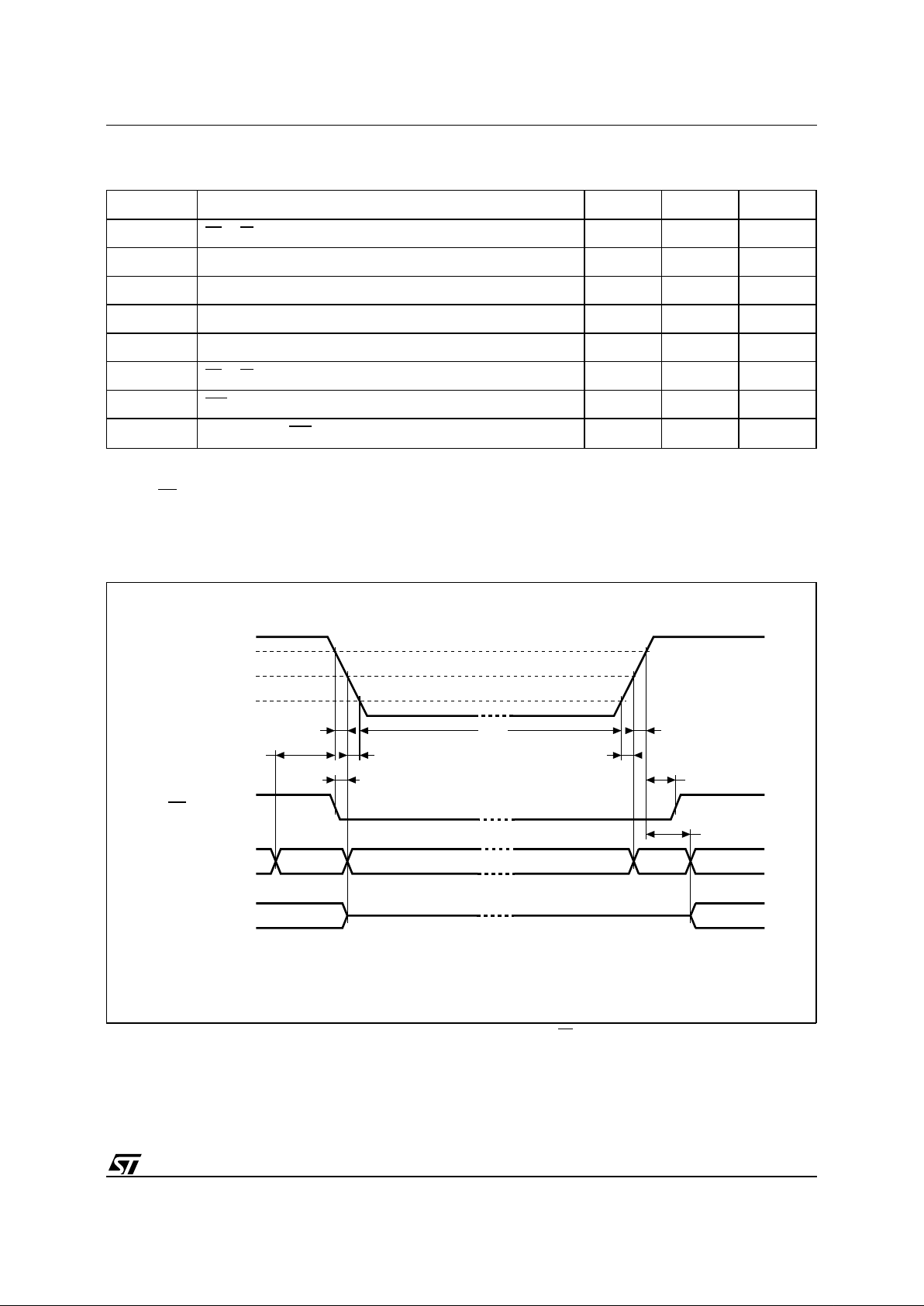
t
PD
E1 or W at VIH or E2 at VIL before Power Down 0 µs
t
F
(1)
V
PFD
(max) to V
PFD
(min) VCC Fall Time 300 µs
t
FB
(2)
V
PFD
(min) to VSO VCC Fall Time 10 µs
t
R
V
PFD
(min) to V
PFD
(max) VCC Rise Time 0 µs
t
RB
VSO to V
PFD
(min) VCC Rise Time 1 µs
t
REC
E1 or W at VIH or E2 at VIL after Power Up 1 ms
t
PFX
INT Low to Auto Deselect 10 40 µs
t
PFH
(3)
V
PFD
(max) to INT High 120 µs
Notes
:1.V
PFD
(max) to V
PFD
(min) fall time of less than tF may result in deselection/writ e protection not occ urri ng until 200 µs after
V
CC
passes V
PFD
(min).
2. V
PFD
(min) to VSO fall time of less than tFB may cause corruption of RAM data.
3.
INT may go high anytime after VCC exceeds V
PFD
(min) and is guaranteed to go high t
PFH
after VCC exceeds V
PFD
(max).
T able 8. Power Down/Up Mode AC Characteristics
(T
A
= 0 to 70°C)
AI00566
V
CC
INPUTS
INT
(PER CONTROL INPUT)
OUTPUTS
DON'T CARE
HIGH-Z
tF
tFB
tPFX
tR
tPFH
tREC
tPD tRB
tDR
VALID VALID
NOTE
(PER CONTROL INPUT)
RECOGNIZEDRECOGNIZED
V
PFD
(max)
V
PFD
(min)
VSO
Figure 5. Power Down/Up Mode AC Waveforms
Note:
Inputs may or may not be recognized at this time. Caution should be taken to keep
E1 high or E2 low as VCC rises past V
PFD
(min).
Some systems may perform inadvertent write cycles after V
CC
rises above V
PFD
(min) but before normal system operations begin. Even
though a power on reset is being applied to the processor, a reset condition may not occur until after the system clock is runn ing.
5/19
M48T08, M48T18
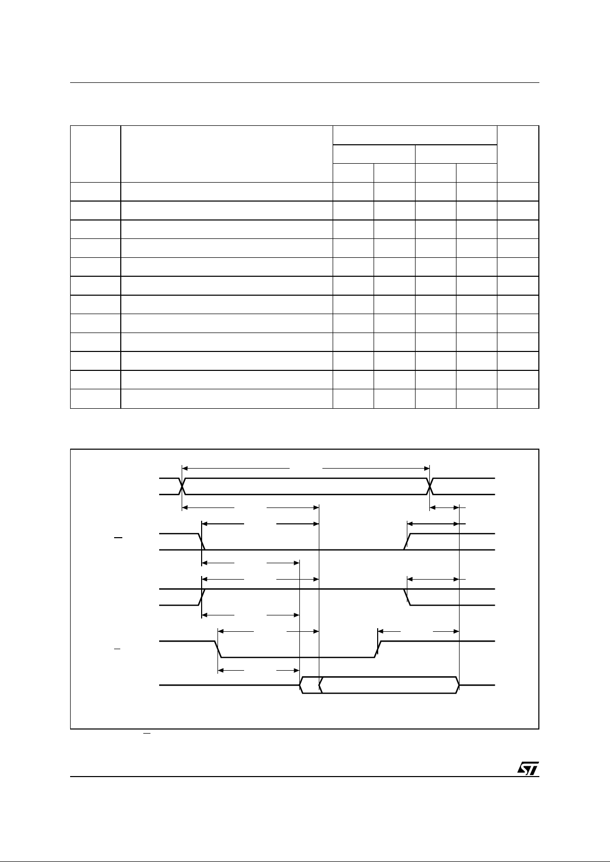
Symbol Parameter
M48T08 / M48T18
Unit
-100 -150
Min Max Min Max
t
AVAV
Read Cycle Time 100 150 ns
t
AVQV
Address Valid to Output Valid 100 150 ns
t
E1LQV
Chip Enable 1 Low to Output Valid 100 150 ns
t
E2HQV
Chip Enable 2 High to Output Valid 100 150 ns
t
GLQV
Output Enable Low to Output Valid 50 75 ns
t
E1LQX
Chip Enable 1 Low to Output Transition 10 10 ns
t
E2HQX
Chip Enable 2 High to Output Transition 10 10 ns
t
GLQX
Output Enable Low to Output Transition 5 5 ns
t
E1HQZ
Chip Enable 1 High to Output Hi-Z 50 75 ns
t
E2LQZ
Chip Enable 2 Low to Output Hi-Z 50 75 ns
t
GHQZ
Output Enable High to Output Hi-Z 40 60 ns
t
AXQX
Address Transition to Output Transition 5 5 ns
T ab le 9. Read Mode AC Characteristics
(T
A
= 0 to 70°C; VCC = 4.75V to 5.5V or 4.5V to 5.5V)
AI00962
tAVAV
tAVQV tAXQX
tE1LQV
tE1LQX
tE1HQZ
tGLQV
tGLQX
tGHQZ
VALID
A0-A12
E1
G
DQ0-DQ7
tE2HQV
tE2HQX
VALID
tE2LQZ
E2
Figure 6. Read Mode AC Waveforms
Note:
Write Enable (
W) = High.
6/19
M48T08, M48T18
 Loading...