

SGS Thomson Microelectronics M29F040 Datasheet
M29F040
4 Mbit (512Kb x8, Uniform Block) Singl e Supply Flash Memory
NOT FOR NEW DESIGN
M29F040 is replaced by the M29F040B
5V ± 10% SUPPLY VOLTAGE for PROGRAM ,
ERASE and READ OPERATIONS
FA ST A CCE SS TI ME: 70ns
BYTE PROGRAMMING TIME: 10µs typical
ERASE TIME
– Block: 1.0 sec typical
– Chip: 2.5 sec typical
PROGRAM/ERASE CONTROLLER (P/E.C.)
– Program Byte-by-Byte
– Data Polling and Toggle bits Protocol for
P/E.C. Stat us
MEMORY ERASE in BLOCKS
– 8 Uniform Blocks of 64 KBytes each
– Block Protection
– Multiblock Erase
ERASE SUSPEND and RESUME MODES
LOW POWER CONSUMP TION
– Read mode: 8mA typical (at 12MHz)
– Stand-by mode: 25µA typical
– Automatic Stand-by mode
100,000 PROGRAM/ERASE CYCLES per
BLOCK
20 YEARS DAT A RETENTION
– Defectivity below 1ppm/year
ELECTRONIC SIGNATURE
– Manufacturer Code: 20h
– Device Code: E2h
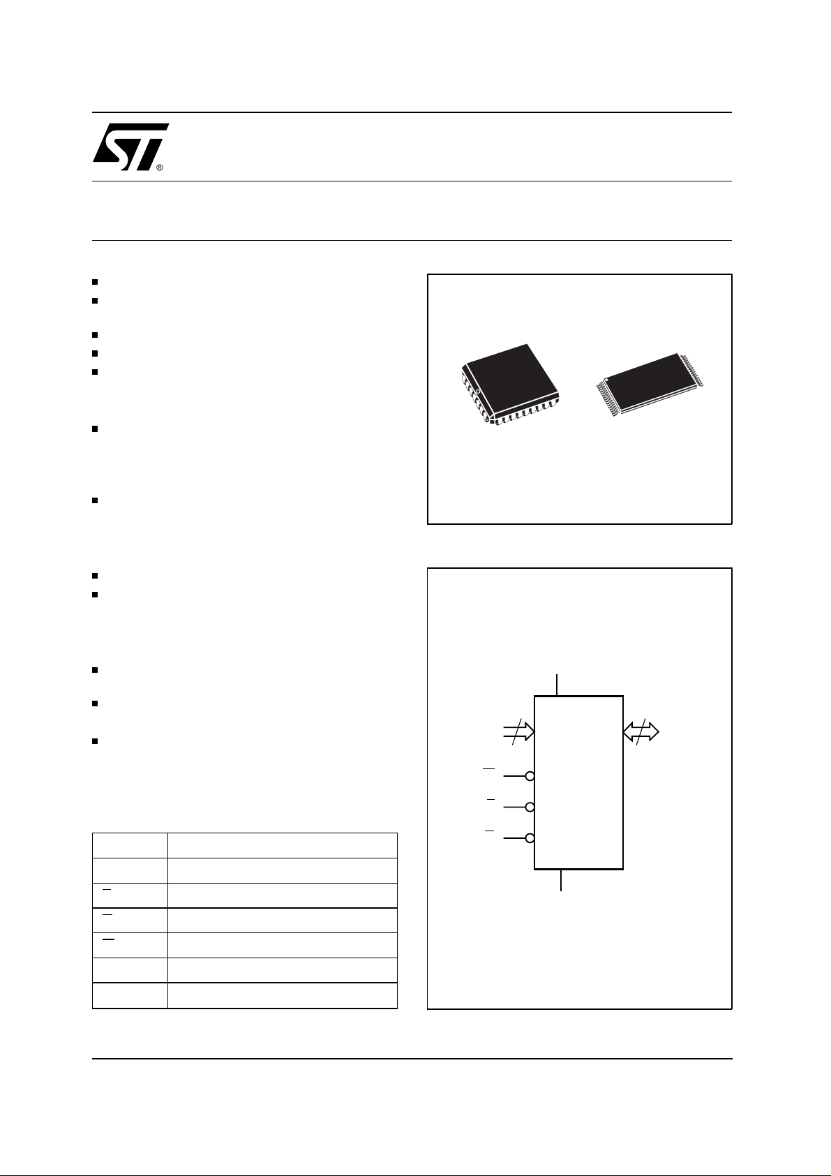
Figure 1. Logic Diagram
PLCC32 (K) TSOP32 (N)
V
CC
19
A0-A18
W
M29F040
8 x 20 mm
8
DQ0-DQ7
Table 1. Signal Names
E
A0-A18 Address Inputs
DQ0-DQ7 Data Input / Outputs
E Chip Enable
G Output Enable
W Write Enable
V
CC
V
SS
November 1999 1/31
This is information on a product still in production but not recommended for new designs.
Supply Voltage
Ground
G
V
SS
AI01372
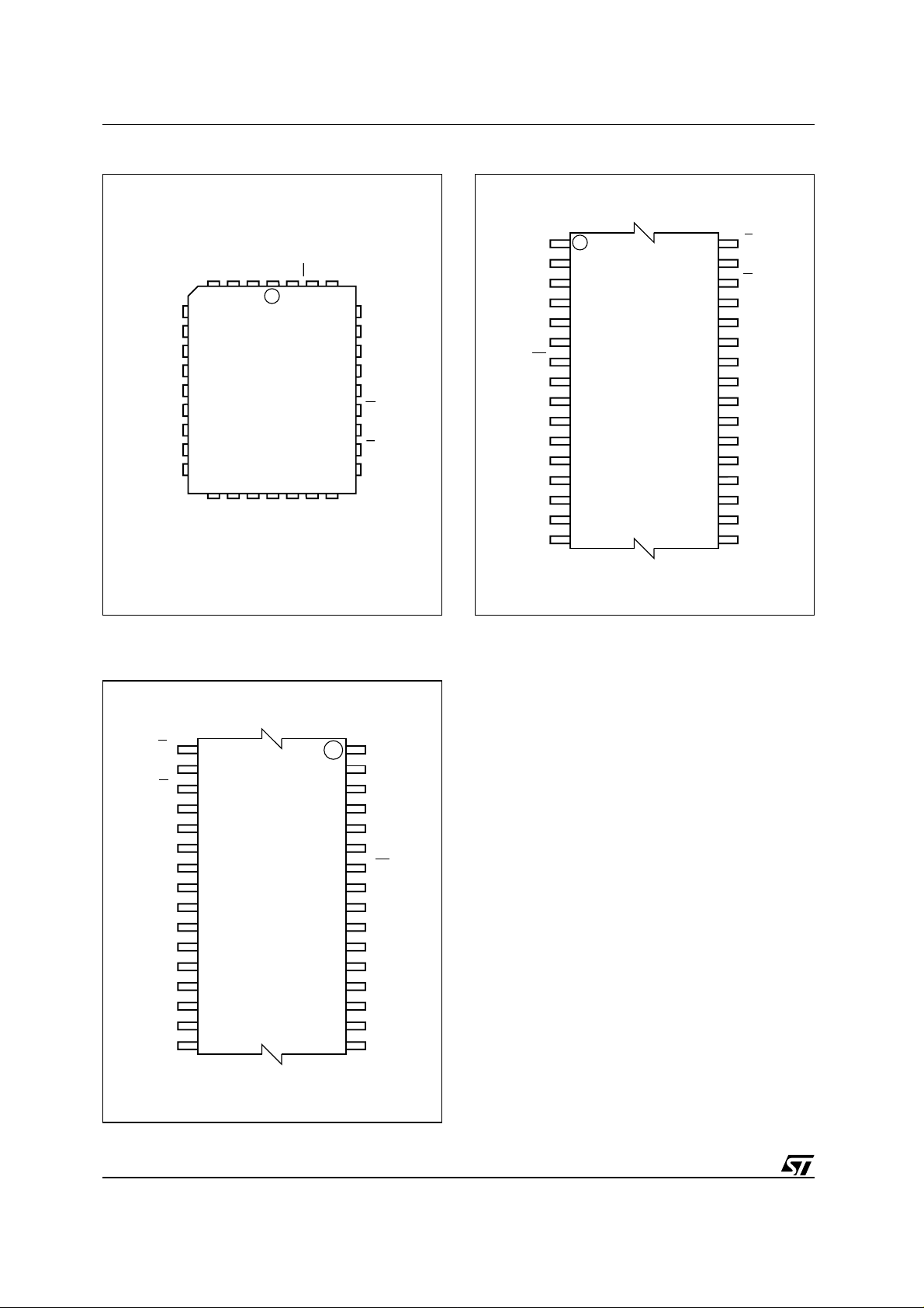
M29F040
Figure 2A. LCC Pin Connections
CC
A18
32
DQ3
V
DQ4
W
DQ5
A7
A6
A5
A4
A3
A2
A1
A0
DQ0
A16
A12
A15
1
DQ1
DQ2
M29F040
17
SS
V
9
A17
25
DQ6
A14
A13
A8
A9
A11
G
A10
E
DQ7
AI01378
Figure 2B. TSOP Pin Connections
A11 G
A13
A14
A17
V
CC
A18
A16
A15
A12
1
A9
A8
W
8
M29F040
(Normal)
9
A7
A6
A5
16 17
A4 A3
32
25
24
AI01379
A10
E
DQ7
DQ6
DQ5
DQ4
DQ3
V
SS
DQ2
DQ1
DQ0
A0
A1
A2
Figure 2C. TSOP Reverse Pin Connections
A11G
A9
A8
A13
A14
A17
W
V
CC
A18
A16
A15
A12
A7
A6
A5
A4A3
A10
DQ7
DQ6
DQ5
DQ4
DQ3
V
SS
DQ2
DQ1
DQ0
A0
A1
A2
1
E
8
9
16 17
M29F040
(Reverse)
32
25
24
AI01174B
DESCRIPTION
The M29F040 is a non-volatile memory that may
be erased electrically at the block level, and programmed Byte-by-Byte.
The interface is directly compatible with most microprocessors. PLCC32 and TSOP32 (8 x 20mm)
packages are available. Both normal and reverse
pin outs are available for the TSOP32 package.
Organisation
The Flash Memory organisation is 512K x8 bits with
Address lines A0-A18 and Data Inputs/Outputs
DQ0-DQ7. Memory control is provided by Chip
Enable, Output Enable and Write Enable Inputs.
Erase and Program are performed through the
internal Program/Erase Controller (P/E.C.).
Data Outputs bits DQ7 and DQ6 provide polling or
toggle signals during Automatic Program or Erase
to indicate the Ready/Busy state of the internal
Program/Erase Controller.
Memory Blocks
Erasure of the memory is in blocks. There are 8
uniform blocks of 64 Kbytes each in the memory
address space. Each block can be programmed
and erased over 100,000 cycles. Each uniform
block may separately be protected and unpro-
2/31
M29F040
Table 2. Absolute Maximum Ratings
Symbol Parameter Value Unit
T
A
T
BIAS
T
STG
(2)
V
IO
V
CC
(2)
V
A9
Notes:
1. Except for the rating "Operating Temperature Range", stresses above those listed in the Table "Absolute Maximum Ratings"
may cause permanent damage to the device. These are stress ratings only and operation of the device at these or any other
conditions above those indicated in the Operating sections of this specification is not implied. Exposure to Absolute Maximum
Rating conditions for extended periods may affect device reliability. Refer also to t he STM icro e lect ronics SURE Program and other
relevant quality documents.
2. Minimum Voltage may undershoot to –2V during transition and for less than 20ns.
3. Depends on range.
Ambient Operating Temperature
Temperature Under Bias –50 to 125
Storage Temperature –65 to 150
Input or Output Voltages –0.6 to 7 V
Supply Voltage –0.6 to 7 V
A9 Voltage –0.6 to 13.5 V
tected against program and erase. Block erasure
may be suspended, while data is read from other
blocks of the memory, and then resumed.
Bus Operations
Seven operations can be performed by the appropriate bus cycles, Read Array, Read Electronic
Signature, Output Disable, Standby , P rotect Block,
Unprotect Block, and Write the Command of an
Instruction.
Command Interface
Command Bytes can be written to a Command
Interface (C.I.) latch to perform Reading (from the
Array or Electronic Signature), Erasure or Programming. For added da ta protection, command
execution starts after 4 or 6 command cycles. The
first, second, fourth and fifth cycles are used to
input a code sequence to the Command Inter face
(C.I.). This sequence is equal for all P/E.C. instructions. Command itself and its confirmation - if it
applies - are given on the third and fourth or sixth
cycles.
Instructions
Seven instructions are defined to perform Reset,
Read Electronic Signature, Auto Program, Block
Auto Erase, Chip Auto Erase, Block Erase S uspend
and Block Erase Resume. The internal Program/Erase Controller (P/E.C.) handles all timing
and verification of the Program and Erase instruc-
(1)
(3)
–40 to 125
tions and provides Data Polling, T oggle, and Status
data to indicate completion of Program and Erase
Operations.
Instructions are composed of up to six cycles. The
first two cycles input a code sequence to the Command Interface which is common to all P/E.C.
instructions (see Table 7 for Command Descriptions). The third cycle inputs the instruction set up
command instruction to the Command Interface.
Subsequent cycles output Signature, Block Protection or the addressed data for Read operations.
For added data protection, the instructions for program, and block or chip erase require further command inputs. For a Program instruction, the fourth
command cycle inputs the address and data to be
programmed. For an Erase instruction (block or
chip), the fourth and fifth cycles input a further code
sequence before the Erase confirm command on
the sixth cycle. Byte programming t akes typically
10µs while erase is performed in typically 1.0 second.
Erasure of a memory block may be suspended, in
order to read data from another block, and then
resumed. Data Polling, Toggle and Error data may
be read at any time, including during the programming or erase cycles, to monitor the progress of
the operation. When power is first applied or if V
falls below V
, the command interface is reset to
LKO
Read Array.
C
°
C
°
C
°
CC
3/31
M29F040
Table 3. Operations
Operation E G W DQ0 - DQ7
Read V
Write V
Output Disable V
Standby V
Note:
X = V
IL
or V
IH
Table 4. Electronic Signature
IL
IL
IL
IH
V
IL
V
IH
V
IH
X X Hi-Z
V
IH
V
IL
V
IH
Data Output
Data Input
Hi-Z
Code E G WA0A1A6A9
Manufact. Code V
Device Code V
V
IL
V
IL
V
IL
IL
IH
V
IH
V
IL
V
IH
V
IL
V
IL
V
IL
V
IL
Table 5. Block Protection Status
Code E G W A0 A1 A6 A16 A17 A18
Protected Block V
Unprotected Block V
Note:
SA = Address of block being checked
DEVICE OPERATION
Signal Descriptions
Address Inputs (A0-A18).
the memory array are latched during a write operation. The A9 address input is used also for the
Electronic Signature read and Block Protect verification. When A9 is raised to V
Manufacturer Code, Read Device Code or Verify
Block Protection is enabled depending on the com bination of levels on A0, A1 and A6. When A0, A1
and A6 are Low, the Electronic Signature Manufacturer code is read, when A0 is High and A1 and A6
are Low, the Device code is read, and when A1 is
High and A0 and A6 ar e low, the Block Protection
Status is read for the block addressed by A16, A17,
A18.
Data Input/Outputs (DQ0-DQ7).
a byte to be programmed or a command written to
the C.I. Both are latched when Chip Enable
Write Enable
W are active. The data output is from
the memory Array, the Electronic Signature, the
Data Polling bit (DQ7), t he Toggle Bit (DQ6), the
Error bit (DQ5) or the Erase Timer bit (DQ3). Ouputs are valid when Chip Enable
Enable
G are active. The output is high impedance
V
IL
IL
V
IL
IH
V
V
IL
IH
The address inputs for
, either a Read
ID
The data input is
E and Output
V
V
IL
IL
V
IH
V
IH
E and
V
SA SA SA Don’t Care 01h
IL
V
SA SA SA Don’t Care 00h
IL
when the chip is deselected or the outputs are
disabled.
Chip Enable (
memory control logic, input buffers, decoders and
sense amplifiers.
reduces the power consumption to the standby
E can also be used to control writing to the
level.
command register and to the memory array, while
W remains at a low level. Addresses are then
latched on the falling edge of
on the rising edge of
forced to V
Output Enable (
outputs through the data buffers during a read
operation.
Block Protect and Block Unprotect operations.
Write Enable (
Command Register and Address and Data latches.
Addresses are latched on the falling edge of
Data Inputs are latched on the rising edge of
Supply Voltage.
V
CC
operations (Read, Program and Erase).
Ground.
V
SS
measurements.
Other
Addresses
V
V
E).
ID
ID
Don’t Care 20h
Don’t Care E2h
Other
Addresses
The Chip Enable activates the
DQ0 - DQ7
DQ0 - DQ7
E High deselects the memory and
E while data is latched
E. The Chip Enable must be
during Block Unprotect operations.
ID
The Output Enable gates the
G).
G must be forced to VID level during
This input controls writing to the
W).
W, and
W.
The power supply for all
is the reference for all voltage
V
SS
4/31
M29F040
Table 6. Instructions
(1,2)
Mne. Instr. Cyc. 1st Cyc. 2nd Cyc. 3rd Cyc. 4th Cyc. 5th Cyc. 6th Cyc. 7th Cyc.
(3,7)
RST
RSIG
(4)
Reset
Read
Electronic
Read Array/
(4,10)
Signature
RBP
Protection
Read Block
(4)
PG Program 4
BE Block Erase 6
1+
3+
3+
3+
Addr.
Data
Addr.
Data
Addr.
Data
Addr.
Data
Addr.
Data
Addr.
(3,7)
(3,7)
(3,7)
(3,7)
(3,7)
X
Read Memory Array until a new write cycle is initiated.
F0h
5555h 2AAAh 5555h
Read Memory Array until a new write
cycle is initiated.
AAh 55h F0h
5555h 2AAAh 5555h
Read Electronic Signature until a new
write cycle is initiated. See Note 5.
AAh 55h 90h
5555h 2AAAh 5555h
Read Block Protection until a new write
cycle is initiated. See Note 6.
AAh 55h 90h
5555h 2AAAh 5555h
Program
Address
Read Data Polling or Toggle Bit
until Program completes.
AAh 55h A0h
Program
Data
5555h 2AAAh 5555h 5555h 2AAAh
Block
Address
Additional
Block
(8)
Data
Addr.
CE Chip Erase 6
Data
Addr.
ES
Erase
Suspend
1
Data
Addr.
ER
Erase
Resume
1
Data
Notes:
1. Command not interpreted in this table will default to read array mode.
2. While writing any command or duri ng RS G and RSP execution, the P/E.C. can be reset by writing the command 00h to the C.I.
3. X = Don’t Care.
4. The first cycle of the RST, RBP or RSIG instruction is followed by read operations to read memory array, Status Register or
Electronic Signature codes. Any number of read cycles can occur after one command cycle.
5. Signature Address bits A0, A1, A6 at V
Device code.
6. Protection Address: A0, A6 at V
status.
7. Address bits A15-A18 are don’t care for coded address inputs.
8. Optional, additional blocks addresses must be entered within a 80µs delay after last write entry, timeout status can be verified
through DQ3 value. When full command is entered, read Data Polling or Toggle bit until Erase is completed or suspended.
9. Read Data Polling or Toggle bit until Erase completes.
10. A wait time of 5µs is necessary after a Reset command, if the memory is in a Block Erase status, before starting
any operation.
, A1 at VIH and A16, A17, A18 within the uniform block to be checked, will output the Block Protection
IL
AAh 55h 80h AAh 55h 30h 30h
(3,7)
5555h 2AAAh 5555h 5555h 2AAAh 5555h
AAh 55h 80h AAh 55h 10h
(3,7)
X
Read until Toggle stops, then read all the data needed from any
uniform block(s) not being erased then Resume Erase.
B0h
(3,7)
X
Read Data Polling or Toggle Bit until Erase completes or Erase
is suspended another time
30h
will output Manufacturer code (20h). Address bits A0 at VIH and A1, A6 at VIL will output
IL
Note 9
5/31

M29F040
Memory Blocks
The memory blocks of the M29F040 are shown in
Figure 3. The memory array is divided in 8 uniform
blocks of 64 Kbytes. Each block can be erased
separately or any combination of blocks can be
erased simultaneously. The Block Erase operation
is managed automatically by the P/E.C. The operation can be suspended in order to read from any
other block, and then resumed.
Block Protection provides additional data security.
Each uniform block can be separately protected or
unprotected against Program or Erase. Bringing A9
G to VID initiates protection, while bringing A9,
and
G and E to VID cancels the protection. T he block
affected during protection is addressed by the inputs on A16, A17, and A18. Unprotect operation
affects all blocks.
Operations
Operations are defined as specific bus cycles and
signals which allow Memory Read, Command
Write, Output Disable, Standby, Read Status Bits,
Block Protect/Unprotect, Block Protection Check
and Electronic Signature Read. They are shown in
Tables 3, 4, 5.
Read.
Read operations are used to output the
contents of the Memory Array, the Status Register
or the Electronic Signature. Both Chip Enable
and Output Enable
G must be low in order to read
the output of the memory. The Chip Enable input
also provides power control and should be us ed for
device selection. Output Enable should be used to
gate data onto the output independent of the device
selection. The data read depends on the previous
command written to the memory (see instructions
RST and RSIG, and Status Bits).
Write operations are used to give Instruction
Write.
Commands to the memory or to latch input data to
be programmed. A write operation is initiated when
Chip Enable
with Output Enable
on the falling edge of
E is Low and Write Enable W is Low
G High. Addresses are latched
W or E whichever occurs last.
Commands and Input Data are latched on the rising
edge of
Output Disable.
ance when the Output Enable
Enable
Standby.
Enable
W or E whichever occurs first.
The data outputs are high imped-
G is High with Write
W High.
The memory is in standby when Chip
E is High and Program/Erase Controller
P/E.C. is Idle. The power consumption is reduced
to the standby level and the outputs are high impedance, independent of the Output Enable
Write Enable
Automatic Standby.
W inputs.
After 150ns of inactivity and
G or
when CMOS levels are driving the addresses, the
chip automatically enters a pseudo standby mode
where consumption is reduced to the CMOS
standby value, while outputs are still driving the
bus.
Electronic Signature.
Two codes identifying the
manufacturer and the device can be read from the
memory, the manufacturer’s code for STMicroelectronics is 20h, and t he device c ode is E2h for the
M29F040. These codes allow programming equipment or applications to automatically match their
interface to the characteristics of the particular
manufacturer’s product. The Electronic Signature
is output by a Read op eration when the voltage
applied to A9 is at V
and address inputs A1 and
ID
A6 are at Low. The manufacturer code is output
when the Address input A0 is Low and the device
code when this input is High. Other Address inputs
are ignored. The codes are output on DQ0-DQ7.
This is shown in Table 4.
The Electronic Signature can also be read, without
raising A9 to V
by giving the memory the instruc-
ID
tion RSIG (see below).
Block Protection.
Each uniform block can be
separately protected against Program or Erase.
Block Protection provides additional data security,
as it disables all program or erase operations. This
mode is activated when both A9 and
V
and the block address is applied on A16-A18.
E
ID
Block Protection is programmed using a Presto F
program like algorithm. Protection is initiated on the
edge of
the edge of
W falling to VIL. Then after a delay of 100µs,
W rising to VIH ends the protection
operation. Protection verify is achieved by bringing
G, E and A6 to VIL while W is at VIH and A9 at VID.
Under these conditions, reading the data output will
yield 01h if the block defined by the inputs on
A16-A18 is protected. Any att empt to program or
erase a protected block will be ignored by the
device.
Any protected block can be unprotected to allow
updating of bit contents. All blocks must be protected before an unprotect operation. Block Unprotect is activated when A9,
G and E are at VID.
The addresses inputs A6, A12, A16 must be maintained at V
. Block Unprotect is performed through
IH
a Presto F Erase like algorithm. Unprotect is initiated by the edge of
of 10ms, the edge of
W falling to VIL. After a delay
W rising to VIH will end the
unprotection operation. Unprotect verify is
achieved by bringing
G and E to VIL while A6 and
W are at VIH and A9 at VID. In these conditions,
reading the output data will yield 00h if the block
defined by the inputs on A16-A18 has been successfully unprotected. All combinations of A16A18 must be addressed in order to ensure that all
of the 8 uniform blocks have been unprotected.
Block Protection Status is shown in Table 5.
G are set to
6/31
Figure 3. Memory Map and Block Address Table
M29F040
A18
AI01362B
A17
1
1 64K Bytes Block
1
1
0
0
001
000
A16
1
1
0
0
1
1
1
0
1
0
1
0
Instructions and Commands
The Command Interface ( C.I .) latches commands
written to the memory. Instructions are made up
from one or more commands to perform Read
Array/Reset, Read Electronic Signature, Block
Erase, Chip Erase, Program, Block Erase Suspend
and Erase Resume. Commands are made of address and data sequences. Addresses are latched
on the falling edge of
on the rising of
W or E. The instructions require from
W or E and data is latched
1 to 6 cycles, the fi rst or first three of which are
always write operations used to initiate the command. They are followed by either further write
cycles to confirm the first command or execute the
command immediately. Command sequencing
must be followed exactly. Any invalid combination
of commands will reset the device to Read Array.
The increased number of cycles has been chosen
to assure maximum data security. Commands are
initialised by two preceding coded cycles which
unlock the Command Interface. In addition, for
Erase, command confirmation is again preceeded
by the two coded cycles.
P/E.C. status is indicated during command execution by Data Polling on DQ7, detection of Toggle on
64K Bytes Block
64K Bytes Block
64K Bytes Block
64K Bytes Block
TOP
ADDRESS
7FFFFh
6FFFFh
5FFFFh
4FFFFh
3FFFFh
2FFFFh
1FFFFh
0FFFFh
BOTTOM
ADDRESS
70000h
60000h
50000h
40000h
30000h
20000h
10000h
00000h
T ab le 7. Commands
Hex Code Command
00h Read
10h Chip Erase Confirm
30h Block Erase Resume/Confirm
80h Set-up Erase
90h
Read Electronic Signature/
Block Protection Status
A0h Program
B0h Erase Suspend
F0h Read Array/Reset
DQ6, or Error on DQ5 and Erase Timer DQ3 bits.
Any read attempt during Program or Erase command execution will automatically output those four
bits. The P/E.C. automatically sets bits DQ3, DQ5,
DQ6 and DQ7. Other bits (DQ0, DQ1, DQ2 and
DQ4) are reserved for future use and should be
masked.
7/31
M29F040
Table 8. Status Register
DQ Name Logic Level Definition Note
’1’ Erase Complete
Data
7
Polling
’0’ Erase on Going
DQ Program Complete
DQ Program on Going
Indicates the P/E.C. status, check during
Program or Erase, and on completion
before checking bits DQ5 for Program or
Erase Success.
’-1-0-1-0-1-0-1-’ Erase or Program on Going Successive read output complementary
6 Toggle Bit
5 Error Bit
4
Erase
3
Time Bit
2 Reserved
1 Reserved
0 Reserved
Note:
Logic level ’1’ is High, ’0’ is Low. -0-1-0-0-0-1-1-1-0- represent bit value in successive Read operations.
’-0-0-0-0-0-0-0-’
’-1-1-1-1-1-1-1-’
Data Po ll ing b it (DQ7 ).
’1’ Program or Erase Error
’0’ Program or Erase on Going
’1’
’0’
’1’ Erase Timeout Period Expired P/E.C. Erase operation has started. Only
’0’
When Programming op-
Program (’0’ on DQ6)
Complete
Erase or Program
(’1’ on DQ6) Complete
Erase Timeout Period on
Going
erations are in pr ogress, this bit outputs t he complement of the bit being programmed on DQ7.
During Erase operation, it outputs a ’0’. After completion of the operation, DQ7 will output the bit last
programmed or a ’1’ after erasing. Data Polling is
valid only effective during P/E.C. operation, that is
after the fourth
the sixth
W pulse for programming or after
W pulse for Erase. It must be performed
at the address being programmed or at an address
within the block being erased. If the byte to be
programmed belongs to a protected block the command is ignored. If all the blocks selected for erasure are protected, DQ7 will set to ’0’ for about
100µs, and then return to previous addressed
memory data. See Figure 9 for the Data Polling
flowchart and Figure 10 for the Data Polling waveforms.
Toggle bit (DQ6).
When Programming operations
are in progress, successive attempts to read DQ6
will output complementary data. DQ6 will toggle
following toggling of either
G or E when G is low.
data on DQ6 while Programming or Erase
operations are going on. DQ6 remain at
constant level when P/E.C. operations are
completed or Erase Suspend is
acknowledged.
This bit is set to ’1’ if P/E.C. has exceded
the specified time limits.
possible command entry is Erase Suspend
(ES). An additional block to be erased in
parallel can be entered to the P/E.C.
The operation is completed when two successive
reads yield the same output data. The next read
will output the bit las t programmed or a ’1’ after
erasing. The toggle bit is valid only effective during
P/E.C. operations, that is after the fourth
for programming or after the sixth
W pulse
W pulse for
Erase. If the byte to be programmed belongs to a
protected block the command will be ignored. If the
blocks selected for erasure are protected, DQ6 will
toggle for about 100µs and then return back to
Read. See Figure 11 for Toggle Bit flowchart and
Figure 12 for Toggle Bit waveforms.
Error bit (DQ5).
This bit is set to ’1’ by the P/E.C
when there is a failure of byte programming, block
erase, or chip erase that results in invalid data
being programmed in the memory block. In case of
error in block erase or byte program, the block in
which the error occured or to which the programmed byte belongs, must be discarded. Other
blocks may still be used. Error bit resets after Reset
(RST) instruction. In case of success, the error bit
will set to ’0’ during Program or Erase and to valid
data after write operation is completed.
8/31
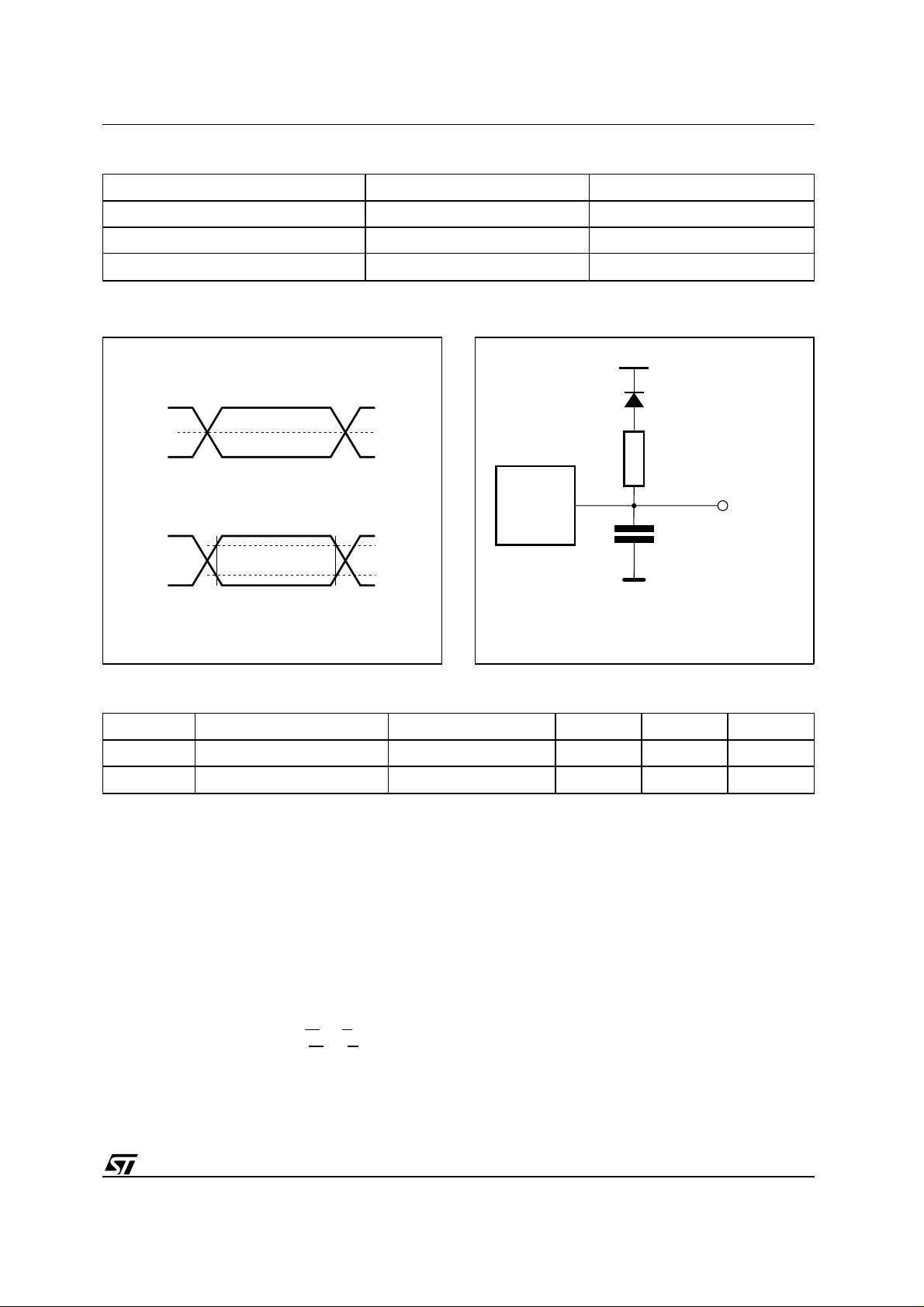
Table 9. AC Measurement Conditions
High Speed Standard
Input Rise and Fall Times
Input Pulse Voltages 0 to 3V 0.45V to 2.4V
Input and Output Timing Ref. Voltages 1.5V 0.8V and 2V
10ns
≤
10ns
≤
M29F040
Figure 4. AC Testing Input Output Waveform
High Speed
3V
1.5V
0V
Standard
2.4V
0.45V
(1)
Table 10. Capacitance
Symbol Parameter Test Condition Min Max Unit
C
IN
C
OUT
Note:
1. Sampled only, not 100% tested.
Input Capacitance VIN = 0V 6 pF
Output Capacitance V
(TA = 25 °C, f = 1 MHz )
2.0V
0.8V
AI01275B
Figure 5. AC Testing Load Circuit
1.3V
1N914
3.3kΩ
DEVICE
UNDER
TEST
C
L
CL = 30pF for High Speed
CL = 100pF for Standard
CL includes JIG capacitance
= 0V 12 pF
OUT
OUT
AI01276B
Erase Timer bit (DQ3).
This bit is set to ’0’ by the
P/E.C. when the last Block Erase command has
been entered to t he Command Interface and it is
awaiting the Erase start. When the wait period is
finished, after 80 to 120µs, DQ3 returns back to ’1’.
Coded Cycles.
The two coded cycles unlock the
Command Interface. They are f ollowed by a c ommand input or a comand confirmation. The coded
cycles consist of writing the data AAh at address
5555h during the first cycle and data 55h at address
2AAAh during the second cycle. Addresses are
latched on the falling edge of
latched on the rising edge of
W or E while data is
W or E. The coded
cycles happen on first and second cycles of the
command write or on the fourth and fifth cycles.
Read Array/Reset (RST) instruction.
The Reset
instruction consists of one write operation gi ving
the command F0h. It can be optionally preceded
by the two coded cycles. A wait state of 5µs before
read operations is necessary if the Reset command
is applied during an Erase operation.
Read Electronic Signature (RSIG) i nstruction.
This instruction uses the two coded cycles followed
by one write cycle giving the command 90h to
address 5555h for command setup. A subsequent
read will output the manufacturer code, the device
code or the Block Protection status depending on
the levels of A0, A1, A6, A16, A17 and A18. The
manufacturer code, 20h, is output when the addresses lines A0, A1 and A6 are Low, the device
code, E2h is output when A0 is High wit h A1 and
A6 Low.
9/31
M29F040
Table 11. DC Characteristics
(T
= 0 to 70°C, –20 to 85°C, –40 to 85°C or –40 to 125°C; VCC = 5V ± 10%)
A
Symbol Parameter Test Condition Min Max Unit
I
I
LO
I
CC1
I
CC2
I
CC3
I
CC4
Input Leakage Current 0V ≤ VIN ≤ V
LI
Output Leakage Current 0V ≤ V
Supply Current (Read) E = VIL, G = VIH, f = 6MHz 15 mA
Supply Current (Standby) TTL E = V
Supply Current (Standby) CMOS E = VCC ± 0.2V 50
Supply Current (Program or Erase)
Byte Program,
Block Erase
OUT
≤ V
IH
CC
CC
1
±
1
±
1mA
20 mA
A
µ
A
µ
A
µ
I
CC5
V
V
V
V
V
I
V
LKO
Read Block Protection (RBP) instruction.
Supply Current Chip Erase in progress 40 mA
Input Low Voltage –0.5 0.8 V
IL
Input High Voltage 2 VCC + 0.5 V
IH
Output Low Voltage IOL = 10mA 0.45 V
OL
Output High Voltage TTL IOH = –2.5mA 2.4 V
OH
Output High Voltage CMOS
A9 Voltage (Electronic Signature) 11.5 12.5 V
ID
A9 Current (Electronic Signature) A9 = V
ID
Supply Voltage (Erase and
Program lock-out)
The
use of Read Electronic Signature (RSIG) command
also allows access to the Block Protection status
verify. After giving the RSIG command, A0 and A6
are set to V
with A1 at VIH, while A16, A17 and
IL
A18 define the block of the block to be verified. A
read in these conditions will output a 01h if block is
protected and a 00h if block is not protected.
This Read Block Protection is the only valid way to
check the protection statu s of a block. Nevertheless, it must not be used during the Block Protection
phase as a method to verify the block protection.
Please refer to Block Protection paragraph.
Chip Erase (CE) instruction.
This instruction uses
six write cycles. The Erase Set-up command 80h
is written to address 5555h on third cycle after the
two coded cycles. The Chip Erase Conf irm com-
I
= –100µAV
OH
I
= –2.5mA 0.85 V
OH
ID
–0.4 V
CC
CC
50
3.2 4.2 V
mand 10h is written at address 5555h on sixth cycle
after another two coded cycles. If the second command given is not an erase confirm or if the coded
cycles are wrong, the instruction aborts and the
device is reset to Read Array . It is not necess ary to
program the array with 00h f irst as the P/E.C. will
automatically do this before erasing to FFh. Read
operations after the sixth rising edge of
output the status register bits. During the execution of the erase by the P/E.C. the memory accepts
only the Reset (RST) command. Read of Data
Polling bit DQ7 returns ’0’, then ’1’ on completion.
The T oggle Bit DQ6 toggles dur ing erase operation
and stops when erase is completed. After completion the Status Register bit DQ5 returns ’1’ if there
has been an Erase Failure because the erasure
has not been verified even after the maximum
number of erase cycles have been executed.
V
A
µ
W or E
10/31
 Loading...