

SGS Thomson Microelectronics M28W800CT, M28W800CB Datasheet
FEATURES SUMMARY
■ SUPPLY VOLTAGE
–V
–V
–V
■ ACCE SS TIME: 70, 85, 90,10 0ns
■ PROGRAMMING TIME:
= 2.7V to 3.6V Core Power Supply
DD
= 1.65V to 3.6V for Input/Output
DDQ
= 12V for fast Program (optional)
PP
– 10µs typical
– Double Word Programming Option
■ COMMON FLASH INTERFACE
– 64 bit Security Code
■ MEMORY BLOCKS
– Parameter Blocks (Top or Bottom location)
– M ain Blocks
■ BLOCK LOCKING
– All blocks locked at Power Up
– Any combinat ion of blocks can be locked
for Block Lock-Down
–WP
■ SECURITY
– 64 bit user Programmable OT P cells
– 64 bit uniqu e device identifier
– One Parameter Block Permanently Lo ckable
■ AUTOMAT IC S TAND-BY M ODE
■ PROGRAM and ERASE SUSPEND
■ 100,000 PROGRAM/ERASE CYCLES per
BLOCK
■ ELECTRONIC SIGNATURE
– Manufacturer Code: 20h
– Top Device Code, M28W800CT: 88CCh
– Bottom Device Code, M28W800CB: 88CDh
M28W800CT
M28W800CB
8 Mbit (512Kb x16, Boot Block)
3V Supply Flash Memory
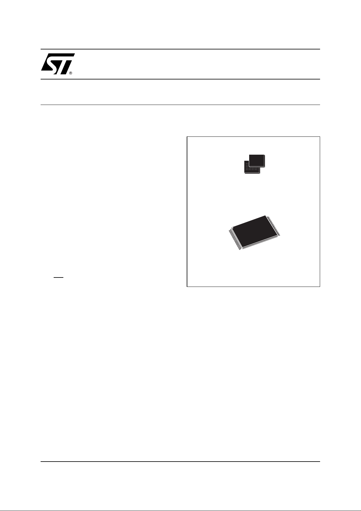
Figure 1. Packages
FBGA
TFBGA46 (ZB)
6.39 x 6.37mm
TSOP48 (N)
12 x 20mm
1/49May 2002

M28W800CT, M28W800CB
TABLE OF CONTENTS
SUMMARYDESCRIPTION...........................................................5
Figure2.LogicDiagram ..........................................................5
Table 1. Signal Nam es . . . ........................................................5
Figure 3. TSOP Connections.......................................................6
Figure 4. TFBGA Connections (Top view through package). ..............................7
Figure5.BlockAddresses.........................................................8
Figure6.SecurityBlockandProtectionRegisterMemoryMap............................8
SIGNALDESCRIPTIONS............................................................9
AddressInputs(A0-A18)..........................................................9
Data Input/Output (DQ0-DQ15). . . ..................................................9
ChipEnable(E). ................................................................9
Output Enabl e (G). ..............................................................9
Write Enable (W). . ..............................................................9
WriteProtect(WP)...............................................................9
Reset(RP).....................................................................9
Supply Voltage..............................................................9
V
DD
V
Supply Voltage.............................................................9
DDQ
ProgramSupplyVoltage ......................................................9
V
PP
V
Ground. ...................................................................9
SS
BUSOPERATIONS................................................................10
Read.........................................................................10
Write.........................................................................10
OutputDisable.................................................................10
Standby. . ....................................................................10
Automatic Standby. .............................................................10
Reset........................................................................10
Read Electroni c Signature Command ...............................................11
Table2.BusOperations.........................................................10
COMMANDINTERFACE ...........................................................11
ReadMemoryArrayCommand....................................................11
ReadStatusRegisterCommand...................................................11
Read Electroni c Signature Command ...............................................11
ReadCFIQueryCommand.......................................................11
BlockEraseCommand..........................................................11
ProgramCommand.............................................................11
Double Word Program Command . .................................................12
ClearStatusRegisterCommand...................................................12
Program/Erase Suspend Command ................................................12
Program/EraseResumeCommand ................................................12
ProtectionRegisterProgramCommand.............................................12
BlockLock-DownCommand......................................................13
2/49

M28W800CT, M28W800CB
Table3.Commands ............................................................14
Table4.ReadElectronicSignature.................................................14
Table 5. Read Block Lock Signature ................................................15
Table6.ReadProtectionRegisterandLockRegister ..................................15
Table7.Program,EraseTimesandProgram/EraseEnduranceCycles ....................15
BLOCKLOCKING.................................................................16
Reading a Block’s Lock Status . . . .................................................16
LockedState..................................................................16
UnlockedState ................................................................16
Lock-DownState...............................................................16
LockingOperationsDuringEraseSuspend ..........................................16
Table8.BlockLockStatus.......................................................17
Table9.ProtectionStatus........................................................17
STATUSREGISTER...............................................................18
Program/EraseControllerStatus(Bit7).............................................18
Erase Suspend Status (Bit 6) .....................................................18
EraseStatus(Bit5).............................................................18
ProgramStatus(Bit4)...........................................................18
Status(Bit3)...............................................................18
V
PP
ProgramSuspendStatus(Bit2)...................................................18
BlockProtectionStatus(Bit1).....................................................19
Reserved(Bit0)................................................................19
Table10.StatusRegisterBits.....................................................19
MAXIMUMRATING................................................................20
Table11.AbsoluteMaximumRatings...............................................20
DCandACPARAMETERS .........................................................21
Table 12. Operating and AC Measurement Conditions..................................21
Figure7.ACMeasurementI/OWaveform ...........................................21
Figure 8. AC Measurement Load Circuit . . . ..........................................21
Table 13. Capacitance...........................................................21
Table14.DCCharacteristics......................................................22
Figure9.ReadModeACWaveforms...............................................23
Table15.ReadACCharacteristics.................................................23
Figure 10. Write AC Waveforms, Write Enable Controlled . . .............................24
Table 16. Write AC Characteristics, Write Enable Co ntrolled .............................25
Figure11.WriteACWaveforms,ChipEnableControlled................................26
Table17.WriteACCharacteristics,ChipEnableControlled .............................27
Figure12.Power-UpandResetACWaveforms.......................................28
Table18.Power-UpandResetACCharacteristics ....................................28
PACKAGE MECHANICAL . . . .......................................................29
3/49

M28W800CT, M28W800CB
Figure13.TSOP48-48leadPlasticThinSmallOutline,12x20mm,PackageOutline ........29
Table 19. TSOP48 - 48 lead Plas tic Thin Small Outline, 12 x 20mm, Package Mechanical Data . 29
Figure 14. TFBGA46 6.39x6.37mm - 8x6 ball array, 0.75mm pitch, Bottom View Package Outline30
Table20.TFBGA466.39x6.37mm-8x6ballarray,0.75mmpitch,PackageMechanicalData...30
Figure 15. TFBGA46 Daisy Chain - Package Connections (Top view through package) ........31
Figure 16. TFBGA46 Daisy Chain - PCB Connections proposal (Top view through package ) ....31
PARTNUMBERING ...............................................................32
Table21.OrderingInformationScheme.............................................32
Table22.DaisyChainOrderingScheme............................................32
REVISIONHISTORY...............................................................33
Table23.DocumentRevisionHistory...............................................33
APPENDIX A. BLOCK ADDRES S T ABLES . . ..........................................34
Table 24. Top Boot Block Addresses, M28W800CT ....................................34
Table25.BottomBootBlockAddresses,M28W800CB.................................34
APPENDIXB.COMMONFLASHINTERFACE(CFI) .....................................35
Table26.QueryStructureOverview................................................35
Table 27. CFI Query Identification String . . ..........................................35
Table28.CFIQuerySystemInterfaceInformation.....................................36
Table29.DeviceGeometryDefinition...............................................37
Table 30. Primary Algorithm-Specific Extended Query Table .............................38
Table31.SecurityCodeArea.....................................................39
APPENDIX C. FLOWCHARTS AND PSEUDO CODES....................................40
Figure 17. Program Flowchart and Pseudo Code. . ....................................40
Figure 18. Double Word Program Flowchart and Pseudo Code ...........................41
Figure 19. Program Suspend & Resum e Flowchart and Pseudo Code .....................42
Figure 20. Erase Flowc hart and Pseudo Code ........................................43
Figure 21. Erase S us pend & Resume Flowchart and Pseudo Code. .......................44
Figure 22. Locking Operations Flowchart and Pseudo Code .............................45
Figure23.ProtectionRegisterProgramFlowchartandPseudoCode......................46
APPENDIXD.COMMANDINTERFACEANDPROGRAM/ERASECONTROLLERSTATE.......47
Table32.WriteStateMachineCurrent/Next,sheet1of2................................47
Table33.WriteStateMachineCurrent/Next,sheet2of2................................48
4/49
SUMMARY DESCRIPTION
The M28W800C isa 8Mbit (512Kbit x16) non-volatileFlashmemorythatcanbeerasedelectrically
at the block level and programmed in-system on a
Word-by-Word basis. These operations can be
performed using a single low voltage (2.7 to 3.6V)
supply. V
1.65V. An optional 12V V
allows to drive the I/O pin down t o
DDQ
power supply is pro-
PP
vided to speed up customer programming.
The device features an asymmetrical blocked ar-
chitecture. The M 28W800C has an array of 23
blocks: 8 Parameter Blocks of 4 KWord and 15
Main Blocks of 32 KWord. M28W800CT has the
Parameter Blocks at the top of the memory address space while the M28W800CB locates the
Parameter Blocks starting from the bottom. The
memory maps are shown in Figure 5, Block Addresses.
The M28W800C features an instant, individual
block locking scheme that allows any block to be
locked or unlocked with no latency, enabling instant code and data protection. All blocks have
three levels of protection. They can be locked and
locked-down individually preventing any accidental programming or erasure. There is an addi tional
hardware protection against program and erase.
When V
PP
≤ V
all blocks are protected against
PPLK
program or erase. All blocks are l oc k ed at powerup.
Each block can be erased separately. Erase can
be suspended in order to perform ei the r read or
program in any other block and then resumed.
Program can be suspended to read data in any
other block and then resumed. Each block can be
programmed and erased over 100,000 cy cles.
The device includ es a 128 bit Protection Register
and a Security Block to increase the protection of
a system desi gn. The Protection Register is divided into two 64 bit segments, the first one contains
a unique device number writte n by ST, while the
second one is one-time-programmable by the user. The user programmable segment can be permanently protected. The Security Block,
parameter bl oc k 0, can be permanently protected
by the user. Figure 6, shows the Security Block
and Protection Register Memory Map.
Program and Erase c omm ands are written to the
Command Interface of the memory. An on-chip
Program/Erase Control ler takes care of the timings necessary for program and erase operations.
The end of a program or erase operation can be
detected and any error conditions identified. The
command set required to control the memory is
consistent with JEDEC standards.
M28W800CT, M28W800CB
ThememoryisofferedinTSOP48(10X20mm)
and TFBGA46 (6.39 x 6.37mm , 0.75mm pitch)
packages and is supplied with all the bits erased
(set to ’1’).
Figure 2. Logic Diagram
V
V
DDQVPP
DD
19
A0-A18
W
E
G
RP
WP
M28W800CT
M28W800CB
V
SS
Table 1. Signal Names
A0-A18 Address Inputs
DQ0-DQ15 Data Input/Output
E
G
W
RP
WP
V
DD
V
DDQ
V
PP
V
SS
NC Not Connected Internally
Chip Enable
Output Enable
Write Enable
Reset
Write Protect
Core Power Supply
Power Supply for
Input/Output
Optional Supply Voltage for
Fast Program & Erase
Ground
16
DQ0-DQ15
AI03806
5/49
M28W800CT, M28W800CB
Figure 3. TSOP Connections
A15
A14
A13
A12
A11
1
48
A16
V
DDQ
V
SS
DQ15
DQ7
A10 DQ14
37
36
DQ6
DQ13
DQ5
DQ12
DQ4
V
DD
DQ11
DQ3
DQ10
DQ2
DQ9
DQ1
DQ8
DQ0
G
V
SS
E
A0
NC
NC
RP
V
PP
WP
NC
A18
A17
A9
A8
W
A7
A6
A5
A4
A3
A2
A1
12
M28W800CT
M28W800CB
13
24 25
6/49
AI03807
Figure 4. TFBGA Connections (Top view through package)
M28W800CT, M28W800CB
87654321
A
B
C
D
E
F
V
DDQ
SS
DQ15
DQ7V
A8A11A13
DQ13
PP
RP A18
DQ11
DQ12
DQ4
WP
DQ2
DD
NC
A7V
DQ0DQ9DQ3DQ6
DQ1DQ10V
A4
A2A5A17WA10A14
A1A3A6A9A12A15
A0EDQ8DQ5DQ14A16
V
SS
G
AI03805
7/49
M28W800CT, M28W800CB
Figure 5. Block Addresses
M28W800CT
Top Boot Block Addresses
7FFFF
7F000
78FFF
78000
77FFF
70000
0FFFF
08000
07FFF
00000
4 KWords
4 KWords
32 KWords
32 KWords
32 KWords
Total of 8
4 KWord Blocks
Total of 15
32 KWord Blocks
M28W800CB
Bottom Boot Block Addresses
7FFFF
78000
77FFF
70000
0FFFF
08000
07FFF
07000
00FFF
00000
32 KWords
32 KWords
32 KWords
4 KWords
4 KWords
Total of 15
32 KWord Blocks
Total of 8
4 KWord Blocks
AI04385
Note: Also see Appendix A, Tables 24 and 25 for a full listing of the Block Addresses.
Figure 6. Security Block and Protection Reg ister Memory Map
PROTECTION REGISTER
SECURITY BLOCK
Parameter Block # 0
88h
85h
84h
81h
80h
User Programmable OTP
Unique device number
Protection Register Lock 2 1 0
AI03523
8/49

SIGNAL DESCRIPTIONS
See Fig ure 2 Logic Diagram and T able 1,Signal
Names, f or a briefoverview of thesignals connected to this device.
Address Inputs (A0-A18). The Address Inputs
select the cells in the memory array to access during Bus Read operations. During Bus Write operations they control the commands sent to the
Command Interface of the internal state machine.
Data Input/Output (DQ0-DQ15). The Data I/O
outputs the data stored at t he s elected address
during aBus Read operation or inputsa command
orthedatatobeprogrammedduringaWriteBus
operation.
Chip Enable (E
). The Chip Enable input acti-
vates the memory co ntrol logic, input buffers, decoders andsense amplifiers. When ChipEnable is
and Reset is at VIHthe device is in active
at V
IL
mode. When Chip Enable is at V
the memory is
IH
deselected, the outputs are high impedan ce and
the power consumption is reduced to the stand-by
level.
Output Enable (G
). The Output Ena ble controls
data outputs during the Bus Read operation of the
memory.
WriteEnable(W
). Th e Write Enable controls the
Bus Write operation of the memory’s Command
Interface. Thedata and address inputs are latched
ontherisingedgeofChipEnable,E,orWriteEnable, W
Write Protect (W P
, whichever occurs f irst.
). Write Protect i s an input
that gives an additional ha rdware protection for
each block. When Write Protect is at V
, the Lock-
IL
Down is enabled and the protection status of the
block cannot bechanged. When WriteProtect isat
V
, the Loc k -Down is disabled and the block can
IH
be locked or unlocked. (referto Table 6, Read Protection Register and Protection Register Lock).
Reset (RP
wareresetofthememory.WhenResetisatV
). The Reset input provides a hard-
IL
the memory is in reset mode: the outputs are high
impedance and the current consum pti on is minimized. After Reset all blocks are in the Locked
M28W800CT, M28W800CB
state. WhenReset isat V
operation. Exiting reset mode the device enters
read array mode, but a negative trans ition of Chip
Enable or a change of the address is required to
ensure valid data outputs.
Supply Voltage. VDDprovides the power
V
DD
supply to the internal core of the memory device.
It is the main power supply for all operations
(Read, Program and Eras e).
Supply Voltage. V
V
DDQ
power supply to the I/O pins and enables al l Outputs tobe powered independentlyfrom V
canbetiedtoVDDor can use a s eparate supply.
Program Supply Voltage. VPPis both a
V
PP
control input and a power supply pin. The two
functions are selected by the voltage range applied t o the pin. The Supply V olt age V
Program Supply Voltage V
anyorder.
is kept in a low voltage range (0V to 3.6V)
If V
PP
V
is seen as a control input. In this case a volt-
PP
age lowerthan V
PPLK
against program or erase, while V
ables these functions (see Table 14, DC Charac teristics for the relevant values). V
sampled at the beginning of a program or erase; a
change in its value after the operation has started
does not have any effectand program or eraseoperations continue.
is in the range 11.4V to 12.6V it acts as a
If V
PP
power supply pin. In this cond ition V
stable until the Program/Erase al gorithm is completed (see Table 16 and 17).
V
Ground. VSSis the reference for all voltage
SS
measurements.
Note: Each device in a system should have
V
DD,VDDQ
and VPPdecoupled with a 0.1µF capacitor close to the pin. See Figure 8, AC M easurement Load Circu it. Th e PCB trace widths
,
should be sufficient to carry the required V
program and erase currents.
, thedevice isin normal
IH
DDQ
PP
provides the
canbeappliedin
gives an absolute protection
PP
DD.VDDQ
and the
DD
>V
PP1
is only
PP
must be
PP
en-
PP
9/49
M28W800CT, M28W800CB
BUS OPERATIONS
There are six standard bus operations that control
the device. These are Bus Read, Bus Write, Output Disable, Standby, Aut omatic Standby and Reset. See Table 2, Bus Operations, for a summary.
Typically glitches of less than 5ns on Chip Enable
or Write Enable are ignoredby the memory and do
not affect bus operations.
Read. Read B us opera tions are used to output
the contents of the Memory Array, the Electronic
Signature, the Status Register and the Common
Flash Interface. Both Chip Enable and Output E nablemustbeatV
eration. The Chip Enable input sh ould be used to
enable the device. Output Enable should be used
to gat e data onto the output. The data r ead depends on the previous command written to the
memory (see Command Interface section). See
Figure 9, Read Mode AC Waveforms, and Table
15, Read AC Characteristics, for details of when
the output becomes valid.
Read mode is the default state of the device when
exiting Reset or after power-up.
Write. B us Write ope rations write Commands to
the mem ory or latchInput Data tobe programmed.
A write operation is initiated when Chip Enable
and Write Enable are at V
. Commands, Input Data and Addresses are
V
IH
latched on the rising edge of Write Enable or Chip
Enable, whichever occurs first.
in order t o perform a read op-
IL
with Output Enable at
IL
See Figures 10 and 11, Write AC Waveforms, and
Tables 16 and 17, Write AC Characteristics, for
details of the timing requirements.
Output Disable. The data outputs are high impedance when t he Output Enable is at V
.
IH
Standby. Standby disables most of the internal
circuitryallowing a substantialreduction of the c urrent consumption. The memory is in st and-by
when Chip Enable is at V
andthedeviceisin
IH
read mode. The power consumption is reduced to
the stand-by level and the outputs are set to high
impedance, independently f rom the OutputEnable
or Write Enable inputs. If Chip Enable switches to
V
during a program or erase operation, the de-
IH
vice enters Standby mode when finished.
Automatic Standby. Autom atic Standby pro-
vides a low power consumpt ion state during Read
mode. Following a read operation, the device enters Automatic Standby after 150ns of bus inactivity even if Chip Enable is Low, V
current is reduced to I
. The data Inputs/Out-
DD1
, and the supply
IL
puts will still output data if a bus Read operation is
in progress.
Reset. Durin g Reset mode when Output Ena ble
is Low, V
, the m emory is deselected and the out-
IL
puts are high impedance. The memory is in Reset
mode when Reset is at V
. The power cons ump-
IL
tion is reduced to theStan dby level, independently
from the Chip Enable, Output Enable or Write Enable inputs. If Reset is pulled to V
during a Pro-
SS
gram or Eras e, this operation is aborted and the
memory content is no longer valid.
Table 2. Bus Operations
Operation E G W RP WP
Bus Read
Bus Write
Output Disable
Standby
Reset X X X
Note: X = VILor VIH,V
10/49
V
V
V
V
=12V±5%.
PPH
IL
IL
IL
IH
V
IL
V
IH
V
IH
XX
V
IH
V
IL
V
IH
V
IH
V
IH
V
IH
V
IH
V
IL
V
PP
X Don't Care Data Output
V
X
X Don't Care Hi-Z
X Don't Care Hi-Z
X Don't Care Hi-Z
DD
or V
PPH
DQ0-DQ15
Data Input

COMMAND INTERFACE
All Bus Write operations to the memory are interpreted by the Command Interface. Com mands
consist of one or more sequential Bus Write operations. An internal Program/Erase Controller handles all t imings and verifies the correct execution
of the Program and Erase c ommands. The Program/Erase Cont roll er provides a Status Register
whose output may be r ead at any time during, to
monitor the progress of the operation, or the Program/Erase states. See Appendix 21, Table 32,
Write State Machine Current/Next, for a summary
of the Command Interface.
The Command Interface is res et to Read mode
when power is first applied, when exiting from Reset or whenever V
is lower than V
DD
LKO
.Command sequences must be followed exactly. Any
invalid c ombination ofcommands willreset the device to Read mode. Refer to Table 3, Commands,
in conjunction with the text descriptions below.
Read Memory Array Command
TheReadcommandreturnsthememorytoits
Read mode. One Bus Write cycle is required to issue the Read Memory Array command and return
the memory to Read mode. Subsequent read operations will read the addressed location and output the data. When a device Reset oc c urs, the
memory defaults to Read mode.
Read Status Register Co m m and
The Status Register indi cates when a program or
erase operation is complete and the success or
failure of the operation itself. Issue a Read Status
Register comma nd to rea d the Stat us Register’s
contents. Subsequent Bus Read operations read
the Status Register at any address, until another
command isissued. See Tabl e 10, Status Register
Bits, for details on the definitions of the bits.
The Read Status Regi ster command may be issued at any time, ev en during a Program /Erase
operation. Any Read atte mpt during a Program/
Erase op eration will automatically output the content of the Stat us Register.
Read Electronic Signature Command
The Read Electronic Signature command reads
the Manufacturer and DeviceCodes and theBlock
Locking Status, or the Protection Register.
The Read Electronic Signat ure command consists
of one write cycle, a subsequent read will output
the Manufacturer Code, the Device Code, the
Block Lock and Lock-Down Status, or the Protection and Lock Register. See Ta bles 4, 5 and 6 for
the valid address.
Read CFI Query Command
The Read Query Comm and is used to read data
from the Com mo n Flash Interface (CFI) Memory
Area, allowing programming equi pment or ap pli-
M28W800CT, M28W800CB
cations to automatically match their interface to
the characteristics of the device. One Bus Write
cycle is required to issue the Read Query C ommand. Once the command is issued subsequent
Bus Read operations read from the Common
Flash Interface Memory Area. See Appendix B,
Common Fl as h Interface, Tables 26, 27, 28, 29,
30 and 31 for details on the information contained
in the Common Flash Interface memory area.
Block Erase Command
TheBlockErasecommandcanbeusedtoerase
a block. It setsall the bits within the selected block
to ’1’. All previous data in the block is lost. If the
block is protected then the Erase operation w ill
abort, the data inthe block willnot be changed and
the Status Register will output the error.
Two Bus Write cycles are required to issue the
command.
■ Th e first bus cyclesets up the Erase c ommand.
■ Th e s econd latches the block address in the
internal state machine and starts the P ro gram/
Erase Controller.
If the second bus cycle is not Write Erase Confirm
(D0h), Status Register bits b4 and b5 are set and
the command aborts.
Erase aborts if Reset turns to V
cannot beguaranteed when theErase operation is
aborted, the block must be erased again.
During Erase operations the memory will accept
the Read Status Register command and the Program/Erase Suspend command, all other commands will be ignored. Typical Erase times are
given in Table 7, Program, E ras e Times and Program/Erase Endurance Cycles.
See Appendix C , Figure 20, Erase Flowchart and
Pseudo Code, for a suggested flowchart for using
the Erase command.
Program Command
The memory array can be programmed word-byword. Two bus write cycles are required to issue
the Program Command.
■ Th e first bus cycle s ets up the Program
command.
■ Th e secondlatches theAddress andthe Datato
be written and star ts the Program/Erase
Controller.
During Program operations the memory will accept the Read S tatus Register command and the
Program/Erase Suspend c ommand. Typical Program t im es are given in Table 7, Program, Erase
Times and Program/E r as e E ndurance Cycles.
Programming aborts if Reset goes to V
integrity cannot be guaranteed when the program
operation is aborted, the block containing the
. As dat a integ rity
IL
. As data
IL
11/49

M28W800CT, M28W800CB
memory location must be erased and reprogrammed.
See Appendix C, Figure 17 , Program Flowchart
and Pseudo Code, for the flowchart for using the
Program comman d.
Double Word Program Command
Thisfeat ure isoffered toimprove the programming
throughput, writing a page of two adjacent words
in parallel.The two words must differ only for the
address A0. Programming should not be attempted when V
executed if V
isnot atV
PP
PP
is below V
PPH
. The c ommand can be
but the result is not
PPH
guaranteed.
Three bus write cycles are neces sary to issue the
Double Word Program c ommand.
■ Th e f irst bus cycle sets up the Double Word
Program Command.
■ The second bus cycle latches the Address and
theDataofthefirstwordtobewritten.
■ The third bus cyclelatches the Address and the
Data of the second word to bewritten and st arts
the Program/Erase Controlle r.
Read operations out put the Status Register content after the programming has started. Programming aborts if Reset goes to V
. As data integrity
IL
cannot be guaranteed when the program operation is aborted, the block containing the memory
location must be erased and reprogrammed.
See Appendix C, Figure 18, Double Word Program Flowchart and Pseudo Code, for the flowchart for using the Double Word Program
command.
Clear Status Register Command
The Clear Status Register command can be used
to reset bits 1, 3, 4 and 5 i n the Status R egister to
‘0’. One bus write cycle is required to issue the
Clear Status Register command.
The bits in the Status Register do not automatically return t o ‘0’ when a new Program or Erase command is issued. Th e error bits in the Status
Register should be cleared before attempting a
new Program or Erase command.
Program/Erase Suspend Command
The Program/Erase Suspend command is used to
pause a Pr ogram or Erase operation. One bus
write cycle is required to issue the Program/Erase
command and pause the Program/Erase cont roller.
During Program/Erase Suspend theCommand Interface will accept the Program/Erase Resume,
Read A rray , Read StatusRegister, Read Electronic Signature and Read CFI Query commands. Additionally, if the suspend operation was Erase then
the Program, Block Lock, Block Lock-Down or
Protection Program commands will also be ac-
cepted. The block being erased may be protected
by issuing the Block Protect, BlockL oc k or Protection Program commands. When the Program/
Erase Resume command is issued the operation
will complete. Only the blocks not being erased
may be read or programmed correctly.
During a Program/Erase Su sp end, the device can
be placed in a pseudo-standby mode by taking
Chip Enable to V
Reset turns to V
. P rogram/Erase is abort ed if
IH
.
IL
See A ppendix C, Figure 19, Program or Double
Word Program Suspend & Resume Flowchart and
Pseudo Code, and Figure 21, Erase Suspend &
Resume Flowchart and Pseudo Code for flowcharts forusing the Program/Erase Suspend command.
Program/Erase Resume Command
The Program/Erase Resume command can be
used to restart the Program/Eras e Controller after
a Program/Erase Suspend operation has paused
it. One Bus W rite cycle is required to issue the
command. Once the command is issued subsequent Bus Read operations read the Status Register.
See A ppendix C, Figure 19, Program or Double
Word Program Suspend & Resume Flowchart and
Pseudo Code, and Figure 21, Erase Suspend &
Resume Flowchart and Pseudo Code for flowcharts for using the Program/Erase Resume command.
Protection Register Program Command
The Protection Register P rogram command is
used to P rogram the 64 bit user One-Time-Programmable (OTP) segment of the Protection Register. The segment is program med 16 bits at a
time. When shipped all bits in the segm ent are set
to ‘1’. The user can onlyprogram the bits to ‘0’.
Two write cycles are required to issue the Protection Register Program command.
■ Th e first bus cycle s ets up the Prot ec ti on
Register Program command.
■ Th e secondlatches theAddress andthe Datato
be written to the Protection Register and starts
the Program/Erase Controlle r.
Read operations out put the Status Register content after the programming has started.
The segment can be protected by program mi ng bit
1 of the Protection Loc k Register. Bit 1 of the Protection Lock Register protects bit 2 of the Protection Lock Register. Programming bit 2 of the
Protection Lock Register wi ll result in a permanent
protection of the Security Block (see Figure 6 , Security Block and Protection Register Memory
Map). Attempting to program a previously protected Protection Register will result in a Status Register error. The protection of the Protection
12/49

M28W800CT, M28W800CB
Register and/or the Security Block is not reversible.
The Protection Register Program cannot be suspended. See Appendix C, Figure 23, Protection
Register Program Flowchart and P s eudo Code,
for the flowchart for using the Protection Register
Program comman d.
Block Lock Command
The Block Lock command is used to lock a block
and prevent Program or Erase operations from
changing the data in it. All blocks are lock ed at
power-up or reset.
Two Bus Write cycles are required to issue the
Block Lock comm and.
■ Th e first bus cycle s ets up the Block Lock
command.
■ The second Bus Write cycle latches the block
address.
The lock status c an be monitored f or each block
using the Read E lectronic Signature command.
Table. 9 shows the protection statu s after issuing
a Block Lock command.
The Block Lock bits are volatile, once set they remain set until a hardware reset or power-down/
power-up. They are cleared by a Blocks Unlock
command. Refer to the section, Block Lo cking, for
a detailed explanatio n.
Block Unlock Command
The Blocks Unlock command is used to u nlock a
block, allowing the block to be programmed or
erased. Two Bus Write cy cles are required to issue the Blocks Unl ock command.
■ Th e first bus cycle s ets up the Block Unlock
command.
■ The second Bus Write cycle latches the block
address.
The lock status c an be monitored f or each block
using the Read E lectronic Signature command.
Table. 9 shows the protection statu s after issuing
a Block Unlock command. Refer to the section,
Block Locking, for a detailed explanation.
Block Lock-Down Command
A locked block cannot be Programmed or Erased,
or have its protection status changed when WP
low, V
.WhenWPis high, V
IL
the Lock-Down
IH,
function is disabled and the locked blocks can be
individually unlocked by the Block Unlo ck command.
Two Bus Write cycles are required to issue the
Block Lock-Down com mand.
■ Th e first bus cycle s ets up the Block Lock
command.
■ The second Bus Write cycle latches the block
address.
The lock status c an be monitored f or each block
using the Read E lectronic Signature command.
Locked-Down blocks revert to the locked (and not
locked-down) state when the device is reset on
power-down. Table. 9 shows the protection status
after issuing a Block Lock-Down command. Refer
to the section, Block Locking, for a detai led explanation.
is
13/49
M28W800CT, M28W800CB
Table 3. Commands
Bus Write Operations
(3)
No. of
Cycles
3 Write X 30h Write Addr 1
Commands
Read Memory Array 1+ Write X FFh
Read Status Register 1+ Write X 70h
Read Electronic Signature 1+ Write X 90h
Read CFI Query 1+ Write X 98h Read CFI Addr Query
Erase 2 Write X 20h Write
Program 2 Write X
Double Word Program
Clear StatusRegister 1 Write X 50h
Program/Erase Suspend 1 Write X B0h
Program/Erase Resume 1 Write X D0h
Block Lock 2 Write X 60h Write
1st Cycle 2nd Cycle 3nd Cycle
Bus
Op.
Addr Data
40h or
10h
Bus
Op.
Read
Read
Read
Write Addr
Addr Data
Read
Addr
X
Signature
Addr
Block
Addr
Block
Address
(2)
Data
Status
Register
Signature
D0h
Data
Input
Data
Input
01h
Bus
Op.
Write Addr 2
Addr Data
Data
Input
Block Unlock 2 Write X 60h Write
Block Lock-Down 2 Write X 60h Write
Protection Register
Program
Note: 1. X = Don't Care.
2. The signature addresses are listed in Tables 4, 5 and 6.
3. Addr 1 and Addr 2 must be consecutive Addresses differing only for A0.
2 Write X C0h Write
Block
Address
Block
Address
Address
D0h
2Fh
Data
Input
Table 4. Read Electronic Signature
Code Device E G W A0 A1 A2-A7 A8-A18 DQ0-DQ7 DQ8-DQ15
Manufacture.
Code
M28W800CT
Device Code
M28W800CB
Note: RP =VIH.
V
V
IL
ILVIH
V
V
IL
ILVIH
V
V
IL
ILVIH
V
IL
V
IHVIL
V
IHVIL
V
0 Don't Care 20h 00h
IL
0 Don't Care CCh 88h
0 Don't Care CDh 88h
14/49
M28W800CT, M28W800CB
Table 5. Read Block Lock Signature
Block Status E G W A0 A1 A2-A7 A8-A11 A12-A18 DQ0 DQ1 DQ2-DQ15
Locked Block
Unlocked Block
Locked-Down
Block
Note: 1. A Locked-Down Block can be locked "DQ0 = 1" or unlocked "DQ0 = 0"; see Block Locking section.
V
ILVILVIHVILVIH
VILVILVIHVILV
V
ILVILVIHVILVIH
0 Don't Care Block Address 1 0 00h
0 Don't Care Block Address 0 0 00h
IH
0 Don't Care Block Address
Table 6. Read Pr otecti on Register and Lock Register
Word E
Lock
Unique ID 0
Unique ID 1
Unique ID 2
Unique ID 3
OTP 0
OTP 1
OTP 2
OTP 3
G W A0-A7 A8-A18 DQ0 DQ1 DQ2 DQ3-DQ7 DQ8-DQ15
V
ILVILVIH
V
ILVILVIH
VILVILV
V
ILVILVIH
V
ILVILVIH
V
ILVILVIH
V
ILVILVIH
V
ILVILVIH
V
ILVILVIH
80h Don'tCare 0
OTP Prot.
data
81h Don't Care ID data ID data ID data ID data ID data
82h Don't Care ID data ID data ID data ID data ID data
IH
83h Don't Care ID data ID data ID data ID data ID data
84h Don't Care ID data ID data ID data ID data ID data
85h Don't Care OTP data OTP data OTP data OTP data OTP data
86h Don't Care OTP data OTP data OTP data OTP data OTP data
87h Don't Care OTP data OTP data OTP data OTP data OTP data
88h Don't Care OTP data OTP data OTP data OTP data OTP data
Security
prot. data
(1)
X
00h 00h
1 00h
Table 7. Pro gram, Erase Times and Program/Erase Endurance Cycles
Parameter Test Conditions
Word Program
Double Word Program
Main Block Program
Parameter Block Program
Main Block Erase
Parameter Block Erase
V
PP=VDD
V
=12V±5%
PP
=12V±5%
V
PP
V
PP=VDD
=12V±5%
V
PP
V
PP=VDD
=12V±5%
V
PP
V
PP=VDD
=12V±5%
V
PP
V
PP=VDD
Program/Erase Cycles (per Block) 100,000 cycles
M28W800C
Unit
Min Typ Max
10 200 µs
10 200 µs
0.16 5 s
0.32 5 s
0.02 4 s
0.04 4 s
110 s
110 s
0.8 10 s
0.8 10 s
15/49
 Loading...