

SGS Thomson Microelectronics M28W640CT, M28W640CB Datasheet
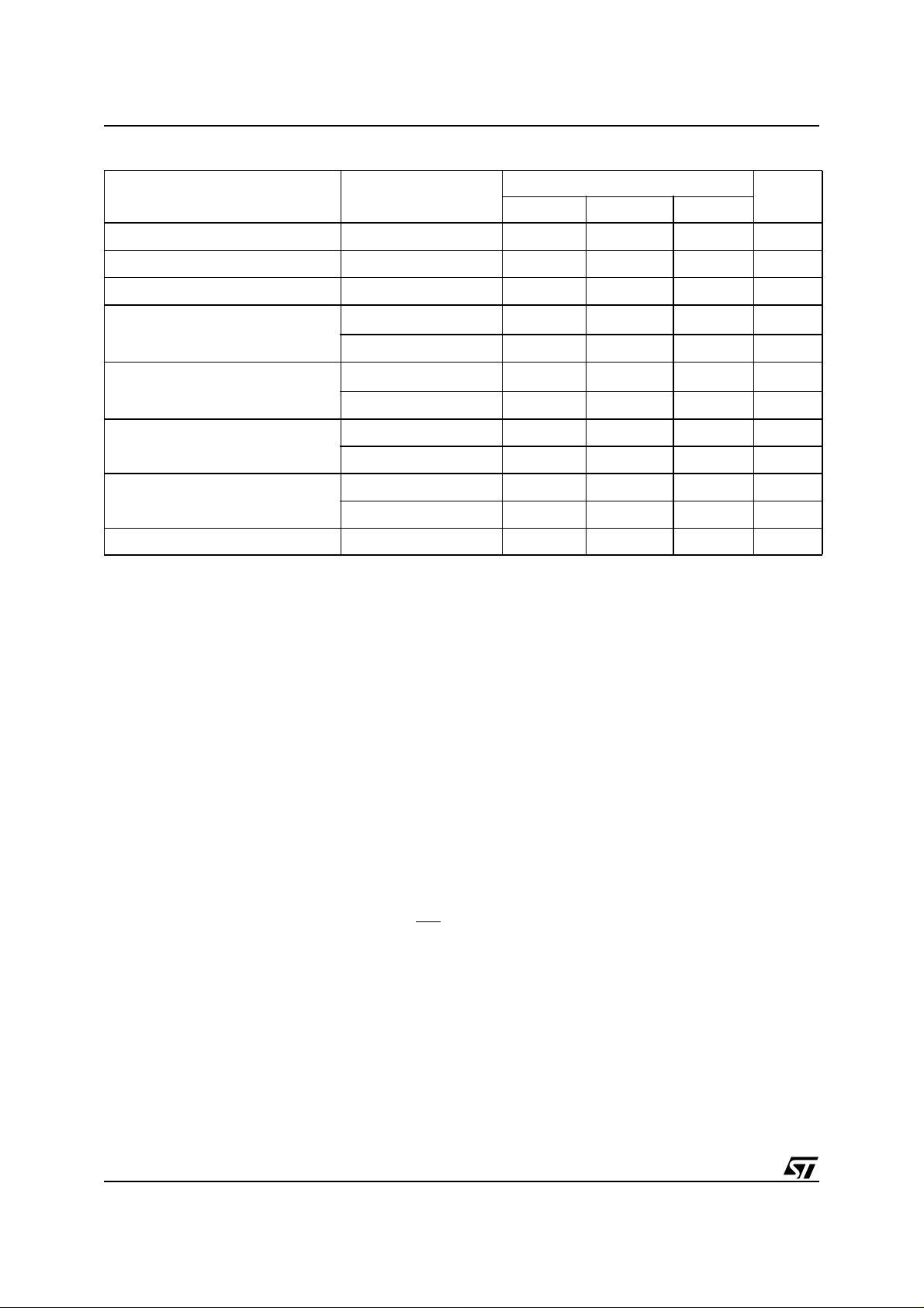
FEATURES SUMMARY
■ SUPPLY VOLTAGE
–V
–V
–V
■ ACCESS TIME
= 2.7V to 3.6V Core Power Supply
DD
= 1.65V to 3.3V for Input/Output
DDQ
= 12V for fast Program (optional)
PP
– 3.0V to 3.6V: 80ns
– 2.7V to 3.6V: 90ns
■ PROGRAMMING TIME:
– 10µs typical
– Double W ord Programming Option
– Quadruple Word Program ming Option
■ COMMON FLASH INTERFACE
■ MEMORY BLOCKS
– Parameter Blocks (Top or Bottom location)
– M ain Blocks
■ BLOCK LOCKING
– All blocks locked at Power Up
– Any combination of blocks ca n be locked
for Block Lock-Down
–WP
■ SECURITY
– 128 bit user Programmable OTP cells
– 64 bit unique device identifier
– One Parameter B lock Permanent ly Lockable
■ AUTOMAT IC STAND-BY MODE
■ PROGRAM and ERASE SUSPEND
■ 100,000 PROGRAM/ERASE CYCLES per
BLOCK
■ ELECTRONIC SIGNATURE
– Manufacturer Code: 20h
– Top Dev ice Code, M28W640CT: 8848h
– Bottom Device Code, M28W640CB: 8849h
M28W640CT
M28W640CB
64 Mbit (4Mb x16, Boot Block)
3V Supply Flash Memory
PRELIMINARY DATA
Figure 1 . Packages
FBGA
TFBGA48 (ZB)
8 x 6 ball array
TSOP48 (N)
12 x 20mm
November 2001
This is preliminary information on anew product nowin development or undergoing evaluation. Details are subject to change without notice.
1/54

M28W640CT, M28W640CB
TABLE OF CONTENTS
SUMMARYDESCRIPTION...........................................................5
Figure2.LogicDiagram ..........................................................5
Table 1. Signal Names . . . ........................................................5
Figure 3. TSOP Connec tions.......................................................6
Figure 4. TFBGA Connect ions (Top view through package). ..............................7
Figure5.BlockAddresses.........................................................8
Figure6.SecurityBlockMemoryMap................................................8
SIGNALDESCRIPTIONS............................................................9
AddressInputs(A0-A21)..........................................................9
Data I nput /O utpu t (DQ0-DQ15). . . ..................................................9
ChipEnable(E). ................................................................9
Output Enable (G). ..............................................................9
Write E nable (W). . ..............................................................9
WriteProtect(WP)...............................................................9
Reset(RP).....................................................................9
Supply V olt age (2.7V to 3.6V) ..................................................9
V
DD
V
Supply Vo lta ge (1.65V to VDD).................................................9
DDQ
ProgramSupplyVoltage ......................................................9
V
PP
V
Ground. ...................................................................9
SS
BUSOPERATIONS................................................................10
Read.........................................................................10
Write.........................................................................10
OutputDisable.................................................................10
Standby. . ....................................................................10
Automatic Standby. .............................................................10
Reset........................................................................10
Read Electronic Signature C ommand ...............................................11
Table2.BusOperations.........................................................10
COMMANDINTERFACE ...........................................................11
ReadMemoryArrayCommand....................................................11
ReadStatusRegisterCommand...................................................11
Read Electronic Signature C ommand ...............................................11
ReadCFIQueryCommand.......................................................11
BlockEraseCommand..........................................................11
ProgramCommand.............................................................11
Double Word Program Comm and . .................................................12
ClearStatusRegisterCommand...................................................12
Program/Erase Suspend Command ................................................12
Program/EraseResumeCommand ................................................12
ProtectionRegisterProgramCommand.............................................13
BlockLock-DownCommand......................................................13
2/54

M28W640CT, M28W640CB
Table3.Commands............................................................14
Table4.ReadElectronicSignature.................................................14
Table 5. Read Block Lock Signature ................................................15
Table6.ReadProtectionRegisterandLockRegister ..................................15
Table7.Program,EraseTimesandProgram/EraseEnduranceCycles ....................16
BLOCKLOCKING.................................................................16
LockedState..................................................................16
UnlockedState ................................................................16
Lock-DownState...............................................................17
Reading a Block’s Lock Status . . . .................................................16
LockingOperationsDuringEraseSuspend ..........................................17
Table8.BlockLockStatus .......................................................17
Table9.ProtectionStatus........................................................18
STATUSREGISTER...............................................................19
Program/EraseControllerStatus(Bit7).............................................19
Erase Suspend Status (Bit 6) .....................................................19
EraseStatus(Bit5).............................................................19
ProgramStatus(Bit4)...........................................................19
Status(Bit3)...............................................................19
V
PP
ProgramSuspendStatus(Bit2)...................................................19
BlockProtectionStatus(Bit1).....................................................20
Reserved(Bit0)................................................................20
Table10.StatusRegisterBits.....................................................20
MAXIMUMRATING................................................................21
Table11.AbsoluteMaximumRatings...............................................21
DCandACPARAMETERS .........................................................22
Table 12. Operating and AC Measurement C onditions..................................22
Figure7.ACMeasurementI/OWaveform ...........................................22
Figure 8. AC Measurement Load Circuit. . . ..........................................22
Table 13. Capacitance...........................................................22
Table14.DCCharacteristics......................................................23
Figure9.ReadACWaveforms....................................................24
Table15.ReadACCharacteristics.................................................24
Figure 10. Write AC Wavef orms, Write Enable Controlled . . .............................25
Table 16. Write AC Characteristics, Write Enable Controlled .............................26
Figure11.WriteACWaveforms,ChipEnableControlled................................27
Table17.WriteACCharacteristics,ChipEnableControlled .............................28
Figure12.Power-UpandResetACWaveforms.......................................29
Table18.Power-UpandResetACCharacteristics ....................................29
PACKAGE MECHANICAL . . . .......................................................30
3/54

M28W640CT, M28W640CB
Figure13.TSOP48-48leadPlasticThinSmallOutline,12x20mm,PackageOutline ........30
Table 19. TSOP48 - 48 lead Plastic Thin Small Outline, 12 x 20mm, Package M echanical Data . 30
Figure14.TFBGA48-8x6ballarray,0.75mmpitch,BottomViewPackageOutline .........31
Table20.TFBGA48-8x6ballarray,0.75mmpitch,PackageMechanicalData.............31
Figure 15. TFBGA48 Daisy Chain - Package Connections (Top view through package) ........32
Figure 16. TFBGA48 Daisy Chain - P C B Connections propo sal (Top view through package)....32
PARTNUMBERING ...............................................................33
Table21.OrderingInformationScheme.............................................33
Table22.DaisyChainOrderingScheme............................................33
REVISIONHISTORY...............................................................34
Table23.DocumentRevisionHistory...............................................34
APPENDIX A. BLOCK ADDRESS TABLES . . ..........................................35
Table 24. Top Boot Block Addresses, M28W640CT....................................35
Table25.BottomBootBlockAddresses,M28W640CB.................................37
APPENDIXB.COMMONFLASHINTERFACE(CFI) .....................................39
Table26.QueryStructureOverview................................................39
Table 27. CFI Query Identification String . . ..........................................39
Table28.CFIQuerySystemInterfaceInformation.....................................40
Table29.DeviceGeometryDefinition...............................................41
Table 30. Primary Algorithm-Specific Extended Query Table .............................42
Table31.SecurityCodeArea.....................................................43
APPENDIX C. FLOWCHARTS AND P SEUDO CODES....................................44
Figure 17. Program Flowchart and Pseudo Code . . ....................................44
Figure 18. Double Word P rogram Flowchart and Pseudo Code ...........................45
Figure 19. Quadruple Word Program Flowchart and Pseudo Code . .......................46
Figure 20. Program Suspend & Resume Flowchart and Pseudo Code .....................47
Figure 21. Erase Flowchart and Pseudo Code ........................................48
Figure 22. Erase Suspend & Resume Fl owchart and Pseudo Code. .......................49
Figure 23. Locking Operations Flowchart and Pseudo Code .............................50
APPENDIXD.COMMANDINTERFACEANDPROGRAM/ERASECONTROLLERSTATE.......52
Table32.WriteStateMachineCurrent/Next,sheet1of2................................52
Table33.WriteStateMachineCurrent/Next,sheet2of2................................53
4/54
SUMMARY DESCRIPTION
The M28W640C is a 64 Mbit (4 Mbit x 16)non-volatileFlashmemorythatcanbeerasedelectrically
at the block leveland programmed in-system on a
Word-by-Word basis. These operations can be
performed using a single low voltage (2.7 to 3.6V)
supply. V
1.65V. An optional 12V V
allows to drive the I/O pin down to
DDQ
power supply is pro-
PP
vided to speed up customer programming.
The device features an asymmetrical blocked ar-
chitecture. The M28W640C has an array of 135
blocks: 8 Parameter Blocks of 4 KWord and 127
Main Blocks of 32 KWord. M28W640CT has the
Parameter Blocks at the top of the memory address space while the M28W640CB locates the
Parameter Blocks starting from the bottom. The
memory maps are shown in Figu re 5, Block Addresses.
The M28W640C features an instant, individual
block locking scheme that allows any block to be
locked or unlocked with no latency, enabling instant code and data protection. All blocks have
three levels of protection. They can be locked and
locked-down individually preventing any accidental programming or erasure. There is an additional
hardware protection against program and erase.
When V
PP
≤ V
all blocksare protected against
PPLK
program or eras e. All blocks are locked at Power
Up.
Each block can be erased separately. Erase can
be suspended in order to perform either read or
program in any other block and then resum ed.
Program can be sus pended to read d ata in any
other block and then resumed. Each block can be
programmed and erased over 100,000 cycles.
The device includes a 192 b it Protection Register
and a Security Block to increase the protection of
a system design. The Protection Register is divided into a 64 bit segment and a 128 bit segment.
The 64 bit segment contains a unique device number written by ST, while the second one is onetime-programmable by the user. The user programmable segment can be permanently prot ec ted. The Security Block, parameter block 0, can be
permanently protected by the user. Figure 6,
shows the Security Block M emory Map.
Program and Erase commands are written to the
Command Interface of the memory. An on-chip
Program/Erase Control ler takes care of the timings necessary for program and erase operations.
The end of a program or erase operation can be
detected and any error conditions identified. The
command set required to control the memory is
consistent with JEDEC standards.
M28W640CT, M28W640CB
ThememoryisofferedinTSOP48(12X20mm)
and TFBG A48 (0.75mm pitch) packages and is
suppliedwithallthebitserased(setto’1’).
Figure 2. Logic Diagram
V
V
DD
DDQVPP
22
A0-A21
W
E
G
RP
WP
M28W640CT
M28W640CB
V
SS
Table 1. Signal Names
A0-A21 Address Inputs
DQ0-DQ15 Data Input/Output
E
G
W
RP
WP
V
DD
V
DDQ
V
PP
V
SS
NC Not Connected Internally
Chip Enable
Output Enable
Write Enable
Reset
Write Protect
Core Power Supply
Power Supply for
Input/Output
Optional Supply Voltage for
Fast Program & Erase
Ground
16
DQ0-DQ15
AI04378
5/54
M28W640CT, M28W640CB
Figure 3. TSOP Connections
A15
A14
A13
A12
A11
1
48
A16
V
DDQ
V
SS
DQ15
DQ7
A10 DQ14
37
36
DQ6
DQ13
DQ5
DQ12
DQ4
V
DD
DQ11
DQ3
DQ10
DQ2
DQ9
DQ1
DQ8
DQ0
G
V
SS
E
A0
A21
A20
RP
V
PP
WP
A19
A18
A17
A9
A8
W
A7
A6
A5
A4
A3
A2
A1
12
M28W640CT
M28W640CB
13
24 25
AI04379
6/54
Figure 4. TFBGA Connections (Top view through package)
M28W640CT, M28W640CB
87654321
A
B
C
D
E
F
A13
DDQ
SS
DQ7V
A8A11
DQ13
PP
RP A18
A21
DQ11
DQ12
DQ4
WP A19
A20
DQ2
DD
A7V
DQ0DQ9DQ3DQ6DQ15V
DQ1DQ10V
A4
A2A5A17WA10A14
A1A3A6A9A12A15
A0EDQ8DQ5DQ14A16
V
SS
G
AI04380
7/54
M28W640CT, M28W640CB
Figure 5. Block Addresse s
M28W640CT
Top Boot Block Addresses
3FFFFF
3FF000
3F8FFF
3F8000
3F7FFF
3F0000
00FFFF
008000
007FFF
000000
Note: Also see Appendix A, Tables 24 and 25 for a full listing of the Block Addresses.
4 KWords
Total of 8
4 KWord Blocks
4 KWords
32 KWords
Total of 127
32 KWord Blocks
32 KWords
32 KWords
Bottom Boot Block Addresses
3FFFFF
3F8000
3F7FFF
3F0000
00FFFF
008000
007FFF
007000
000FFF
000000
M28W640CB
32 KWords
32 KWords
Total of 127
32 KWord Blocks
32 KWords
4 KWords
Total of 8
4 KWord Blocks
4 KWords
AI04386
Figure 6. Security Block Memory Map
Parameter Block # 0
8Ch
85h
84h
81h
80h
User Programmable OTP
Unique device number
Protection Register Lock 2 1 0
AI04397
8/54

SIGNAL DESCRIPTIONS
See Fig ure 2 Logic Diagram and Table 1,Signal
Names, for a brief overview of the signalsconnected to this device.
Address Inputs (A0-A21). The Address Inputs
select the cells in the memory array to access during Bus Read operations. During Bus Write operations they control the commands sent to the
Command Int erface of the int ernal state machine.
Data Input/Output (DQ0-DQ15). The Data I/O
outputs the data stored at t he s elected address
during a Bus Read operation or inputs a command
orthedatatobeprogrammedduringaWriteBus
operation.
Chip Enable (E
). The Chip Enable input acti-
vates the memory control logic, input buffers, decoders and sense amplifiers. When Chip Enable is
and Reset is at VIHthe device is in active
at V
IL
mode. When Chip Enable is at V
the m emory is
IH
deselected, the outputs are hi gh impedance and
the power consumption is reduced to the stand-by
level.
Output Enable (G
). The Output Ena ble controls
data outputs during the Bus Read operation of the
memory.
WriteEnable(W
). Th e Write E nable controls the
Bus Write operation of the memory’s Command
Interface. The dataand address inputs are latched
ontherisingedgeofChipEnable,E,orWriteEnable, W
Write Protect (WP
, whichever occurs first.
). Write Protect is an input
that gives an additional hardware protection for
each block. When Write Protect is at V
, the Lock-
IL
Down is enabled and the protection status of the
block cannot be c hanged. When Write Protect is at
V
, the Lock-Down is disabled and the block can
IH
be lock ed or unlocked. (refer to Table 6, ReadProtection Register and Protection Register Lock).
Reset (RP
wareresetofthememory.WhenResetisatV
). The Reset input provides a hard-
IL
the memory is in reset mode: the outputs are high
impedance and the current consumption is minimized. After Reset all blocks are in the Locked
state. WhenRe set is at V
, thedevice is in normal
IH
M28W640CT, M28W640CB
operation. Exiting reset mode the device enters
read array mode, but a negative trans ition of Chip
Enable or a change of the address is required to
ensure valid data outputs.
V
Supply Voltage (2.7V to 3.6V). VDDpro-
DD
vides the power supply t o the internal core of the
memory dev ice. It is the main power supply for all
operations (Read, Program and Erase).
Supply Voltage (1.65V to VDD). V
V
DDQ
provides the power supply to the I/O pins and enables all Outputs to be powered independently
from V
DD.VDDQ
separate supply.
Program Supply Voltage. VPPis both a
V
PP
control input and a power supply pin. The two
functions are selected by the voltage range applied to the pin. The Supply Voltage V
Program Supply Voltage V
anyorder.
is kept in a low voltage range (0V to 3.6V)
If V
PP
V
is seen as a control input. In this case a volt-
PP
age lower than V
against program or erase, while V
ables these func tions (see Table 14, DC Characteristics for the relevant values). V
sampled at the beginning of a program or eras e; a
change in its value after the operation has started
does not have any effect on Program or Erase,
however for Double or Quadruple Word Program
the results are uncertain.
If V
is in the range 11.4V to 12.6V it acts as a
PP
power supply pi n. In this condition V
stable until the Program/Erase algorithm is completed (see Table 16 and 17).
Ground. VSSis the reference for all voltage
V
SS
measurements.
Note: Each device i n a system should have
V
DD,VDDQ
pacitor close to the pin. See Figure 8 , AC Mea-
,
surement Load Circuit. Th e P CB trace widths
should be sufficient to carry the required V
program and erase currents.
canbetiedtoVDDor can use a
canbeappliedin
PP
gives an absolute protection
PPLK
PP
and VPPdecoupled with a 0.1µF ca-
DD
>V
PP
PP
DDQ
and the
en-
PP1
is only
must be
PP
9/54
M28W640CT, M28W640CB
BUS OPERATIONS
There are s ix standard bus operations that control
the device. These are Bus Read, Bus Write, Output Disable, Standby, Automatic Standby and Reset. See Table 2, B us Operations, for a summary.
Typically glitch es of less t han 5ns on Chip Enable
or Write Enable areignored by the memory and do
not affect bus operations.
Read. Read B us operations are used to ou tput
the contents of the Memory Array, the Electronic
Signature, the Status R egister and the Comm on
Flash Interface. Both Chip E nable and Output EnablemustbeatV
eration. The Chip Enable input should be used to
enable the device. Output Enable should be used
to gate data onto the output. The data r ead depends on the previous command written to the
memory (see Command Interface s ec tion). See
Figure 9, Read Mode AC Waveforms , a nd Table
15, Read AC Charac t erist ics, for details of when
the output becomes valid.
Read mode is the default stat e of t he device when
exiting Reset or after power-up.
Write. B us Write operations write Commands to
the memory or latch Input Data to be programmed.
A write operation is initiated when Chip Enable
and Write Enable are at V
. Commands, Input Data and Addresses are
V
IH
latched on the rising edge of Write Enable or Chip
Enable, whichever occurs first.
in order to perform a read op-
IL
with Output Enable at
IL
See Figures 10 and 1 1, WriteAC Waveforms, and
Tables 16 and 17, Write AC Characteristics, for
details of the timing requirements.
Output Disable. The data outputs are high impedance when the Output Enable is at V
.
IH
Standby. S tandby disables most of the internal
circuitryallowing a substantial reduction of t he current consumption. The memory is in stand-by
when Chip Enable is at V
andthedeviceisin
IH
read mode. The power consumption is reduced to
the stand-by level and the outputs are set to high
impedance, independently from theOutput E nable
or Write Enable inputs. If Chip Enable switches to
V
during a program or erase operation, the de-
IH
vice enters Standby mode when finished.
Automatic Standby. Automatic Standby pro-
vides a low power cons umption state during Read
mode. Following a read operation, the device enters Automatic Standby after 150ns of bus inactivity even if Chip Enable is Low, V
current is reduced to I
. The data I nputs/Out-
DD1
, and the supply
IL
puts will still output data if a bus Read operation is
in progress.
Reset. During Reset mode when Output Ena ble
is Low, V
, the memory is deselec ted andthe ou t-
IL
puts are high impedance. The memory is in Reset
mode when Reset is at V
. The power consump-
IL
tion is reduc ed to the Standby level, independent ly
from the Chip Enable, Output Enable or Write E nable inputs. If Reset is pulled to V
during a Pro-
SS
gram or Erase, this operation is aborted and the
memory conten t is no longer valid.
Table 2. Bus Operations
Operation E G W RP WP
Bus Read
Bus Write
Output Disable
Standby
Reset X X X
Note: X = VILor VIH,V
10/54
V
V
V
V
=12V±5%.
PPH
IL
IL
IL
IH
V
IL
V
IH
V
IH
XX
V
IH
V
IL
V
IH
V
IH
V
IH
V
IH
V
IH
V
IL
V
PP
X Don't Care Data Output
V
X
X Don't Care Hi-Z
X Don't Care Hi-Z
X Don't Care Hi-Z
DD
or V
PPH
DQ0-DQ15
Data Input

COMMAND INTERFACE
All B us Write operations to the memory are interpreted by the Command Interface. Commands
consist of one or more sequential Bus Write operations. An internal Program/Erase Controller handles all timings and verifies the correct execution
of the Program and Erase commands. The Pr ogram/Erase Controller provides a Status Register
whose output may be read at any time during, to
monitor the progress of the operation, or the Program/Erase states. See Appendix 22, Table 32,
Write State Machine Current/Next, for a summary
of the Command Interface.
The Command Interface is res et to Read mode
when power is f irst applied, when exiting from R eset or whenever V
is lower than V
DD
LKO
.Command sequences must be followed exactly. A ny
invalid c ombination of c ommands will reset the device to Read mode. Refer to Table 3, Commands,
in conjunction with the text descriptions below.
Read Memory Array Command
TheReadcommandreturnsthememorytoits
Read mode. O ne Bus Write cycle is requ ired toissue the Read Mem ory Array command and return
the memory to Read mode. S ubs equent read operations will read the addressed location and output the data. When a device Reset occ urs, the
memory defaults to Read m ode.
Read Status Register Command
The Status Regist er indicates when a program or
erase operation is complete and the success or
failure of the operation itself. Issue a Read Status
Register command to read the Stat us Register’s
contents. Subsequent Bus Read operations read
the Status Register at any address, u nti l another
command isissued. See Table 10, Status Register
Bits, for details on the definitions of the bits.
The Re ad Status Register command may be issued at any time, even during a Program/Erase
operation. Any Read atte mpt during a Program/
Erase operation will automatically output the content of the Status Register.
Read Electronic Signature Command
The Read Electronic Sig natu re command reads
the Manufacturer and Device Codes and the B lock
Locking S tatus, or the Protection Regis ter.
The Read Electronic Signature command consists
of one write cycle, a subsequent read will output
the Manufacturer Code, the D ev ice Code, the
Block Lock and Lock-Down Status, o r the Protection and Lock R egister. S ee Tables 4, 5 and 6 for
the valid address.
Read CFI Query Command
The Read Query Command is used t o read dat a
from the Commo n Flash Interface (CFI) Memory
Area, allowing programming equi pment or appli-
M28W640CT, M28W640CB
cations to automatically match their interface to
the characteristics of t he device. One Bus Write
cycle is required to issue the Read Query Com mand. Once the command is issued subsequent
Bus Read operations read from the Common
Flash Interface Memory Area. See Appendix B,
Common Flas h Interface, Tables 26, 27, 28, 29,
30 and 31 for det ails on the information c ontained
in the Common Flash Interface memory area.
Block Erase Command
TheBlockErasecommandcanbeusedtoerase
a block. It sets all the bits within the selected block
to ’1’. All previous data in the block is lost. If the
block is protected then the Erase operation w ill
abort, the data in the block will not be changed and
the Status Register will output the error.
Two Bus Write cycles are required to issue the
command.
■ Th e first bus cycle sets up the Erase com mand.
■ Th e second latches the block addres s in the
internal state machine and starts the P ro gram/
Erase Co ntroller.
If the second bus cycle is not Write Erase Co nfirm
(D0h), S ta tus Register bits b4 and b5 are s et and
the command aborts.
Erase aborts if Reset turns to V
cannot beguaranteed when t he Erase operation is
aborted, the block must be erased agai n.
During Erase operations the mem ory will accept
the Read S tatus Register command and the Program/Erase Suspend command, all other commands will be ignored. Typical Erase times are
given in Table 7, Program , Erase Times and Program/Erase End uranc e Cycles.
See Appendix C, Figure 21, Erase Flowchart and
Pseudo Code, for a suggested flowchart for using
the Erase command.
Program Command
The memory array can be programmed word-byword. Two bus write cycles are required to issue
the Program Command.
■ Th e first bus cycle s ets up the Program
command.
■ Th e second latchesthe Address and the Datato
be written and starts the Program/Erase
Controller.
During Program operations the memory will accept the Read Status Register command and the
Program/Erase S uspend com mand. Typical Program times are given in Table 7, Program, Erase
Times and Program/Erase Endurance Cycles.
Programming aborts if Reset goes to V
integrity cannot be guaranteed when the program
operation is aborted, the block containing the
. As data integrity
IL
. A s data
IL
11/54

M28W640CT, M28W640CB
memory location must be erased and reprogrammed.
See Appendix C, Figure 17 , Program Flowchart
and Pseudo Code, for the flowchart for using the
Program command.
Double Word Program Command
Thisfeat ure is offered to improve the programming
throughput, writing a page of two adjacent words
in parallel.The two words must di ffer on ly for t he
address A0. P r ogramming should not be attempted when V
executed if V
isnot at V
PP
PP
is below V
PPH
. The command can be
but the result is not
PPH
guaranteed.
Three bus write cycles are necessary to issue the
Double Word Program command.
■ Th e first bus cycle sets up t he Double Word
Program Command.
■ The second bus cycle l atches the Address and
theDataofthefirstwordtobewritten.
■ The third bus cycle latches the Address and the
Data ofthe second word to be written and starts
the Program/Erase Controller.
Read operations output the Status Register content after the programm ing has started. Programming aborts if Reset goes to V
. As data integrity
IL
cannot be guaranteed when the program operation is aborted, the block containing the memory
location mu st be erased and repro gramm ed.
See Appendix C, Figure 18, Double Word Program Flowchart and Pseudo Code, for the f lowchart for using the Double Word Program
command.
Quadruple Word Program Command
Thisfeat ure is offered to improve the programming
throughput, writing a page of four adjacent words
in parallel.The four words must differ only for the
addresses A0 andA1. Program ming s hould not be
attempted when V
PP
can be executed if V
isnotatV
is below V
PP
.The command
PPH
but theresult
PPH
is not guaranteed.
Five bus write c ycles are necessary to issue the
Quadruple Word Program command.
■ Th e first bus cycle sets up t he Double Word
Program Command.
■ The second bus cycle l atches the Address and
theDataofthefirstwordtobewritten.
■ The third bus cycle latches the Address and the
Data of the second word to be writte n.
■ The fourth bus cycle latches the Address and
theDataofthethirdwordtobewritten.
■ The fifth bus cycle latches the Address and the
Data of the fourth wo rd tob e written and starts
the Program/Erase Controller.
Read operations output the Status Re gister content after the programm ing has started. Programming aborts if Reset goes to V
. As data integrity
IL
cannot be guaranteed when the program operation is aborted, the block containing the memory
location mu st be erased and repro gramm ed.
See Appendix C, Figure 19, Quadruple Word Program Flowchart and Pseudo Code, for the f lowchart for usin g the Quadruple Word Program
command.
Clear Status R egister Command
The Clear Status Register command can be us ed
to reset bits 1, 3, 4 and 5 in the Status Register t o
‘0’. One bus write cycle is required t o issue the
Clear Status Register command.
The bits in the StatusRegiste r donot automatically return to ‘0’ when a n ew Program or E r as e command is issued. The error bits in the Status
Register should be cleared before attempting a
new Prog ram or Erase command.
Program/Erase Suspend Command
The Program/Erase Sus pend command is used to
pause a Pr ogram or Erase operation. One bus
write cycle is required to iss ue the Program/Erase
command and pause the Program/Erase controller.
During Program/Erase Suspend the Co mmand Interface will accept the Program/E ras e Resu me,
Read A rray , Read Status Register, Read E lectronic Signature and Read CFI Query commands. Additionally, if the suspend operation was Erase then
the Program, Double Word Program, Quadruple
Word Program, Block Lock, B lock Lock-Down or
Protection Program commands will also be accepted. Th e block being erased may be pro tected
by issuing the Block Protect, Block Lock or Protection Program commands. When the Program/
Erase Resume command is issued the operation
will complete. Only the blocks not being erased
may be read or prog ramm ed correctly.
During a Program/Erase Su sp end, the device can
be placed in a pseudo-standby mode by taking
Chip Enable to V
Reset t urns to V
. Program/Erase i s aborted if
IH
.
IL
See Appendix C, Figure 20, Program Suspend &
Resume Flowchart and Pseudo Code, and Figure
22, Erase Sus pend & Resume Flowchart and
Pseudo Codefor flowcharts for using the Program/
Erase Suspend command.
Program/Erase Resume Command
The Program/Erase Resume command can be
used to restart the Program/Erase Controller after
a Program/Erase Suspend operation has paused
it. One Bus W rite cycle is required to issue the
command. Once the command is issued subse-
12/54

M28W640CT, M28W640CB
quent Bus Read operations read t he Status Register.
See Appendix C, Figure 20, Program Suspend &
Resume Flowchart and Pseudo Code, and Figure
22, Erase Sus pend & Resume Flowchart and
Pseudo Codefor flowcharts for using the Program/
Erase Resume command.
Protection Register Program Command
The Protection R egister Program command is
used to Program the 128 bit user One-Time-Programmable (OTP) segment of the Protection Register. The segment is programmed 16 bits at a
time. When shipped all bits in the segment are set
to ‘1’. The user can onlyprogram the bits to ‘0’.
Two write cycles are required to issue the Protection Register Program command.
■ Th e first bus cycle s ets up the Protection
Register Program command.
■ Th e second latchesthe Address and the Datato
be written to the Protection Register and starts
the Program/Erase Controller.
Read operations output the Status Register content after the programming has started.
The segment can be prot ec ted by programming bit
1 of t he Protection Lock Register. Bit 1 of the Protection Lock Register protects bit 2 of the Protection Lock Register. Programming bit 2 of the
Protection Lock Register will result in a permanent
protection of the Security Block (see Figure 6, Security Block Memory Map). Attempting to program
a previously protected Protection Register will result in a Status Register error. The protection of
the Protection Register and/or the Security Block
is not reversible.
The Protection Register Program ca nnot be suspended.
Block Lock Command
The Block Lock command is used to lock a block
and prevent Program or Erase operations from
changing the data in it. All blocks are lock ed at
power-up or reset.
Two Bus Write cycles are required to issue the
Block Lock command.
■ Th e first bus cycle s ets up the Block Loc k
command.
■ The second Bus W rite cycle latches the block
address.
The lock status can be monitored for each block
using the Read Electronic Signature command.
Table. 9 shows the protection status after issuing
a Block Lock command.
The Block Lock bits are volatile, onc e set they remain set until a hardware reset or power-down/
power-up. They are cleared by a Blo cks Unlock
command. Refer to the section, Block Locking, for
a detailed explanation.
Block Unlock Command
The Blocks Unlock command is used to unlock a
block, allowing the block to be programmed or
erased. Two Bus Write cycles are required to issue the Blocks Unlock command.
■ Th e first bus cycle s ets up the Block Unlock
command.
■ The second Bus W rite cycle latches the block
address.
The lock status can be monitored for each block
using the Read Electronic Signature command.
Table. 9 shows the protection status after issuing
a Block Unlock command. Refer to t he section,
Block Locking, for a detailed explanati on.
Block Lock-Down Command
A locked block cannot be Programmed or Erased,
or have its protection status changed when WP
low, V
.WhenWPis high, V
IL
the Lock-Down
IH,
function is disabled and the lock ed blocks can be
individually unlocked by the Block Unlock command.
Two Bus Write cycles are required to issue the
Block Lock-Down command.
■ Th e first bus cycle s ets up the Block Loc k
command.
■ The second Bus W rite cycle latches the block
address.
The lock status can be monitored for each block
using the Read Electronic Signature command.
Locked-Down blocks revert to the locked (and not
locked-down) state when the device is reset on
power-down. Table. 9 shows the protection status
after issuing a Block Lock-Down command. Refer
to the section, Block Lockin g, for a detailed explanation.
is
13/54
M28W640CT, M28W640CB
Table 3. Commands
Bus Write Operations
Commands
Read Memory
Array
Read Status
Register
Read Electronic
Signature
Read CFI Query 1+ Write X 98h Read QA QD
Erase 2 Write X 20h Write BA D0h
Program 2 Write X
Double Word
Program
QuadrupleWord
Program
Clear Status
Register
Program/Erase
Suspend
Program/Erase
Resume
Block Lock 2 Write X 60h Write
Block Unlock 2 Write X 60h Write
Block Lock-Down 2 Write X 60h Write
Protection Register
Program
Note: 1. X = Don't Care, RA=Read Address, RD=Read Data, SRD=Status Register Data, ID=Identifier (Manufacture and Device Code),
(3)
(4)
QA=Query Address, QD=Query Data, BA=Block Address, PA=Program Address, PD=Program Data, PRA=Protection Register Address, PRD=Protection Register Data.
2. The signature addresses are listed in Tables 4, 5 and 6.
3. Program Addresses 1 and 2 must be consecutive Addresses differing only for A0.
4. Program Addresses 1,2,3 and 4 must be consecutive Addresses differing only for A0 and A1.
1st Cycle 2nd Cycle 3rd Cycle 4th Cycle 5th Cycle
Cycles
Op. Add Data Op. Add Data Op. Add Data Op. Add Data Op. Add Data
1+ Write X FFh
1+ Write X 70h Read X SRD
1+ Write X 90h Read
40h
or
10h
3 Write X 30h Write PA1 PD1 Write PA2 PD2
5 Write X 55h Write PA1 PD1 Write PA2 PD2 Write PA3 PD3 Write PA4 PD4
1Write X 50h
1Write X B0h
1Write X D0h
RA RD
Read
(2)
IDh
SA
Write PA PD
01h
BA
BA D0h
2Fh
BA
2 Write X C0h Write
PRA PRD
Table 4. Read Electronic Signature
Code Device E G W A0 A1 A2-A7 A8-A21 DQ0-DQ7 DQ8-DQ15
Manufacture.
Code
M28W640CT
Device Code
M28W640CB
Note: RP =VIH.
14/54
V
V
V
V
IL
IL
IH
V
V
IL
V
IL
V
IL
IH
V
V
IL
IH
IL
V
IHVIL
V
IHVIL
V
0 Don't Care 20h 00h
IL
0 Don't Care 48h 88h
0 Don't Care 49h 88h
M28W640CT, M28W640CB
Table 5. Read Block Lock Signature
Block Status E G W A0 A1 A2-A7 A8-A11 A12-A21 DQ0 DQ1 DQ2-DQ15
Locked Block
Unlocked Block
Locked-Down
Block
Note: 1. A Locked-Down Block can be locked "DQ0 = 1" or unlocked "DQ0 = 0"; see Block Locking section.
V
ILVILVIHVILVIH
VILVILVIHVILV
V
ILVILVIHVILVIH
0 Don't Care Block Address 1 0 00h
0 Don't Care Block Address 0 0 00h
IH
0 Don't Care Block Address
Table 6. Read Protection Register and Lock Register
Word E
Lock
Unique ID 0
Unique ID 1
Unique ID 2
Unique ID 3
OTP 0
OTP 1
OTP 2
OTP 3
OTP 4
OTP 5
OTP 6
OTP 7
G W A0-A7 A8-A21 DQ0 DQ1 DQ2 DQ3-DQ7 DQ8-DQ15
V
ILVILVIH
V
ILVILVIH
VILVILV
V
ILVILVIH
V
ILVILVIH
V
ILVILVIH
V
ILVILVIH
V
ILVILVIH
V
ILVILVIH
V
ILVILVIH
VILVILV
V
ILVILVIH
V
ILVILVIH
80h Don'tCare 0
OTP Prot.
data
81h Don't Care ID data ID data ID data ID data ID data
82h Don't Care ID data ID data ID data ID data ID data
IH
83h Don't Care ID data ID data ID data ID data ID data
84h Don't Care ID data ID data ID data ID data ID data
85h Don't Care OTP data OTP data OTP data OTP data OTP data
86h Don't Care OTP data OTP data OTP data OTP data OTP data
87h Don't Care OTP data OTP data OTP data OTP data OTP data
88h Don't Care OTP data OTP data OTP data OTP data OTP data
89h Don't Care OTP data OTP data OTP data OTP data OTP data
8Ah Don't Care OTP data OTP data OTP data OTP data OTP data
IH
8Bh Don't Care OTP data OTP data OTP data OTP data OTP data
8Ch Don't Care OTP data OTP data OTP data OTP data OTP data
Security
prot. data
(1)
X
00h 00h
1 00h
15/54
M28W640CT, M28W640CB
Table 7. Program, Erase Times and Program/Erase Endurance Cycles
Parameter Test Conditions
Word Program
Double Word Program
Quadruple Word Program
Main Block Program
Parameter Block Program
Main Block Erase
Parameter Block Erase
Program/Erase Cycles (per Block) 100,000 cycles
Note: 1. Typicaltime to programa Main or Parameter Blockusing the Double WordProgram andtheQuadrupleWord Program commands
respectively.
V
PP=VDD
V
= 12V ±5%
PP
= 12V ±5%
V
PP
= 12V ±5%
V
PP
V
PP=VDD
V
= 12V ±5%
PP
V
PP=VDD
= 12V ±5%
V
PP
V
PP=VDD
= 12V ±5%
V
PP
V
PP=VDD
Min Typ Max
M28W640C
10 200 µs
10 200 µs
10 200 µs
0.16/0.08
0.02/0.01
(1)
0.32 5 s
(1)
0.04 4 s
110s
110s
0.8 10 s
0.8 10 s
5s
4s
Unit
BLOCK LOCKING
The M28W640C features an instant, individual
block locking scheme that allows any block to be
lockedorunlockedwithnolatency.Thislocking
scheme has three levels of protection.
■ Lock/Unlock - this first level allows software-
only contro l of block locking.
■ Lock-Down - this second level requires
hardware interaction before locking can be
changed.
■ V
PP
≤ V
- the third level of fers a complete
PPLK
hardware prot ection against program anderase
on all blocks.
Theprotectionstatusofeachblockcanbesetto
Locked, Unlocked, and Lock-Down. Table 9, defines all of the possible protection states (WP
DQ1, DQ0), and Appendix C, F igure 23, shows a
flowchart for the locking operations.
ReadingaBlock’sLockStatus
The lock s ta tus of every block can be read in the
Read Electronic Signature mode of the device. To
enter this mode write 90h to the device. Subsequent reads at the address spe cified in Table 5,
will output the protection status of that block. The
lock status is represented by DQ0 and DQ1. DQ0
indicates the Block Lock/Unlock status and is set
by the Loc k command and cleared by the Unlock
command. It is also automatically set when enteringLo ck-Down . DQ1 indicates the Lock-Down status and is set by the Lock-Down c ommand. It
cannot be cleared by software, only by a hardware
reset or power-down.
The following sections explain theoperation ofthe
locking system.
Locked State
The defau lt status of all blocks on power-up or after a hardware reset is Locked (states (0,0,1) or
(1,0,1)). L oc ked block s are fully protec te d from
any program or erase. Any program or erase operations attempted on a locked block will return an
error in the Status Register. The Status of a
Locked block can be changed to Unlocked or
Lock-Down using the appropriate software com-
,
mands.An Unlocked block can be Locked by issuing the Lock command.
Unlocked State
Unlocked b lock s (states (0,0,0), (1,0,0) (1,1,0)),
can be programmed or erased. All unlocked
blocks return to the Locked state after a h ardware
reset or when the device is powered-down. The
status of an unlocked bloc k can be changed to
Locked or Locked-Down using the appropriate
software commands. A lo cked block can be unlocked by issuing the Unlock command.
16/54
M28W640CT, M28W640CB
Lock-Down State
Blocks that are Locked-Down (state (0,1,x))are
protected from program and erase operations (as
for Loc k ed blocks) but their protection status cannot be changed using software commands alone.
A Locked or Unlocked block can be Locked-Down
by issuing the Lock-Down command. LockedDown blocks revert to the Locked state when the
device is reset or powered-down.
The Lock-Down fu nction is dependent on the WP
input pin. When WP=0 (VIL), the blocks in the
Lock-Down state (0,1,x) are protected from program, erase and protection status changes. When
WP
=1 (VIH) the Lock-Down function is disabled
(1,1,1) and Locked-Down blocks can be individually unlocked to the (1,1,0) state by iss uing the
software comm and, where they can be erasedand
programmed. These blocks c an then be relocked
(1,1,1) and unlocked (1,1,0) as desired while WP
remains high. When WP is low , blocks that were
previously Locked-Down return to the Lock-Down
state (0,1,x) regardless of any changes made
while WP
was high. Device reset or power-down
resets all blocks , including those in Lock-Down, to
the Locked state.
Locking Operations During Erase Suspend
Changes to block lock status can be performed
during an erase suspend by using the standard
locking command sequences to unlock, lock or
lock-down a block. This is useful in the case when
another block needs to be updated while an erase
operation is in progress.
To change block locking d uring an erase operation, first write the Erase Suspend command, then
check the status registe r until it indicates that the
erase operation has been suspended. Next write
the desired Lock com mand sequence to a block
and the lock status will be changed. After completing any des ired lock, read, or program operations,
resume the erase operation with the Erase Resume com mand.
If a block is locked or locked-down during an erase
suspend of the same bl ock, the locking status bits
will be changed immediately, but when the erase
is resumed, the erase operat ion will complete.
Locking operations cannot be performed during a
program su sp end. Refer to Appendix D, Command Interface and Program/Erase Controller
State, for detailed information on which commands are valid during erase suspend.
Table 8. Block Lock Status
Item Address Data
Block Lock Configuration
Block is Unlocked DQ0=0
Block is Locked DQ0=1
Block is Locked-Down DQ1=1
LOCK
xx002
17/54
 Loading...