

SGS Thomson Microelectronics M28R400C Datasheet

1/50March 2003
M28R400CT
M28R400CB
4 Mbit (256Kb x16, Boot Block)
1.8V Supply Flash Memory
FEATURES SUMMARY
■ SUPPLY VOLTAGE
–V
DD
= 1.65V to 2.2V Core Power Supply
–V
DDQ
= 1.65V to 2.2V for Input/Output
–V
PP
= 12V for fast Program (optional)
■ ACCESS TIMES: 90ns, 120ns
■ PROGRAMMING TIME
– 10µs typic al
– Double Word Programming Option
■ COMMON FLASH INTERFACE
– 64 bit Security Code
■ MEMORY BLOCKS
– Parameter Blo cks (Top or Bottom location)
– Main Blocks
■ BLOCK LOCKING
– All blocks locked at Power Up
– Any combination of blocks can be locked
–WP
for Block Lock-Down
■ SECURITY
– 64 bit user Programmable OTP cells
– 64 bit unique device identifier
– One Parameter Block Permanently Lockable
■ AUTOMATIC STAND-BY MODE
■ PROGRAM and ERASE SUSPEND
■ 100,000 PROGRAM/ER ASE CYCL ES per
BLOCK
■ ELECTRONIC SIGNATURE
– Manufacturer Code: 20h
– Top Device Code, M28R400CT: 882Ah
– Bottom Device Code, M28R400CB: 882Bh
Figure 1. Packages
FBGA
TFBGA46 (ZB)
6.39 x 6.37mm

M28R400CT, M28R400CB
2/50
TABLE OF CONTENTS
SUMMARY DESCRIPTION. . . . . . . . . . . . . . . . . . . . . . . . . . . . . . . . . . . . . . . . . . . . . . . . . . . . . . . . . . . 5
Figure 2. Logic Diagram . . . . . . . . . . . . . . . . . . . . . . . . . . . . . . . . . . . . . . . . . . . . . . . . . . . . . . . . . . 5
Table 1. Signal Names . . . . . . . . . . . . . . . . . . . . . . . . . . . . . . . . . . . . . . . . . . . . . . . . . . . . . . . . . . . 5
Figure 3. TFBGA Connections (Top view through package). . . . . . . . . . . . . . . . . . . . . . . . . . . . . . . 6
Figure 4. Block Addresses. . . . . . . . . . . . . . . . . . . . . . . . . . . . . . . . . . . . . . . . . . . . . . . . . . . . . . . . . 7
Figure 5. Security Block Memory Map. . . . . . . . . . . . . . . . . . . . . . . . . . . . . . . . . . . . . . . . . . . . . . . . 7
SIGNAL DESCRIPTIONS . . . . . . . . . . . . . . . . . . . . . . . . . . . . . . . . . . . . . . . . . . . . . . . . . . . . . . . . . . . . 8
Address Inputs (A0-A17). . . . . . . . . . . . . . . . . . . . . . . . . . . . . . . . . . . . . . . . . . . . . . . . . . . . . . . . . . 8
Data Input/Output (DQ0-DQ15). . . . . . . . . . . . . . . . . . . . . . . . . . . . . . . . . . . . . . . . . . . . . . . . . . . . . 8
Chip Enable (E). . . . . . . . . . . . . . . . . . . . . . . . . . . . . . . . . . . . . . . . . . . . . . . . . . . . . . . . . . . . . . . . . 8
Output Enable (G). . . . . . . . . . . . . . . . . . . . . . . . . . . . . . . . . . . . . . . . . . . . . . . . . . . . . . . . . . . . . . . 8
Write Enable (W). . . . . . . . . . . . . . . . . . . . . . . . . . . . . . . . . . . . . . . . . . . . . . . . . . . . . . . . . . . . . . . . 8
Write Protect (WP). . . . . . . . . . . . . . . . . . . . . . . . . . . . . . . . . . . . . . . . . . . . . . . . . . . . . . . . . . . . . . .8
Reset (RP). . . . . . . . . . . . . . . . . . . . . . . . . . . . . . . . . . . . . . . . . . . . . . . . . . . . . . . . . . . . . . . . . . . . . 8
V
DD
Supply Voltage (1.65V to 2.2V) . . . . . . . . . . . . . . . . . . . . . . . . . . . . . . . . . . . . . . . . . . . . . . . . .8
V
DDQ
Supply Voltage (1.65V to 2.2V). . . . . . . . . . . . . . . . . . . . . . . . . . . . . . . . . . . . . . . . . . . . . . . . 8
V
PP
Program Supply Voltage . . . . . . . . . . . . . . . . . . . . . . . . . . . . . . . . . . . . . . . . . . . . . . . . . . . . . . 8
V
SS
Ground. . . . . . . . . . . . . . . . . . . . . . . . . . . . . . . . . . . . . . . . . . . . . . . . . . . . . . . . . . . . . . . . . . . . 8
BUS OPERATIONS. . . . . . . . . . . . . . . . . . . . . . . . . . . . . . . . . . . . . . . . . . . . . . . . . . . . . . . . . . . . . . . . . 9
Read.. . . . . . . . . . . . . . . . . . . . . . . . . . . . . . . . . . . . . . . . . . . . . . . . . . . . . . . . . . . . . . . . . . . . . . . . . 9
Write.. . . . . . . . . . . . . . . . . . . . . . . . . . . . . . . . . . . . . . . . . . . . . . . . . . . . . . . . . . . . . . . . . . . . . . . . . 9
Output Disable. . . . . . . . . . . . . . . . . . . . . . . . . . . . . . . . . . . . . . . . . . . . . . . . . . . . . . . . . . . . . . . . . . 9
Standby. . . . . . . . . . . . . . . . . . . . . . . . . . . . . . . . . . . . . . . . . . . . . . . . . . . . . . . . . . . . . . . . . . . . . . . 9
Automatic Standby. . . . . . . . . . . . . . . . . . . . . . . . . . . . . . . . . . . . . . . . . . . . . . . . . . . . . . . . . . . . . . . 9
Reset. . . . . . . . . . . . . . . . . . . . . . . . . . . . . . . . . . . . . . . . . . . . . . . . . . . . . . . . . . . . . . . . . . . . . . . . . 9
Read Electronic Signature Comma nd . . . . . . . . . . . . . . . . . . . . . . . . . . . . . . . . . . . . . . . . . . . . . . . 10
Table 2. Bus Operations . . . . . . . . . . . . . . . . . . . . . . . . . . . . . . . . . . . . . . . . . . . . . . . . . . . . . . . . . . 9
COMMAND INTERFACE . . . . . . . . . . . . . . . . . . . . . . . . . . . . . . . . . . . . . . . . . . . . . . . . . . . . . . . . . . . 10
Read Memory Array Command. . . . . . . . . . . . . . . . . . . . . . . . . . . . . . . . . . . . . . . . . . . . . . . . . . . .10
Read Status Register Command. . . . . . . . . . . . . . . . . . . . . . . . . . . . . . . . . . . . . . . . . . . . . . . . . . .10
Read Electronic Signature Comma nd . . . . . . . . . . . . . . . . . . . . . . . . . . . . . . . . . . . . . . . . . . . . . . . 10
Read CFI Query Command. . . . . . . . . . . . . . . . . . . . . . . . . . . . . . . . . . . . . . . . . . . . . . . . . . . . . . . 10
Block Erase Command . . . . . . . . . . . . . . . . . . . . . . . . . . . . . . . . . . . . . . . . . . . . . . . . . . . . . . . . . . 10
Chip Erase Command. . . . . . . . . . . . . . . . . . . . . . . . . . . . . . . . . . . . . . . . . . . . . . . . . . . . . . . . . . . 10
Program Command. . . . . . . . . . . . . . . . . . . . . . . . . . . . . . . . . . . . . . . . . . . . . . . . . . . . . . . . . . . . . 11
Double Word Program Command . . . . . . . . . . . . . . . . . . . . . . . . . . . . . . . . . . . . . . . . . . . . . . . . . . 11
Clear Status Register Command. . . . . . . . . . . . . . . . . . . . . . . . . . . . . . . . . . . . . . . . . . . . . . . . . . . 11
Program/Erase Suspend Comm and . . . . . . . . . . . . . . . . . . . . . . . . . . . . . . . . . . . . . . . . . . . . . . . . 11
Program/Erase Resume Command . . . . . . . . . . . . . . . . . . . . . . . . . . . . . . . . . . . . . . . . . . . . . . . . 11
Protection Register Program Command . . . . . . . . . . . . . . . . . . . . . . . . . . . . . . . . . . . . . . . . . . . . . 12
Block Lock-Down Command. . . . . . . . . . . . . . . . . . . . . . . . . . . . . . . . . . . . . . . . . . . . . . . . . . . . . . 12

3/50
M28R400CT, M28R400CB
Table 3. Commands . . . . . . . . . . . . . . . . . . . . . . . . . . . . . . . . . . . . . . . . . . . . . . . . . . . . . . . . . . . . 13
Table 4. Read Electronic Signature. . . . . . . . . . . . . . . . . . . . . . . . . . . . . . . . . . . . . . . . . . . . . . . . . 14
Table 5. Read Block Lock Signature . . . . . . . . . . . . . . . . . . . . . . . . . . . . . . . . . . . . . . . . . . . . . . . .14
Table 6. Read Protection Register and Lock Register . . . . . . . . . . . . . . . . . . . . . . . . . . . . . . . . . . 14
Table 7. Program, Erase Times and Program/Erase Endu rance Cycles . . . . . . . . . . . . . . . . . . . . 15
BLOCK LOCKING. . . . . . . . . . . . . . . . . . . . . . . . . . . . . . . . . . . . . . . . . . . . . . . . . . . . . . . . . . . . . . . . . 16
Reading a Block’s Lock Status . . . . . . . . . . . . . . . . . . . . . . . . . . . . . . . . . . . . . . . . . . . . . . . . . . . . 16
Locked State . . . . . . . . . . . . . . . . . . . . . . . . . . . . . . . . . . . . . . . . . . . . . . . . . . . . . . . . . . . . . . . . . . 16
Unlocked State . . . . . . . . . . . . . . . . . . . . . . . . . . . . . . . . . . . . . . . . . . . . . . . . . . . . . . . . . . . . . . . . 16
Lock-Down State. . . . . . . . . . . . . . . . . . . . . . . . . . . . . . . . . . . . . . . . . . . . . . . . . . . . . . . . . . . . . . . 16
Locking Operations During Erase Suspend . . . . . . . . . . . . . . . . . . . . . . . . . . . . . . . . . . . . . . . . . . 16
Table 8. Block Lock Status . . . . . . . . . . . . . . . . . . . . . . . . . . . . . . . . . . . . . . . . . . . . . . . . . . . . . . . 17
Table 9. Protection Status. . . . . . . . . . . . . . . . . . . . . . . . . . . . . . . . . . . . . . . . . . . . . . . . . . . . . . . . 17
STATUS REGISTER . . . . . . . . . . . . . . . . . . . . . . . . . . . . . . . . . . . . . . . . . . . . . . . . . . . . . . . . . . . . . . . 18
Program/Erase Controller Sta tus (Bit 7) . . . . . . . . . . . . . . . . . . . . . . . . . . . . . . . . . . . . . . . . . . . . .18
Erase Suspend Status (Bit 6) . . . . . . . . . . . . . . . . . . . . . . . . . . . . . . . . . . . . . . . . . . . . . . . . . . . . . 18
Erase Status (Bit 5) . . . . . . . . . . . . . . . . . . . . . . . . . . . . . . . . . . . . . . . . . . . . . . . . . . . . . . . . . . . . . 18
Program Status (Bit 4). . . . . . . . . . . . . . . . . . . . . . . . . . . . . . . . . . . . . . . . . . . . . . . . . . . . . . . . . . . 18
V
PP
Status (Bit 3). . . . . . . . . . . . . . . . . . . . . . . . . . . . . . . . . . . . . . . . . . . . . . . . . . . . . . . . . . . . . . . 18
Program Suspend Status (Bit 2) . . . . . . . . . . . . . . . . . . . . . . . . . . . . . . . . . . . . . . . . . . . . . . . . . . . 18
Block Protection Status (Bit 1). . . . . . . . . . . . . . . . . . . . . . . . . . . . . . . . . . . . . . . . . . . . . . . . . . . . . 19
Reserved (Bit 0). . . . . . . . . . . . . . . . . . . . . . . . . . . . . . . . . . . . . . . . . . . . . . . . . . . . . . . . . . . . . . . . 1 9
Table 10. Status Register Bits. . . . . . . . . . . . . . . . . . . . . . . . . . . . . . . . . . . . . . . . . . . . . . . . . . . . . 19
MAXIMUM RATING. . . . . . . . . . . . . . . . . . . . . . . . . . . . . . . . . . . . . . . . . . . . . . . . . . . . . . . . . . . . . . . . 20
Table 11. Absolute Maximum Ratings. . . . . . . . . . . . . . . . . . . . . . . . . . . . . . . . . . . . . . . . . . . . . . . 20
DC and AC PARAMETERS . . . . . . . . . . . . . . . . . . . . . . . . . . . . . . . . . . . . . . . . . . . . . . . . . . . . . . . . . 21
Table 12. Operating and AC Measurement Conditions. . . . . . . . . . . . . . . . . . . . . . . . . . . . . . . . . . 21
Figure 6. AC Measurement I/O Waveform . . . . . . . . . . . . . . . . . . . . . . . . . . . . . . . . . . . . . . . . . . . 21
Figure 7. AC Measurement Load Circuit . . . . . . . . . . . . . . . . . . . . . . . . . . . . . . . . . . . . . . . . . . . . . 21
Table 13. Capacitance. . . . . . . . . . . . . . . . . . . . . . . . . . . . . . . . . . . . . . . . . . . . . . . . . . . . . . . . . . . 21
Table 14. DC Characteristics. . . . . . . . . . . . . . . . . . . . . . . . . . . . . . . . . . . . . . . . . . . . . . . . . . . . . . 22
Figure 8. Re ad AC Waveforms . . . . . . . . . . . . . . . . . . . . . . . . . . . . . . . . . . . . . . . . . . . . . . . . . . . . 23
Table 15. Read AC Characteristics . . . . . . . . . . . . . . . . . . . . . . . . . . . . . . . . . . . . . . . . . . . . . . . . . 23
Figure 9. Write AC Waveforms, Write Enable Controlled . . . . . . . . . . . . . . . . . . . . . . . . . . . . . . . . 24
Table 16. Write AC Characteristics, Write Enable Controlled . . . . . . . . . . . . . . . . . . . . . . . . . . . . . 25
Figure 10. Write AC Waveforms, Ch ip Enable Controlled. . . . . . . . . . . . . . . . . . . . . . . . . . . . . . . . 26
Table 17. Write AC Characteristics, Ch ip Enable Controlled . . . . . . . . . . . . . . . . . . . . . . . . . . . . . 27
Figure 11. Power-Up and Reset AC Waveforms. . . . . . . . . . . . . . . . . . . . . . . . . . . . . . . . . . . . . . . 28
Table 18. Power-Up and Reset AC Characteristics . . . . . . . . . . . . . . . . . . . . . . . . . . . . . . . . . . . . 28

M28R400CT, M28R400CB
4/50
PACKAGE MECHANICAL . . . . . . . . . . . . . . . . . . . . . . . . . . . . . . . . . . . . . . . . . . . . . . . . . . . . . . . . . . 29
Figure 12. TFBGA46 6.39x6.37mm - 8x6 ball array, 0.75 mm pitch, Bottom View Package Outline29
Table 19. TFBGA46 6.39x6.37mm - 8x6 ball array, 0.75 mm pitch, Package Mechanical Data. . . 29
Figure 13. TFBGA46 Daisy Chain - Package Connections (Top view through package) . . . . . . . . 30
Figure 14. TFBGA46 Daisy Chain - PCB Connections proposal (Top view through package). . . . 30
PART NUMBERING . . . . . . . . . . . . . . . . . . . . . . . . . . . . . . . . . . . . . . . . . . . . . . . . . . . . . . . . . . . . . . . 31
Table 20. Ordering Information Scheme . . . . . . . . . . . . . . . . . . . . . . . . . . . . . . . . . . . . . . . . . . . . . 31
Table 21. Daisy Chain Ordering Scheme . . . . . . . . . . . . . . . . . . . . . . . . . . . . . . . . . . . . . . . . . . . . 31
APPENDIX A. BLOCK ADDRESS T ABLES . . . . . . . . . . . . . . . . . . . . . . . . . . . . . . . . . . . . . . . . . . . . 32
Table 22. Top Boot Block Addresses, M28R400CT . . . . . . . . . . . . . . . . . . . . . . . . . . . . . . . . . . . . 32
Table 23. Bottom Boot Block Addresses, M28R400CB . . . . . . . . . . . . . . . . . . . . . . . . . . . . . . . . . 32
APPENDIX B. COMMON FLASH INTERFACE (CFI) . . . . . . . . . . . . . . . . . . . . . . . . . . . . . . . . . . . . . 33
Table 24. Query Structure Overvie w . . . . . . . . . . . . . . . . . . . . . . . . . . . . . . . . . . . . . . . . . . . . . . . .33
Table 25. CFI Query Identification String . . . . . . . . . . . . . . . . . . . . . . . . . . . . . . . . . . . . . . . . . . . .33
Table 26. CFI Query System Interface Information. . . . . . . . . . . . . . . . . . . . . . . . . . . . . . . . . . . . . 34
Table 27. Device Geometry Definition. . . . . . . . . . . . . . . . . . . . . . . . . . . . . . . . . . . . . . . . . . . . . . .35
Table 28. Primary Algorithm-Specific Extended Query Table . . . . . . . . . . . . . . . . . . . . . . . . . . . . . 36
Table 29. Security Code Area . . . . . . . . . . . . . . . . . . . . . . . . . . . . . . . . . . . . . . . . . . . . . . . . . . . . . 37
APPENDIX C. FLOWCHARTS AND PSEUDO CODES. . . . . . . . . . . . . . . . . . . . . . . . . . . . . . . . . . . . 38
Figure 15. Program Flowchart and Pseudo Code . . . . . . . . . . . . . . . . . . . . . . . . . . . . . . . . . . . . . . 38
Figure 16. Double Word Program Flowchart and Pseudo Code . . . . . . . . . . . . . . . . . . . . . . . . . . . 39
Figure 17. Program Suspend & Resume Flowchart and Pseudo Code . . . . . . . . . . . . . . . . . . . . . 40
Figure 18. Block Erase Flowchart and Pseudo Code . . . . . . . . . . . . . . . . . . . . . . . . . . . . . . . . . . . 41
Figure 19. Erase Suspend & Resume Flowchart and Pseudo Code. . . . . . . . . . . . . . . . . . . . . . . . 42
Figure 20. Locking Operations Flowchart and Pseudo Code . . . . . . . . . . . . . . . . . . . . . . . . . . . . . 43
Figure 21. Protection Register Program Flowchart and Pseudo Code . . . . . . . . . . . . . . . . . . . . . . 44
APPENDIX D. COMMAND INTERFACE AND PROGRAM/ERASE CONTROLLER STATE . . . . . . . 45
Table 30. Write State Machine Current/Next, sheet 1 of 2. . . . . . . . . . . . . . . . . . . . . . . . . . . . . . . . 45
Table 31. Write State Machine Current/Next, sheet 2 of 2. . . . . . . . . . . . . . . . . . . . . . . . . . . . . . . . 47
REVISION HISTORY. . . . . . . . . . . . . . . . . . . . . . . . . . . . . . . . . . . . . . . . . . . . . . . . . . . . . . . . . . . . . . . 49
Table 32. Document Revision History. . . . . . . . . . . . . . . . . . . . . . . . . . . . . . . . . . . . . . . . . . . . . . .49
5/50
M28R400CT, M28R400CB
SUMMARY DESCRIPTION
The M28R400C is a 4 Mbit (256Kbit x 16) non-volatile Flash memory that can be erased electrically
at the block level and programmed in-system on a
Word-by-Word basis. These operations can be
performed using a single low voltage (1.65 to
2.2V) supply. V
DDQ
allows to drive the I/O pin
down to 1.65V. An optional 12V V
PP
power supply
is provided to speed up customer programming.
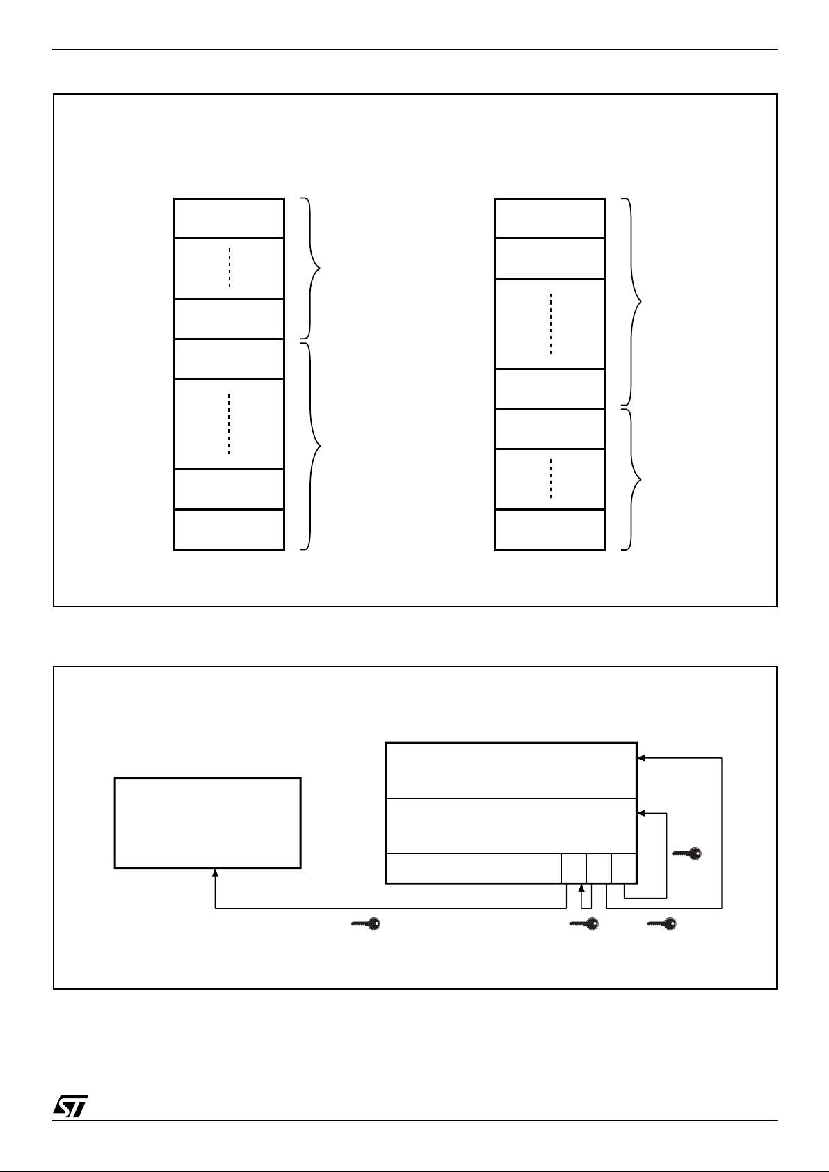
The device features an asymmetrical blocked ar-
chitecture. The M28R400C has an array of 15
blocks: 8 Parameter Blocks of 4 KWord and 7
Main Blocks of 32 KWord. M28R400CT has the
Parameter Blocks at the top of the memory address space while the M28R400CB locates the
Parameter Blocks starting from the bottom. The
memory maps are s hown in Figure 4, Block Addresses.
The M28R400C features an instant, individual
block locking scheme that allo ws any block to be
locked or unlocked with no latency, enabling instant code and data protection. All blocks have
three levels of protection. They can be locked and
locked-down individually preventing any accidental programming or erasure. There is an additional
hardware protection against program and block
erase. When V
PP
≤ V
PPLK
all blocks are p rotected
against program or block erase. All blocks are
locked at power-up.
Each block can be erased separately. Erase can
be suspended in order to perform either read or
program in any other block and then resumed.
Program can be suspended to read data in any
other block and then resumed. Each block can be
programmed and erased over 100,000 cycles.
The device includes a 128 b it Protection Regi ster
and a Security Block to increase the protection of
a system design. The Protection Register is divided into two 64 bit segments, the first one contains
a unique device number writte n by ST, while the
second one is one-time-programm able by the user. The user programmable segm ent can be permanently protected. The Security Block,
parameter block 0, can be perman ently protected
by the user. Figure 5, shows the Security Block
Memory Ma p.
Program and Erase c ommands are written to the
Command Interface of the memory. An on-chip
Program/Erase Controller takes care of the timings necessary for program and erase operations.
The end of a program or erase operation can be
detected and any error conditions identified. The
command set required to control the memory is
consistent with JEDEC standards.
The memory is offered in a TFBGA46 (0.75mm
pitch) package and is supplied with all the bits
erased (set to ’1’).
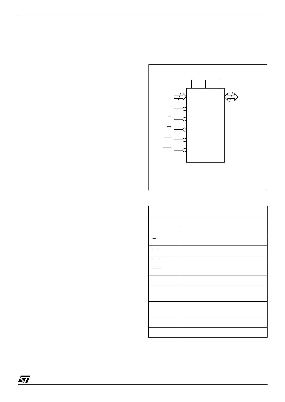
Figure 2. Logic Diagram
Table 1. Signal Names
A0-A17 Address Inputs
DQ0-DQ15 Data Input/Output
E
Chip Enable
G
Output Enable
W
Write Enable
RP
Reset
WP
Write Protect
V
DD
Core Power Supply
V
DDQ
Power Supply for
Input/Output
V
PP
Optional Supply Voltage for
Fast Program & Erase
V
SS
Ground
NC Not Connected Internally
AI04392
18
A0-A17
W
DQ0-DQ15
V
DD
M28R400CT
M28R400CB
E
V
SS
16
G
RP
WP
V
DDQVPP
M28R400CT, M28R400CB
6/50
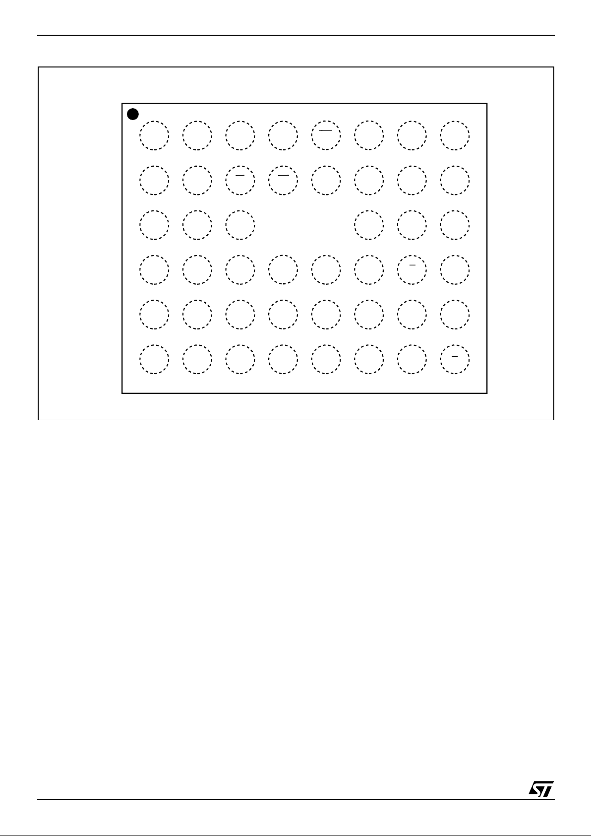
Figure 3. TFBGA Connections (Top view through package)
AI04142
C
B
A
87654321
E
D
F
A4
A7V
PP
A8A11
A13
A0EDQ8DQ5DQ14A16
V
SS
DQ0DQ9DQ3DQ6
DQ15
V
DDQ
DQ1DQ10V
DD
DQ7V
SS
DQ2
A2
A5A17WA10
A14
A1A3A6A9A12A15
RP NC
DQ4
DQ13
G
DQ12
DQ11
WP NC
7/50
M28R400CT, M28R400CB
Figure 4. Block Addresses
Note: Also see Appe ndi x A, Tables 22 and 23 for a f ul l l isting of the B l ock Addresses.
Figure 5. Security Block Memory Map
AI04393
4 KWords
3FFFF
3F000
32 KWords
0FFFF
08000
32 KWords
07FFF
00000
M28R400CT
Top Boot Block Addresses
4 KWords
38FFF
38000
32 KWords
30000
37FFF
Total of 8
4 KWord Blocks
Total of 7
32 KWord Blocks
4 KWords
3FFFF
38000
32 KWords
32 KWords
00FFF
00000
M28R400CB
Bottom Boot Block Addresses
4 KWords
37FFF
0FFFF
32 KWords
30000
08000
Total of 7
32 KWord Blocks
Total of 8
4 KWord Blocks
07FFF
07000
AI03523
Parameter Block # 0
User Programmable OTP
Unique device number
Protection Register Lock 2 1 0
88h
85h
84h
81h
80h

M28R400CT, M28R400CB
8/50
SIGNAL DESCRIPTIONS
See Figure 2 Logic Diagram and Table 1,Signal
Names, for a brief overview of the signals connected to this device.
Address Inputs (A0-A17). The Address Inputs
select the cell s in the memory arra y to access during Bus Read operations. During Bus Write operations they control the commands sent to the
Command Interface of the internal state machine.
Data Input/Output (DQ0-DQ15). The Data I/O
outputs the data stored at the selected address
during a Bus Read operation or inputs a command
or the data to be programmed durin g a Write Bus
operation.
Chip Enable (E
). The Chip Enable input acti-
vates the memory control logic, input buffers, decoders and sense amplifiers. When Chip Enable is
at V
IL
and Reset is at VIH the device is in active
mode. When Chi p E nable is at V
IH
the memory is
deselected, the outputs are high im pedance and
the power consumption is reduced to the stand-by
level.
Output Enable (G
). The Output Enable controls
data outputs during the Bus Read operation of the
memory.
Write Enable (W
). The Write Enable controls the
Bus Write operation of the memory’s Command
Interface. The data and address inputs are latched
on the rising edge of Chip Enable, E, or Write Enable, W
, whichever occurs first.
Write Protect (WP
). Write Protect is an input
that gives an additional hardware protection for
each block. When Write Protect is at V
IL
, the Loc kDown is enabled and the protection status of the
block cannot be changed. When Write Protect is at
V
IH
, the Lock-Down is disabled and the block can
be locked or unlocked. (refer to Table 6, Read Protection Register and Protection Register Lock).
Reset (RP
). The Reset input provides a hard-
ware reset of the mem ory. When Reset is at V
IL
,
the memory is in reset mode: the outputs are high
impedance and the current consumption is minimized. After Reset all blocks are in the Locked
state. When Reset is at V
IH
, the device is in normal
operation. Exiting reset mode the device enters
read array mode, but a negative transition of Chip
Enable or a c hange of the address is require d to
ensure valid data outputs.
V
DD
Supply Vol tag e (1 . 65 V to 2.2V) . V
DD
provides the power supply to the i nternal core of
the memory device. It is the main power supply for
all operations (Read, Program and Erase).
V
DDQ
Supply Voltage (1.65V to 2.2 V). V
DDQ
provides the power supply to the I/O pins and enables all Outputs to be powered independently
from V
DD
. V
DDQ
can be tied to VDD or can use a
separate supply.
V
PP
Program Supply Voltage. VPP is both a
control input and a power supply pin. The two
functions are selected by the voltage range applied to the pin. The Supply Voltage V
DD
and the
Program Supply Voltage V
PP
can be applied in
any order.
If V
PP
is kept in a low voltage range (0V to 3.6V)
V
PP
is seen as a control input. In this case a volt-
age lower than V
PPLK
gives protection against pro-
gram or block erase, while V
PP
> V
PP1
enables
these functions (see Table 14, DC Characteristics
for the relevant values). V
PP
is only sampled at the
beginning of a program or bloc k erase; a change
in its value after the operation has started does not
have any effect and program or erase operations
continue.
If V
PP
is in the range 11.4V to 12.6V it acts as a
power supply pin. In this condition V
PP
must be
stable until the Program/Erase al gorithm is completed (see Table 16 and 17).
V
SS
Ground. VSS is the ref erence for all voltage
measurements.
Note: Each device in a system should have
V
DD, VDDQ
and VPP decoupled with a 0.1µF ca-
pacitor close to the pin. See Figure 7, AC Measurement Load Circu it. The PCB trace widths
should be sufficient to carry the required V
PP
program and erase currents.
9/50
M28R400CT, M28R400CB
BUS OPERATIONS
There are six standard bus operations that control
the device. These are B us Read, Bus Wri te, Output Disable, Standby, Automatic Standby and Reset. See Table 2, Bus Operations, for a summary.
Typically glitches of less than 5ns on Chip Enable
or Write Enable are ignored by the memory and do
not affect bus operations.
Read. Read Bus operations are used to ou tput
the contents of the Memory Array, the Electr onic
Signature, the Status Register and the Common
Flash Interface. Both Chip Enable and Output Enable must be at V
IL
in order to perform a read operation. The Chip Enable in put should b e used to
enable the device. Out put E nable s houl d be us ed
to gate data onto the output. The data read depends on the previous command written to the
memory (see Command Interface section). See
Figure 8, Read Mode AC Wa veforms, and Table
15, Read AC Characteristics, for details of when
the output becomes valid.
Read mode is the default state of the device when
exiting Reset or after power-up.
Write. Bus Write operations write Comm ands to
the memory or latch Input Data to be programmed.
A write operation is initiated when Chip Enable
and Write Enable are at V
IL
with Output Enable at
V
IH
. Commands, Input Data and Addresses are
latched on the rising edge of Write Enable or Chip
Enable, whichever occurs first.
See Figures 9 and 10, Write A C Wav eforms, and
Tables 16 and 17, Write AC Characteristics, for
details of the timing requirements.
Output Disable. The data outputs are high impedance when the Output Enable is at V
IH
.
Standby. S tandby disables m ost of the internal
circuitry allowing a substantial reduction of the current consumption. The memory is in stand-by
when Chip Enable is at V
IH
and the devic e is in
read mode. The power consumption is reduced to
the stand-by level and t he outputs are set to high
impedance, independently from the Output Enable
or Write Enable inputs. If Chip En able switches to
V
IH
during a program or erase operat ion, the de-
vice enters Standby mode when finished.
Automatic Standby. Automatic Standby pro-
vides a low power consumption state during Read
mode. Following a read operation, the device enters Automatic Standby after 150ns of bus inactivity even if Chip Enable is Low, V
IL
, and the supply
current is reduced to I
DD1
. The data Inputs/Outputs will still output data if a bus Read operation is
in progress.
Reset. During Reset mode when Output Enable
is Low, V
IL
, the memory is deselected and the outputs are high impedance. The memory is in Reset
mode when Reset is at V
IL
. The power consumption is reduced to the Standby level, independently
from the Chip Enable, Output Enable or Write Enable inputs. If Reset is pulled to V
SS
during a Program or Erase, this operation is aborted and the
memory content is no longer valid.
Table 2. Bus Operations
Note: X = VIL or VIH, V
PPH
= 12V ± 5%.
Operation E G W RP WP
V
PP
DQ0-DQ15
Bus Read
V
IL
V
IL
V
IH
V
IH
X Don’t Care Data Output
Bus Write
V
IL
V
IH
V
IL
V
IH
X
V
DD
or V
PPH
Data Input
Output Disable
V
IL
V
IH
V
IH
V
IH
X Don’t Care Hi-Z
Standby
V
IH
XX
V
IH
X Don’t Care Hi-Z
Reset X X X
V
IL
X Don’t Care Hi-Z

M28R400CT, M28R400CB
10/50
COMMAND INTERFACE
All Bus Write operations to the memory are in terpreted by the Command Interface. Commands
consist of one or more sequential Bus Write operations. An internal Program/Erase Controller handles all timings and verifies the correct execution
of the Program and Erase commands. The Program/Erase Controller provides a S tatus Register
whose output may be read at any time during, to
monitor the progress of the operation, or t he Program/Erase states. See Appendix D, Table 30,
Write State Machine Current/Next, for a summary
of the Command Interface.
The Command Interface is reset to Read mode
when power is first applied, when exiting from Reset or whenever V
DD
is lower than V
LKO
. Command sequences must be followed exactly. Any
invalid combination of commands will reset the device to Read mode. Refer to Table 3, Commands,
in conjunction with the text descriptions below.
Read Memory Array Command
The Read command returns the memory to its
Read mode. One Bus Write cycle is required to issue the Read Memory Array command and return
the memory to Read mode . Subsequent read operations will read the addressed loc ation and output the data. When a device Reset occurs, the
memory defaults to Read mode.
Read Status Register Command
The Status Register indicates when a program or
erase operation is complete and the success or
failure of the operation itself. Issue a Read Status
Register command to rea d the Status Register’s
contents. Subsequent Bus Read operations read
the Status Register at any address , until another
command is issued. See Table 10, Status Register
Bits, for details on the definitions of the bits.
The Read Status Register command may be issued at any time, even during a Program/Erase
operation. Any Read attempt during a Program/
Erase operation will automatically outp ut the content of the Status Register.
Read Electronic Signature Command
The Read Electronic Signature command reads
the Manufacturer and Device Codes and the Block
Locking Status, or the Protection Register.
The Read Electronic Signature command consists
of one write cycle, a subsequent read will output
the Manufacturer Code, the Device Code, the
Block Lock and Lock-Down Status, or the Protection and Lock Register. See Tables 4, 5 and 6 for
the valid address.
Read CFI Query Command
The Read Query Command is used t o read data
from the Common Flash Interface (CFI ) Memory
Area, allowing programming equipment or appli-
cations to automatically match their interface to
the characteristics of the device. One Bus Write
cycle is required to issue the Read Query Command. Once the command is issued subsequent
Bus Read operations read from the Common
Flash Interface Memory Area. See Appendix B,
Common Flash Inte rface, Tables 2 4, 25, 26, 27,
28 and 29 for details on the information contained
in the Common Flash Interface memory area.
Block Erase Command
The Block Erase c ommand can be used to erase
a block. It sets all the bits within the selected block
to ’1’. A ll previous data in t he block is lost. If t he
block is protected then the Erase operation will
abort, the data in the block will not be changed and
the Status Register will output the error.
Two Bus Write cycles are required to issue the
command.
■ The first bus cycle sets up the Erase command.
■ The second latches the block address in the
internal state machine and starts the Program/
Erase Controller.
If the second bus cycle is not Write Erase Confirm
(D0h), Status Register bits b4 and b5 are s et and
the command aborts.
Erase aborts if Reset turns to V
IL
. As data integrity
cannot be guaranteed when the Erase operation is
aborted, the block must be erased again.
During Erase operations the memory will accept
the Read Status Register com mand and th e Program/Erase Suspend command, all other commands will be ignored. Typical Erase times are
given in Table 7, Program, Erase Times and Program/Erase Endurance Cycles.
See Appendix C, Figure 18, Block Erase Flowchart and Pseudo Code, for a suggested flowchart
for using the Block Erase command.
Chip Erase Command
The Chip Erase command can be used to erase
the entire chip. It sets all of the bits in unprotected
blocks of the memory to ’1’. All previous data is
lost. Two Bus Write operations are requ ired to issue the Chip Erase Command.
■ The first bus cycle sets up the Chip Erase
command.
■ The second confirms the Chip Erase command
and starts the Program/Erase Controller.
The command can be issued to any address. If
any blocks are protec ted then these are ignored
and all the other blocks are erased. If all of the
blocks are protected the Chip Erase op erat i on appears to start but wi ll terminate, leaving the data
unchanged. No error condition is gi ven when protected blocks are ignored.

11/50
M28R400CT, M28R400CB
During the erase o peration th e memory w ill only
accept the Read Status Register command. All
other commands will be ignored, including the
Erase Suspend com mand. It is no t possible to issue any command to abort the operation.
Chip Erase commands should be limited to a maximum of 100 Program/Erase cycles. After 100 Program/Erase cycles the internal algorithm will still
operate properly but some degradation in performance may oc c ur.
Typical chip erase times are given in Table 7.
Program Command
The memory array can be programmed word-byword. Two bus write cycles are required to issue
the Program Command.
■ The first bus cycle sets up the Program
command.
■ The second latches the Address and the Data to
be written and starts the Program/Erase
Controller.
During Program operations the memory will accept the Read Status Register command and the
Program/Erase Suspend command. Typical Program times are given in Tab le 7, P rogram, Erase
Times and Program/Erase Endurance Cycles.
Programming aborts if Res et goes to V
IL
. As data
integrity cannot be guaranteed when the program
operation is aborted, the block containing the
memory location must be erased and reprogrammed.
See Appendix C, Figure 15, Program Flowchart
and Pseudo Code, for t he flowchart for using t he
Program command.
Double Word Program Command
This feature is offered to improve the programming
throughput, writing a page of two adjacent words
in parallel.The two words m ust differ only for the
address A0. Program m ing s hould not be attempted when V
PP
is not at V
PPH
. The command can be
executed if V
PP
is below V
PPH
but the result is not
guaranteed.
Three bus write cycles are necessary to issue the
Double Word Program command.
■ The first bus cycle sets up the Double Word
Program Command.
■ The second bus cycle latches the Address and
the Data of the first word to be written.
■ The third bus cycle latches the Address and the
Data of the second word to be written and starts
the Program/Erase Controller.
Read operations output the Status Register content after the programming has started. Programming aborts if Reset goe s to V
IL
. As data integrity
cannot be guaranteed when the program opera-
tion is aborted, the block containin g the memory
location must be erased and reprogrammed.
See Appendix C, Figure 16, Double Word Program Flowchart and Pseudo Code, for the flowchart for using the Double Word Program
command.
Clear Status Register Command
The Clear Status Register com m and can be used
to reset bits 1, 3, 4 and 5 in the Status Register to
‘0’. One bus write cycle is required to issue the
Clear Status Register command.
The bits in the Status Register do not automatically return to ‘0’ when a new Program or Erase command is issued. The error bits in the Status
Register should be cleared before attempting a
new Program or Erase command.
Program/Erase Suspend Command
The Program/Erase Suspend command is used to
pause a Program or Erase operation. One bus
write cycle is required to issue the Program/Erase
command and pause the Program/Erase controller.
During Program/Erase Suspend the Command Interface will accept the Program/Erase Resume,
Read Array, Read Status Register, Read Electronic Signature and Read CFI Query commands. Additionally, if the suspend operation was Erase then
the Program, Block Lock, Block Lock-Down or
Protection Program commands will also be accepted. The block being erased may be protected
by issuing the Block Protect, Block Lock or Protection Program commands. When the Program/
Erase Resume com mand is issued the operation
will complete. Only the blocks not being erased
may be read or programmed correctly.
During a Program/Erase Suspend, the device can
be placed in a pseudo-standby mode by taking
Chip Ena ble to V
IH
. Program/Erase is aborted if
Reset turns to V
IL
.
See Appendix C, Figure 17 , Program Suspend &
Resume Flowchart and Pseudo Code, and Figure
19, Erase Suspend & Resume Flowchart and
Pseudo Code for flowcharts for using the Program/
Erase Suspend command.
Program/Er ase Resu me Command
The Program/Erase Resume command can be
used to restart the Program/Erase Controller after
a Program/Erase Suspend operation has paused
it. One Bus Write cycle is required to issue the
command. Once the command is issued subsequent Bus Read operations read the Status Register.
See Appendix C, Figure 17 , Program Suspend &
Resume Flowchart and Pseudo Code, and Figure
19, Erase Suspend & Resume Flowchart and

M28R400CT, M28R400CB
12/50
Pseudo Code for flowcharts for using the Program/
Erase Resume command.
Prot ection Register Program Command
The Protection Register Program command is
used to Program the 64 bit user One-Time-Programmable (OTP) segment of the Protection Register. The segment is programmed 16 bits at a
time. When shipped all bits in the segment are set
to ‘1’. The user can only program the bits to ‘0’.
Two write cycles are required to issue the Pro tec-
tion Register Program command.
■ The first bus cycle sets up the Protection
Register Program command.
■ The second latches the Address and the Data to
be written to the Protection Register and starts
the Program/Erase Controller.
Read operations output the Status Register content after the programming has started.
The segment can be protected by programming bit
1 of the Protection Lock Register. Bit 1 of the Protection Lock Register protects bit 2 of the Protection Lock Register. Programming bit 2 of the
Protection Lock Register will result in a permanent
protection of the Security Block (see Figure 5, Security Block Memory Map). Attempting to program
a previously protected Protection Register will result in a Status Register error. The protection of
the Protection Register a nd/or the Security Block
is not reversible.
The Protection Register Program cannot be suspended. See Appendix C, Figure 21, Protection
Register Program Flowchart and Pseudo Code,
for the flowchart for using th e Protection Regi ster
Program command.
Block Lock Command
The Block Lock command is used to lock a block
and prevent Program or Erase operations from
changing the data in it. All blocks are locked at
power-up or reset.
Two Bus Write cycles are required to issue the
Block Lock command.
■ The first bus cycle sets up the Block Lock
command.
■ The second Bus Write cycle latches the block
address.
The lock status c an be monitored for eac h block
using the Read Electronic Signature command.
Table. 9 shows the protection status after issuing
a Block Lock command.
The Block Lock bit s are volatile, once set they remain set until a hardware reset or power-down/
power-up. They are cleared by a Blocks Unlock
command. Refer to the section, Block Locking, for
a detailed explanation.
Block Unlock Command
The Blocks Unlock comm and is used to unlock a
block, allowing the block to be programmed or
erased. Two Bus Write cy cles are required to issue the Blocks Unlock command.
■ The first bus cycle sets up the Block Unlock
command.
■ The second Bus Write cycle latches the block
address.
The lock status c an be monitored for eac h block
using the Read Electronic Signature command.
Table. 9 shows the protection status after issuing
a Block Unlock command. Refer to the section,
Block Locking, for a detailed explanation.
Block Lock-Down Command
A locked block cannot be Programmed or Erased,
or have its protection status changed wh en WP
is
low, V
IL
. When WP is high, V
IH,
the Lock-Down
function is disabled and the locked bloc ks can be
individually unlocked by the Block Unlock command.
Two Bus Write cycles are required to issue the
Block Lock-Down command.
■ The first bus cycle sets up the Block Lock
command.
■ The second Bus Write cycle latches the block
address.
The lock status c an be monitored for eac h block
using the Read Electronic Signature command.
Locked-Down blocks revert to the locked (and not
locked-down) state when the device is reset on
power-down. Table. 9 shows the protection status
after issuing a Block Lock-Down co mmand. Refer
to the section, Block Locking, for a detailed explanation.
13/50
M28R400CT, M28R400CB
Table 3. Commands
Note: 1. X = Don’t Care.
2. The signature addresses ar e l i st ed in Tables 4, 5 and 6.
3. Addr 1 and Addr 2 must be consecu tive Addres ses differ i ng only for A0.
Commands
No. of
Cycles
Bus Write Operations
1st Cycle 2nd Cycle 3nd Cycle
Bus
Op.
Addr Data
Bus
Op.
Addr Data
Bus
Op.
Addr Data
Read Memory Array 1+ Write X FFh
Read
Read
Addr
Data
Read Status Register 1+ Write X 70h
Read
X
Status
Register
Read Electronic Signature 1+ Write X 90h
Read
Signature
Addr
(2)
Signature
Read CFI Query 1+ Write 55h 98h Read CFI Addr Query
Block Erase 2 Write X 20h Write
Block
Addr
D0h
Chip Erase 2 Write X 80h Write X D0h
Program 2 Write X
40h or
10h
Write Addr
Data
Input
Double Word Pr ogram
(3)
3 Write X 30h Write Addr 1
Data
Input
Write Addr 2
Data
Input
Clear Status Register 1 Write X 50h
Program/E rase Suspend 1 W rite X B 0h
Program/Erase Resume 1 Wr ite X D0h
Block Lock 2 Write X 60h Write
Block
Address
01h
Block Unlock 2 Write X 60h Write
Block
Address
D0h
Block Lock-Down 2 Write X 60h Write
Block
Address
2Fh
Protection Register
Program
2 Write X C0h Write
Address
Data
Input
M28R400CT, M28R400CB
14/50
Table 4. Read Electronic Signature
Note: RP = VIH.
Table 5. Read Block Lock Signature
Note: 1. A Lo ck ed-Down Block can be locked "DQ0 = 1" or unlock ed "DQ0 = 0"; see Block Lock i ng section.
Table 6. Read Protection Register and Lock Register
Code Device E G W A0 A1 A2-A7 A8-A17 D Q0-DQ7 DQ8-DQ15
Manufacture.
Code
V
IL
V
IL
V
IH
V
IL
V
IL
0 Don’t Care 20h 00h
Device Code
M28R400CT
V
IL
V
IL
V
IH
V
IH
V
IL
0 Don’t Care 2Ah 88h
M28R400CB
V
IL
V
IL
V
IH
V
IH
V
IL
0 Don’t Care 2Bh 88h
Block Status E
G W A0 A1 A2-A7 A8-A11 A12-A17 DQ0 DQ1 DQ2-DQ15
Locked Block
V
IL
V
IL
V
IHVIL
V
IH
0 Don’t Care Block Address 1 0 00h
Unlocked Block
V
IL
V
IL
V
IHVIL
V
IH
0 Don’t Care Block Address 0 0 00h
Locked-Down
Block
V
IL
V
IL
V
IHVIL
V
IH
0 Don’t Care Block Address
X
(1)
1 00h
Word E
G W A0-A7 A8-A17 DQ0 DQ1 DQ2 DQ3-DQ7 DQ8-DQ15
Lock
V
IL
VILV
IH
80h Don’t Care 0
OTP Prot.
data
Security
prot. data
00h 00h
Unique ID 0
V
IL
VILV
IH
81h Don’t Care ID data ID data ID data ID data ID data
Unique ID 1
V
IL
VILV
IH
82h Don’t Care ID data ID data ID data ID data ID data
Unique ID 2
V
IL
VILV
IH
83h Don’t Care ID data ID data ID data ID data ID data
Unique ID 3
V
IL
VILV
IH
84h Don’t Care ID data ID data ID data ID data ID data
OTP 0
V
IL
VILV
IH
85h Don’t Care OTP data OTP data OTP data OTP data OTP data
OTP 1
V
IL
VILV
IH
86h Don’t Care OTP data OTP data OTP data OTP data OTP data
OTP 2
V
IL
VILV
IH
87h Don’t Care OTP data OTP data OTP data OTP data OTP data
OTP 3
V
IL
VILV
IH
88h Don’t Care OTP data OTP data OTP data OTP data OTP data
15/50
M28R400CT, M28R400CB
Table 7. Program, Erase Times and Program/Erase Endura nce Cycles
Parameter Test Conditions
M28R400C
Unit
Min Typ Max
Word Program
V
PP
= V
DD
10 200 µs
Double Word Program
V
PP
= 12V ±5%
10 200 µs
Main Block Program
V
PP
= 12V ±5%
0.16 5 s
V
PP
= V
DD
0.32 5 s
Parameter Block Program
V
PP
= 12V ±5%
0.02 4 s
V
PP
= V
DD
0.04 4 s
Main Block Erase
V
PP
= 12V ±5%
110 s
V
PP
= V
DD
110 s
Chip Erase (preprogrammed)
V
PP
= 12V ±5%
210 s
V
PP
= V
DD
210 s
Chip Program
V
PP
= 12V ±5%
1.25 s
V
PP
= V
DD
25 s
Parameter Block Erase
V
PP
= 12V ±5%
0.8 10 s
V
PP
= V
DD
0.8 10 s
Program/Erase Cycles (per Block) 100,000 cycles
 Loading...