

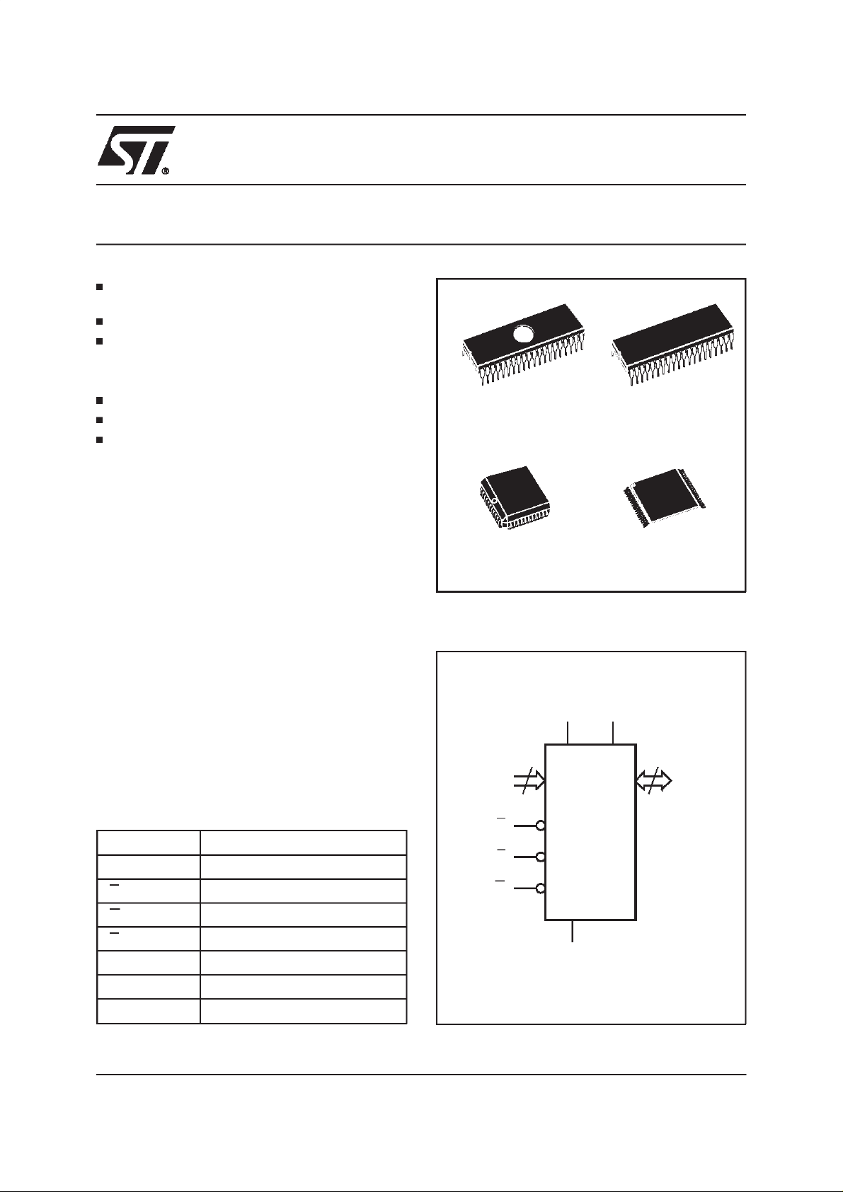
1 Mbit (64Kb x16) UV EPROM and OTP EPROM
5V ± 10%SUPPLYVOLTAGEin READ
OPERATION
FASTACCESSTIME: 35ns
LOW POWERCONSUMPTION:
– Active Current 35mAat 5MHz
– StandbyCurrent 100µA
PROGRAMMINGVOLTAGE:12.75V ± 0.25V
PROGRAMMINGTIME: 100µs/byte (typical)
ELECTRONICSIGNATURE
– ManufacturerCode: 0020h
– Device Code: 008Ch
DESCRIPTION
The M27C1024 is a 1 MbitEPROM offered in the
two ranges UV (ultra violet erase) and OTP (one
time programmable). It is ideally suited for microprocessorsystemsrequiringlargedata or program
storage and is organized as 65,536 words of 16
bits.
The FDIP40W(window ceramic frit-seal package)
has a transparent lid which allows the user to
expose the chip to ultraviolet light to erase the bit
pattern. A new pattern can then be written to the
deviceby followingthe programming procedure.
For application where the content is programmed
only one time and erasure is not required, the
M27C1024 is offered in PDIP40, PLCC44 and
TSOP40(10 x 14mm) packages.
40
1
FDIP40W (F)
PLCC44 (C) TSOP40 (N)
Figure1. Logic Diagram
V
CC
16
A0-A15
M27C1024
40
1
PDIP40 (B)
10 x 14mm
V
PP
16
Q0-Q15
Table1. Signal Names
A0-A15 Address Inputs
Q0-Q15 Data Outputs
E Chip Enable
G Output Enable
P Program
V
PP
V
CC
V
SS
September 1998 1/15
Program Supply
Supply Voltage
Ground
P
E
G
M27C1024
V
SS
AI00702B
M27C1024
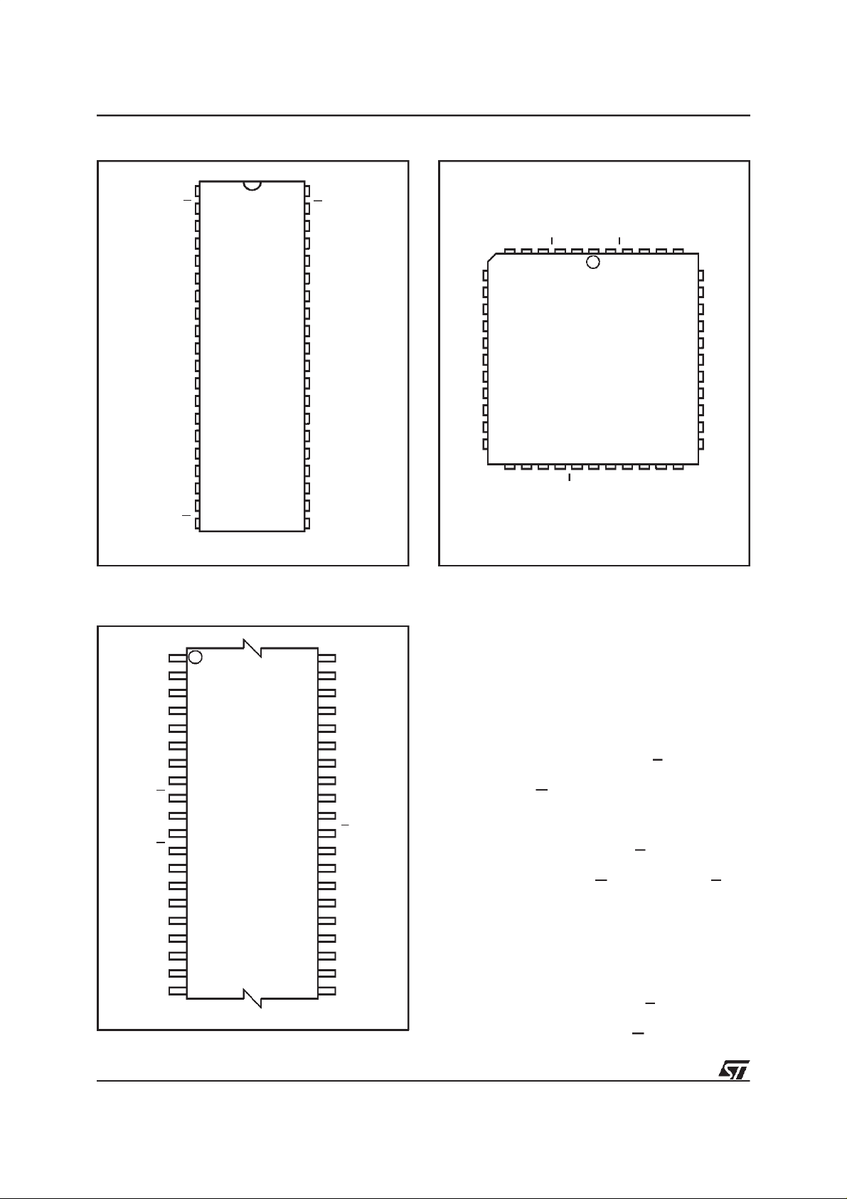
Figure2A. DIP Pin Connections
V
PP
Q15
Q14
Q13
Q12
Q11
Q10
Q9
Q8
V
SS
Q7
Q6
Q5
Q4
Q3
Q2
Q0
1
2
3
4
5
6
7
8
9
10
M27C1024
11
12
13
14
15
16
17
18
19
40
39
38
37
36
35
34
33
32
31
30
29
28
27
26
25
24
23
22
2120
AI00703
V
CC
PE
NC
A15
A14
A13
A12
A11
A10
A9
V
SS
A8
A7
A6
A5
A4
A3
A2Q1
A1
A0G
Figure2B. LCC Pin Connections
Q15
Q13
Q14
Q12
Q11
Q10
Q9 A10
Q8
V
SS
NC
Q6
Q5
Q4
12
Q3
Q2
M27C1024
Q1
Q0
CC
NC
VPPE
V
1
44
23
G
A0
NC
P
A1
NC
A2
A15
A3
A14
34
A4
A13
A12
A11
A9
V
SS
NC
A8Q7
A7
A6
A5
AI00704
Warning: NC = Not Connected.
Figure2C. TSOPPin Connections
A9
1
A10
A11
A12 A6
A13 A5
A14
A15
NC
P
V
CC
V
DQ15
DQ14
DQ13
DQ12 DQ4
DQ11 DQ5
DQ10
DQ9
DQ8
Warning: NC = Not Connected.
10
11
PP
E
20 21
M27C1024
(Normal)
40
31
30
AI01582
V
SS
A8
A7
A4
A3
A2
A1
A0
G
DQ0
DQ1
DQ2
DQ3
DQ6
DQ7
V
SS
Warning: NC = Not Connected.
DEVICEOPERATION
The modes of operations of the M27C1024 are
listedin theOperatingModestable.Asingle power
supplyis required in the read mode. All inputsare
TTL levels except for Vpp and 12V on A9 for
ElectronicSignature.
Read Mode
The M27C1024 has two control functions,both of
which must be logically active in order to obtain
data at the outputs. Chip Enable(E) is the power
control and should be used for device selection.
OutputEnable(G) is the outputcontroland should
be used to gate data to the output pins, independent of device selection. Assuming that the
addresses are stable, the address access time
)isequaltothedelayfromEtooutput(t
(t
AVQV
Data is available at the output after a delayof t
ELQV
OE
from the falling edge of G, assuming that E has
been low and the addresses have been stable for
at least t
AVQV-tGLQV
.
StandbyMode
The M27C1024 has a standby mode which reducestheactive current from 35mAto 100µA.
The M27C1024 is placed in the standby mode by
applyinga TTLhigh signal to theE input. When in
thestandbymode, theoutputsare ina highimpedance state,independentof the G input.
).
2/15
M27C1024
Table2. AbsoluteMaximum Ratings
(1)
Symbol Parameter Value Unit
T
A
T
BIAS
T
STG
V
IO
V
CC
V
A9
V
PP
Notes: 1. Except for therating ”Operating Temperature Range”, stresses above those listed in the Table ”AbsoluteMaximum Ratings”
2. Minimum DC voltage on Input or Output is –0.5V with possible undershoot to –2.0V for a periodlessthan 20ns. Maximum DC
3. Depends on range.
Ambient Operating Temperature
Temperature Under Bias –50 to125
Storage Temperature –65 to150 °C
(2)
Input or Output Voltages (except A9) –2 to7 V
Supply Voltage –2 to7 V
(2)
A9 Voltage –2 to13.5 V
Program Supply Voltage –2 to14 V
may cause permanentdamage to thedevice. These are stress ratings only and operationof the device at these or any other
conditions above those indicated in the Operating sections of this specification is not implied.Exposure to Absolute Maximum
Rating conditions for extended periods may affect device reliability.Refer also to the STMicroelectronics SURE Program and other
relevant qualitydocuments.
voltage on Output is V
+0.5Vwith possible overshoot toVCC+2V for a periodless than 20ns.
CC
(3)
–40 to125 °C
°
C
Table3. Operating Modes
Mode E G P A9 V
Read V
Output Disable V
Program V
Verify V
Program Inhibit V
Standby V
Electronic Signature V
Note: X= VIHor VIL,VID= 12V ±0.5V
PP
IL
IL
IL
IL
IH
IH
IL
V
IL
V
IH
XV
V
IL
XXXVPPHi-Z
XXXV
V
IL
V
IH
XXV
Pulse X V
IL
V
IH
V
IH
XV
CC
CC
or V
or V
PP
SS
SS
XVPPData Output
or V
CC
SS
V
ID
V
CC
Q0 - Q15
Data Output
Hi-Z
Data Input
Hi-Z
Codes
Table4. ElectronicSignature
Identifier A0 Q7 Q6 Q5 Q4 Q3 Q2 Q1 Q0 Hex Data
Manufacturer’s Code V
Device Code V
Note: Outputs Q8-Q15 are set to ’0’.
IL
IH
00100000 20h
100011008Ch
3/15
M27C1024
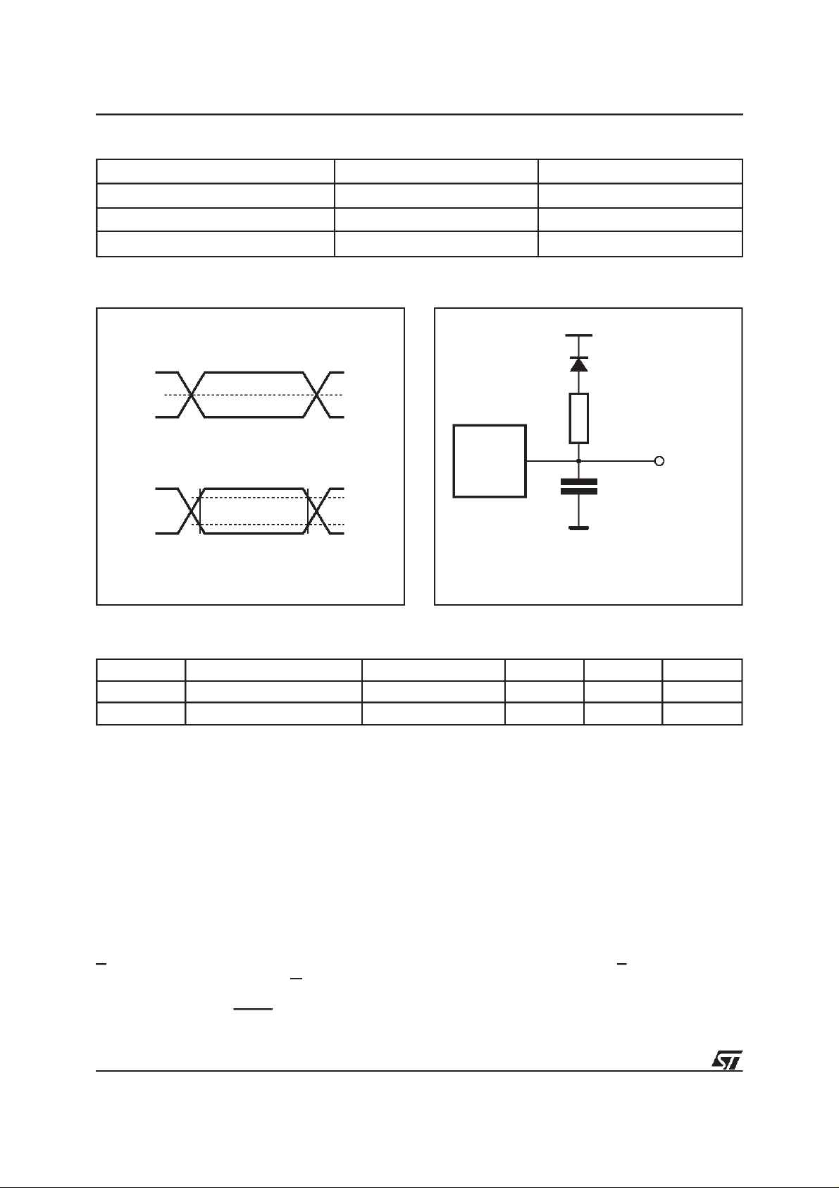
Table5. AC Measurement Conditions
High Speed Standard
Input Rise and Fall Times
Input Pulse Voltages 0 to 3V 0.4V to 2.4V
Input and Output Timing Ref. Voltages 1.5V 0.8V and 2V
≤
10ns
≤
20ns
Figure3. AC TestingInput Output Waveform
High Speed
3V
1.5V
0V
Standard
2.4V
0.4V
Table6. Capacitance
Symbol Parameter Test Condition Min Max Unit
C
IN
C
OUT
Note: 1. Sampled only, not 100% tested.
Input Capacitance VIN=0V 6 pF
Output Capacitance V
(1)
(TA=25°C, f = 1 MHz)
2.0V
0.8V
AI01822
Figure4. AC TestingLoad Circuit
1.3V
1N914
3.3kΩ
DEVICE
UNDER
TEST
C
L
CL= 30pF for High Speed
CL= 100pF for Standard
CLincludes JIGcapacitance
=0V 12 pF
OUT
OUT
AI01823B
Two Line Output Control
BecauseEPROMs areusuallyusedinlargermemory arrays, this product features a 2 line control
functionwhich accommodates the use of multiple
memory connection. The two line control function
allows:
a. the lowest possiblememory powerdissipation,
b. complete assurancethat output bus contention
will not occur.
Forthemostefficientuseofthesetwocontrollines,
E should be decoded and used as the primary
deviceselectingfunction,whileG should be made
a common connection to all devices in the array
and connected to the READline from the system
4/15
controlbus.Thisensuresthat all deselectedmemory devices are in their low power standby mode
and that the output pins are only active when data
is requiredfrom a particular memory device.
SystemConsiderations
The power switching characteristics of Advanced
CMOSEPROMs require careful decoupling of the
devices. The supply current, I
, has three seg-
CC
mentsthat are of interestto the system designer :
the standby current level, the active current level,
and transient current peaks that are producedby
thefalling and rising edges ofE. Themagnitudeof
transientcurrentpeaksisdependentonthecapacitive and inductive loading of the device at the
output.
M27C1024
Table7. Read Mode DC Characteristics
(1)
(TA=0 to 70 °C, –40 to 85 °C; –40 to 105 °C or –40 to 125 °C; VCC=5V±5% or 5V ± 10%; VPP=VCC)
Symbol Parameter Test Condition Min Max Unit
I
LI
I
LO
I
CC
I
CC1
I
CC2
I
PP
V
IL
V
IH
V
OL
V
OH
Notes: 1. VCCmust be applied simultaneouslywith or before VPPand removed simultaneously with or afterV
2. Maximum DC voltage on Output is VCC+0.5V.
Input Leakage Current 0V ≤ VIN≤ V
Output Leakage Current 0V≤V
Supply Current
E=V
= 0mA, f = 5MHz
I
OUT
Supply Current (Standby) TTL E= V
≤
OUT
,G=VIL,
IL
IH
CC
V
CC
Supply Current (Standby) CMOS E > VCC–0.2V 100 µA
Program Current VPP=V
CC
Input Low Voltage –0.3 0.8 V
(2)
Input High Voltage 2 VCC+1 V
Output Low Voltage IOL= 2.1mA 0.4 V
Output High VoltageTTL IOH= –400µA 2.4 V
Output High VoltageCMOS I
= –100µAV
OH
CC
– 0.7 V
PP.
±10 µA
10
±
A
µ
35 mA
1mA
100
A
µ
Table8A. ReadModeAC Characteristics
(1)
(TA=0 to 70 °C, –40 to 85 °C; –40 to 105 °C or –40 to 125 °C; VCC=5V±5% or 5V ± 10%; VPP=VCC)
M27C1024
Symbol Alt Parameter Test Condition
-35
(3)
-45
Min Max Min Max Min Max
t
t
AVQV
t
ELQV
t
GLQV
(2)
t
EHQZ
(2)
t
GHQZ
t
AXQX
Notes: 1. VCCmust be applied simultaneouslywith or before VPPand removed simultaneously with or afterV
2. Sampled only, not 100% tested.
3. Speed obtainedwith High Speed AC measurementconditions.
Address Valid to Output Valid E = VIL,G=V
ACC
tCEChip Enable Low to Output Valid G = V
tOEOutput Enable Low to Output Valid E = V
tDFChip Enable High to Output Hi-Z G = V
tDFOutput Enable High to Output Hi-Z E = V
Address Transition to Output
t
OH
Transition
E=V
,G=VIL000ns
IL
IL
IL
IL
IL
IL
35 45 55 ns
35 45 55 ns
20 25 30 ns
030030030ns
030030030ns
(3)
PP.
-55
Unit
(3)
5/15
 Loading...