

SGS Thomson Microelectronics M27512 Datasheet
FA ST ACCESS TIME: 200ns
EXTENDED TEMPERATURE RANGE
SINGLE 5V SUPPLY VOLTAGE
LOW STANDBY CURRE NT: 40mA max
M27512
NMOS 512K (64K x 8) UV EPROM
TTL COMPATIBLE DURING READ and
PROGRAM
FAST PROGRAMMING ALGORITHM
ELECTRONIC SIGNATURE
PROGRAMMING VOLTAGE: 12V
DESCRIPTION
The M27512 is a 524,288 bit UV erasable and
electrically programmable memory EPROM. It is
organized as 65,536 words by 8 bits.
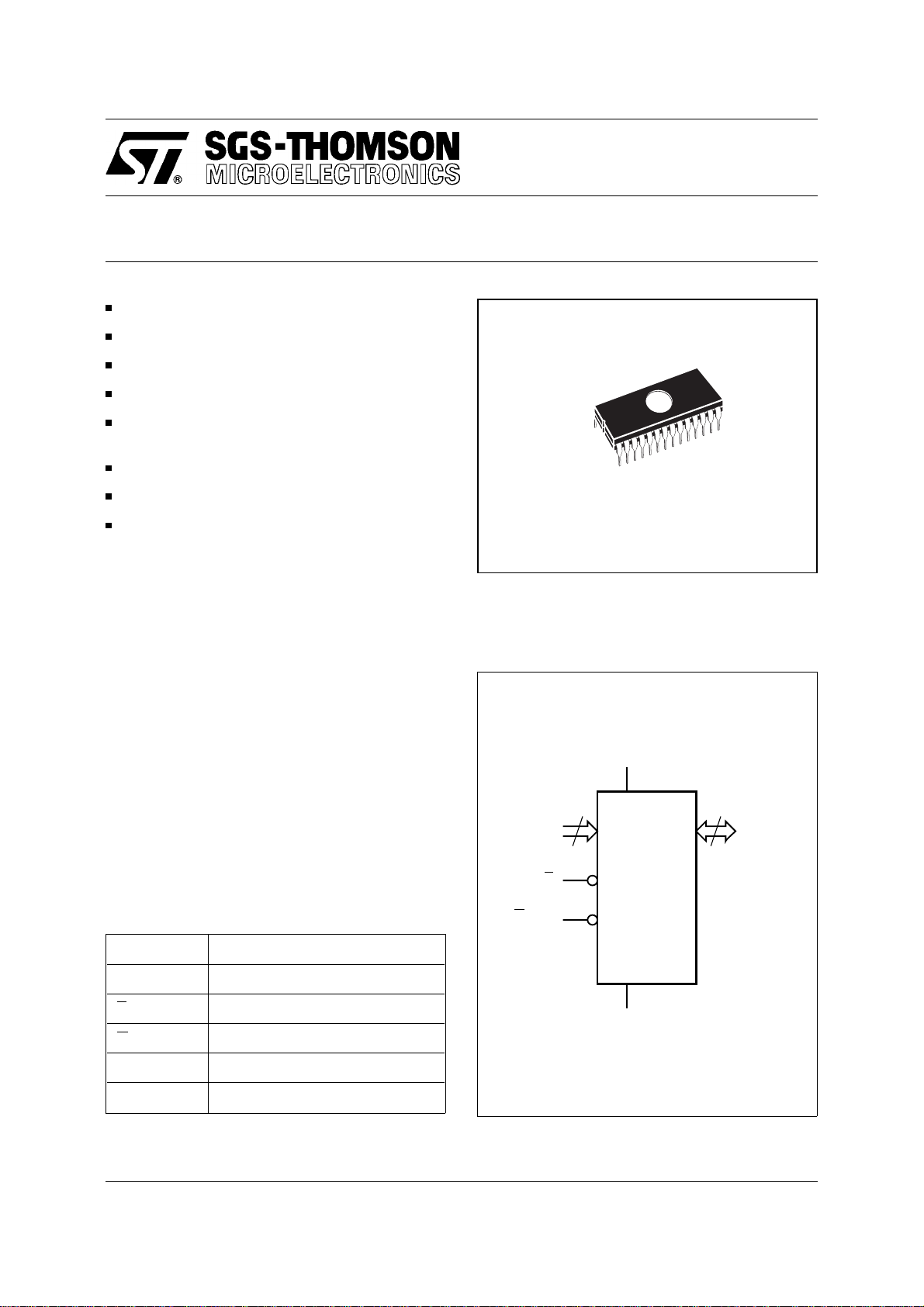
The M27512 is housed in a 28 Pin Window Ceramic
Frit-Seal Dual-in-Line pac kage. The transparent lid
allows the user to expose the chip t o ultraviolet light
to erase the bit patt ern. A new pattern can then be
written to the devic e by following t he programmi ng
procedure.
28
1
FDIP28W (F)
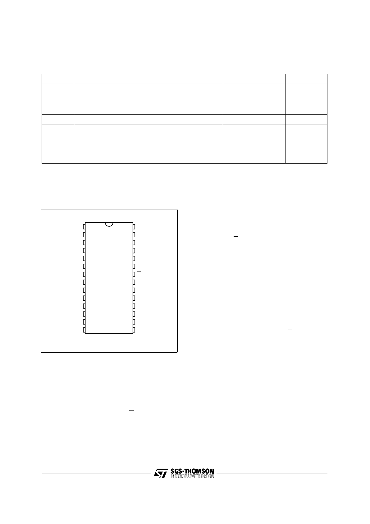
Figure 1. Logic Diag ra m
V
CC
16
A0-A15
8
Q0-Q7
E
Table 1. Signal Names
A0 - A15 Address Inputs
Q0 - Q7 Data Outputs
E Chip Enable
GV
PP
V
CC
V
SS
March 1995 1/11
Output Enable / Program Supply
Supply Voltage
Ground
GV
PP
M27512
V
SS
AI00765B
M27512
Tab le 2. Absol ute Maxim u m Ratin gs
Symbol Parameter Value Unit
T
A
T
BIAS
T
STG
V
IO
V
CC
V
A9
V
PP
Note: Except for the rating "Operating T emperature R ange", stresses above those lis ted in the Table "Absolute Maximum Ratings" may cause
permanent damage to the device. These are stress ratings only and opera tion of the device at these or any other conditions above those
indicated in the Operating sections of this specification is not implied. Exposure to Absolute Maximum Rati ng conditions for extended periods
may affect device reliabil ity. Refer also to the SGS-THOMSON SURE Program and other relevant quality document
Ambient Operating T empera ture
Temperature Under Bias
Storage Temperature –65 to 125 °C
Input or Output Voltages –0.6 to 6.5 V
Supply Voltage –0.6 to 6.5 V
A9 Voltage –0.6 to 13.5 V
Program Supply –0.6 to 14 V
Grade 1
Grade 6
Grade 1
Grade 6
0 to 70
–40 to 85
–10 to 80
–50 to 95
°C
°C
Figure 2. DIP Pin Connect ion s
A15 V
1
A12
2
3
A7
4
A6
5
A5
6
A4
7
A3
A2
A1
A0
Q0
Q2
SS
8
9
10
11
12
13
14
M27512
28
27
26
25
24
23
22
21
20
19
18
17
16
15
AI00766
CC
A14
A13
A8
A9
A11
GV
A10
E
Q7
Q6
Q5Q1
Q4
Q3V
PP
DEVICE OPERATION
The six modes of operations of the M27512 are
listed in the Operating Modes table. A single 5V
power supply is required in the read mode. All
inputs are TTL levels except for
GVPP and 12V on
A9 for Electronic Signature.
Read Mode
The M27512 has two control functions, both of
which must be logically active in order to obtain
data at the outputs. Chip Enable (
E) is the power
control and should be used for device selection.
Output Enable (
G) is the output control and should
be used to gate data to the output pins, independent of device selection. Assuming that the
addresses are s table, addres s access time (t
is equal to the delay from
E to output (t
is available at the out puts after delay of t
the falling edge of
G, assuming that E has been low
ELQV
GLQV
AVQV
). Data
from
and the addresses have been stable for at least
t
AVQ V-tGLQV
.
Stand by Mod e
The M27512 has a standby mode which reduces
the maximum active power current f rom 125mA to
40mA. The M27512 is placed in the standby mode
by applying a TTL high signal to the
E input. Whe n
in the standby mode, the outputs are in a high
impedance state, independent of the
GVPP input.
Two Line Output Control
Because EPROM s are usually used in larger memory arrays, the product features a 2 line control
function which accommodates the use of multiple
memory connection. The two line control function
allows :
a. the lowest possible m emory power dissipation,
b. complete assurance that output bus content i on
will not occur.
)
2/11

M27512
DEVICE OPER ATION (cont’d)
For the most efficient us e of these two control lines,
E should be decoded and used as the primary
device selecting function, while
GVPP should be
made a common connection to all devices in the
array and connected to the
READ line from the
system control bus. This ensures that all deselected memory devices are in their low power
standby mode and that the output pins are only
active when data is r equired from a particular memory device.
System Considerati ons
The power switching characteristics of fast
EPROMs require careful decoupling of the devices.
The supply current, I
, has three segments that
CC
are of interest to t he system designer : the s tandby
current level, the active c urrent level, and transient
current peaks that are produced by the falling and
rising edges of
E. The magnitude of the transient
current peaks is dependent on the capacitive and
inductive loading of the device at the output. The
associated transient voltage peaks can be suppressed by complying with the two line output
control and by properly selected decoupling capacitors. It is recommenced that a 1µF ceramic
capacitor be used on every device between V
CC
and VSS. This should be a high frequency capacitor
of low inherent inductance and should be placed
as close to the device as possible. In addition, a
4.7µF bulk electrolytic capacitor should be used
between V
and VSS for every eight devices. The
CC
bulk capacitor should be located near the power
supply connection point. The purpose of the bulk
capacitor is to overcome the voltage drop caused
by the inductive effects of PCB trac es.
Programming
When delivered, and after each erasure, all bits of
the M27512 are in the “1" state. Data is introduced
by selectively programming ”0s" into the desired bit
locations. Although only “0s” will be programmed,
both “1s” and “0s” can be present in the dat a word.
The only way to change a “0" to a ”1" is by ultraviolet
light erasure. The M27512 is in the programming
mode when
GVPP input is at 12.5V and E is at
TTL-low. The data to be programmed is applied 8
bits in parallel to the data output pins. The levels
required for the address and data inputs are TTL.
The M27512 can use P RESTO Program ming Algorithm that drastically reduces the programming
time (typically less than 50 seconds). Nevertheless
to achieve compatibility with all programming
equipment, the standard Fast Programming Algorithm may also be used.
Fast Programmi ng Al gor ithm
Fast Programming Algorithm rapidly programs
M27512 EPROMs using an efficient and reliable
method suited to the production programming environment. Programming reliability is also ensured
as the incremental program margin of each byte is
continually monitored to determine when it has
been successfully programmed. A flowchart of the
M27512 Fast Programming Algorithm is shown in
Figure 8.
Table 3. Operating Modes
Mode E GV
Read V
Output Disable V
Program V
Verify V
Program Inhibit V
Standby V
Electronic Signature V
Note: X = VIH or VIL, VID = 12V ± 0.5%.
IL
IL
Pulse V
IL
IH
IH
IH
IL
PP
V
IL
V
IH
PP
V
IL
V
PP
X X Hi-Z
V
IL
A9 Q0 - Q7
X Data Out
X Hi-Z
X Data In
X Data Out
X Hi-Z
V
ID
T ab le 4. Electron ic Sig natu r e
Identifier A0 Q7 Q6 Q5 Q4 Q3 Q2 Q1 Q0 Hex Data
Manufacturer’s Code V
Device Code V
IL
IH
00100000 20h
00001101 0Dh
Codes
3/11
M27512
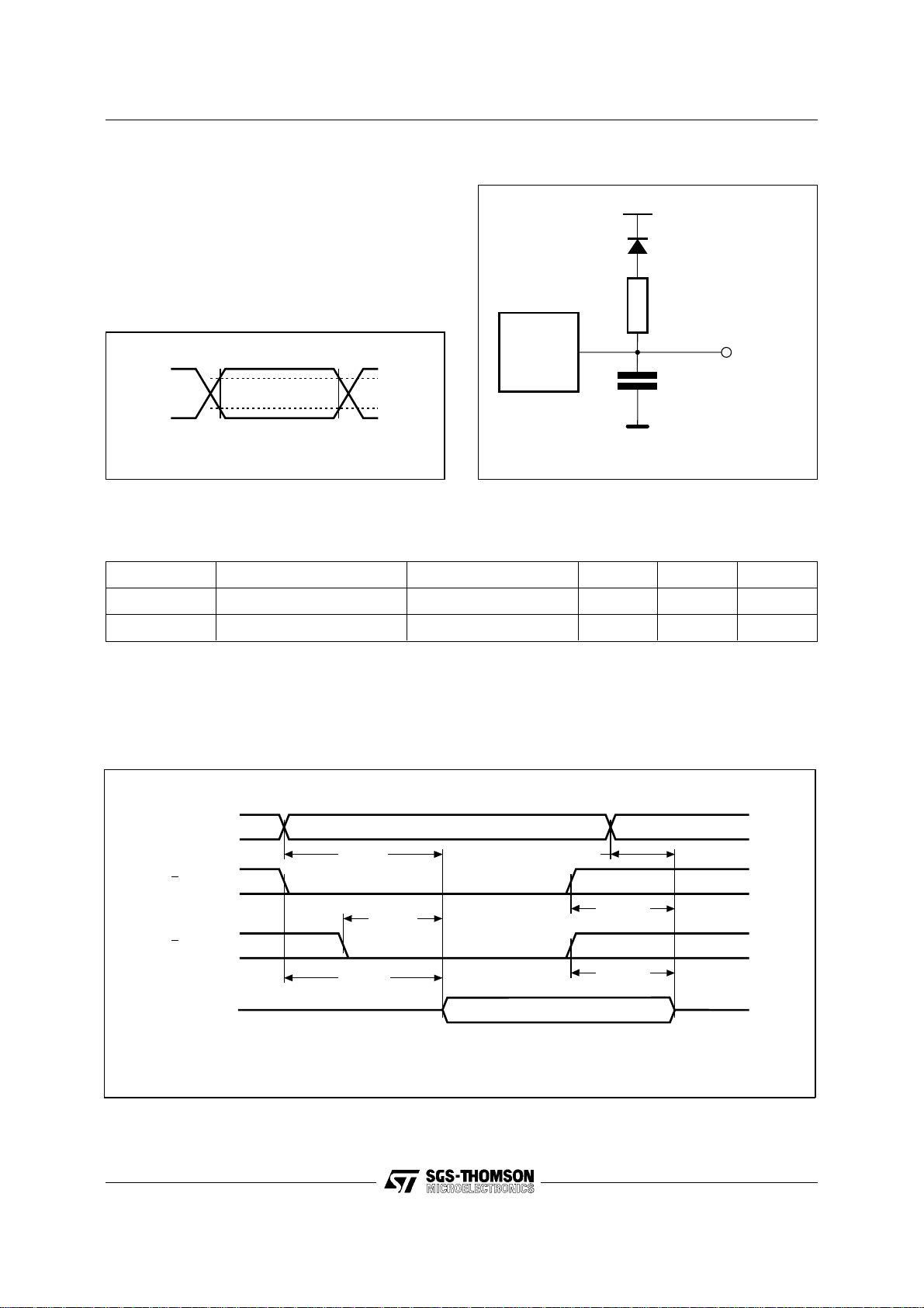
AC MEASUREMENT CONDITIONS
Input Rise and Fall Times ≤ 20ns
Figure 4. AC T esti ng Load Circui t
1.3V
Input Pulse Voltages 0.45V to 2.4V
Input and Output Timing Ref. Voltages 0.8V to 2.0V
1N914
Note that Output Hi-Z is defined as the point where data
is no longer driven.
Figure 3. AC Test ing Input Outp ut W avefo rm s
3.3kΩ
DEVICE
UNDER
2.4V
0.45V
T ab le 5. Capacitance
(1)
(TA = 25 °C, f = 1 MHz )
2.0V
0.8V
AI00827
Symbol Parameter Test Condition Min Max Unit
C
IN
C
OUT
Note: 1. Sampled only, not 100% tested.
Input Capacitance VIN = 0V 6 pF
Output Capacitance V
OUT
TEST
CL = 100pF
CL includes JIG capacitance
= 0V 12 pF
OUT
AI00828
Figure 5. Read Mode AC W aveforms
A0-A15
tAVQV
E
G
tELQV
Q0-Q7
4/11
tGLQV
VALID
tAXQX
tEHQZ
tGHQZ
Hi-Z
DATA OUT
AI00735
 Loading...