

SGS Thomson Microelectronics M2732A-20F6, M2732A-20F1, M2732A-F6, M2732A-F1, M2732A-4F1 Datasheet
...
AI00780B
12
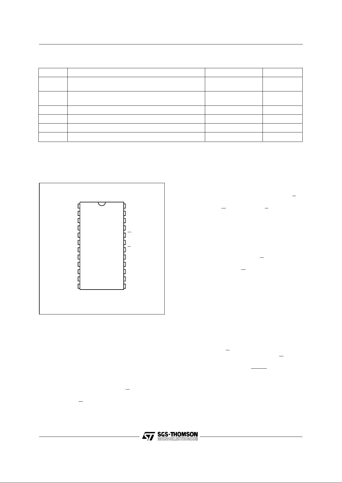
A0-A11 Q0-Q7
V
CC
M2732A
GV
PP
E
V
SS
8
Figure 1. Logic Diag ra m
M2732A
NMOS 32K (4K x 8) UV EPROM
FA ST ACCESS TIME: 200ns
EXTENDED TEMPERATURE RANGE
SINGLE 5V SUPPLY VOLTAGE
LOW STANDBY CURRE NT: 35mA max
INPUTS and OUTP UT S TT L CO MPATIB LE
DURING REA D a n d PRO GR AM
COM P LETELY STATIC
DESCRIP TION
The M2732A is a 32,768 bit UV erasable and
electrically programmable memory EPROM. It is
organized as 4,0 96 words by 8 bit s. The M2732A
with its single 5V pow er supply an d with an acc ess
time of 200 ns, is ideal suited for applications wher e
fast turn around and pattern experimentation one
important requirements.
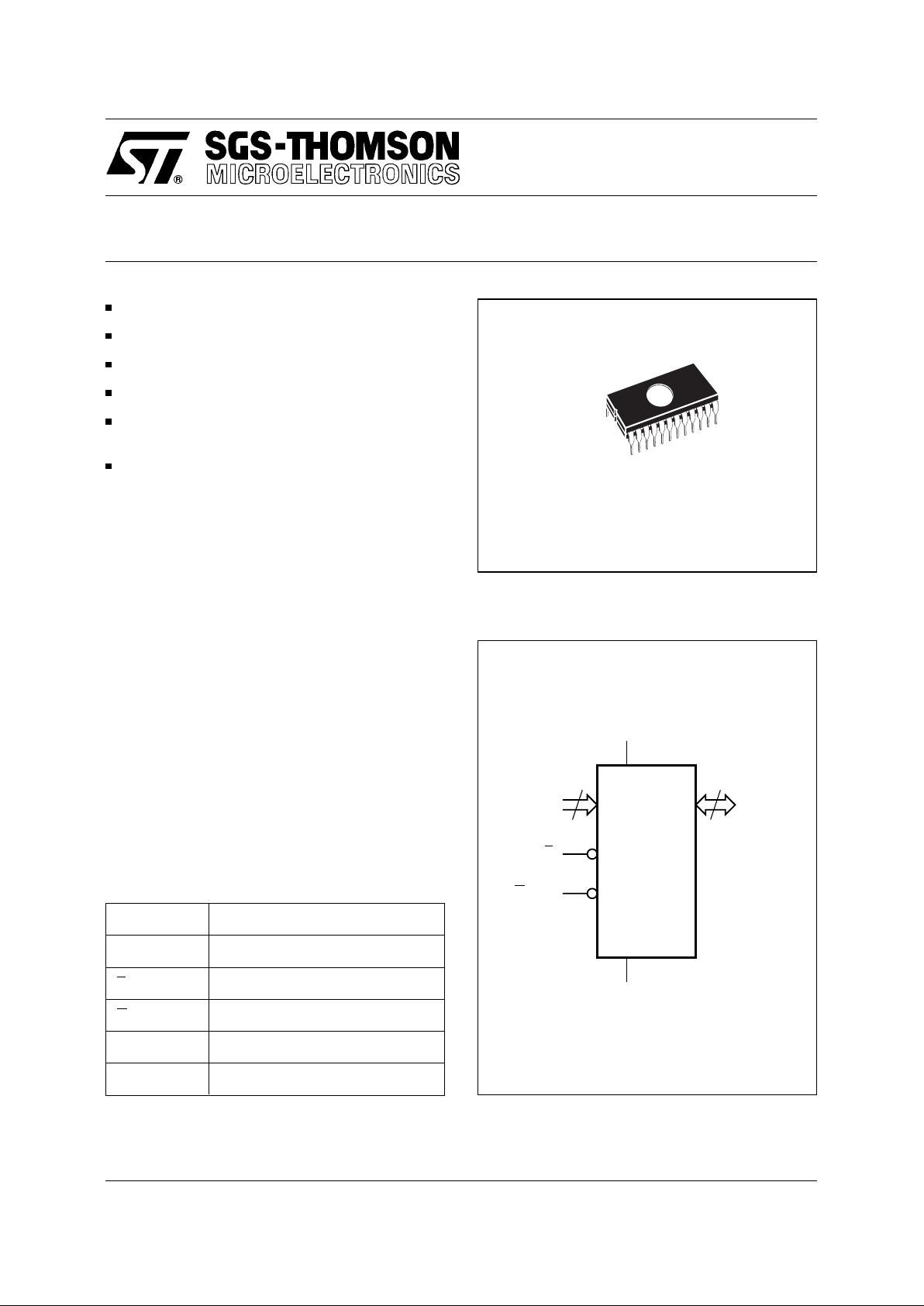
The M2732A is honsed in a 24 pin Window Ceramic
Frit-Seal Dual-in-Line pac kage. The transparent lid
allows the user to expose the chip t o ultraviolet light
to erase the bit patt ern. A new pattern can be then
written to the cleric e by following t he programmi ng
procedure.
A0 - A11 Address Inputs
Q0 - Q7 Data Outputs
E Chip Enable
GV
PP
Output Enable / Program Supply
V
CC
Supply Voltage
V
SS
Ground
T able 1. Signal Names
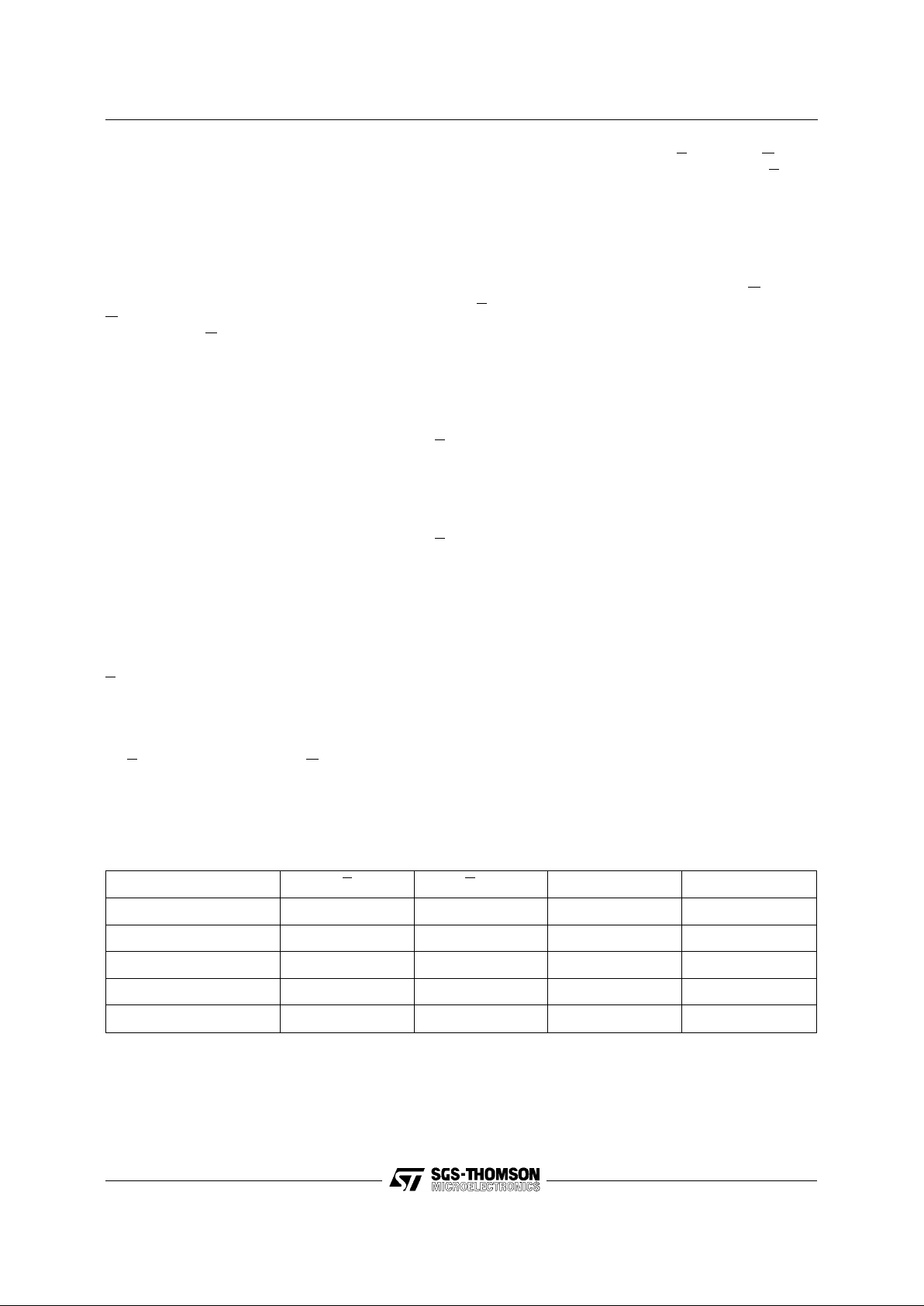
1
24
FDIP24W (F)
July 1994 1/9
Q2
V
SS
A3
A0
Q0
Q1
A2
A1
GV
PP
Q5
A10
E
Q3
A11
Q7
Q6
Q4
A4
V
CC
A7
AI00781
M2732A
8
1
2
3
4
5
6
7
9
10
11
12
20
19
18
17
16
15
A6
A5
A9
A8
23
22
21
14
13
24
Figure 2. DIP Pin Connecti ons
Symbol Parameter Value Unit
T
A
Ambient Operating Temperature grade 1
grade 6
0 to 70
–40 to 85
°C
T
BIAS
Temperature Under Bias grade 1
grade 6
–10 to 80
–50 to 95
°C
T
STG
Storage Temperature –65 to 125 °C
V
IO
Input or Output Voltages –0.6 to 6 V
V
CC
Supply Voltage –0.6 to 6 V
V
PP
Program Supply Voltage –0.6 to 22 V
Note: Except for the rating "Operating T emperature R ange", stresses above those lis ted in the Table "Absolute Maximum Ratings" may cause
permanent damage to the device. These are stress ratings only and opera tion of the device at these or any other conditions above those
indicated in the Operating sections of this specification is not implied. Exposure to Absolute Maximum Rati ng conditions for extended periods
may affect device reliabil ity. Refer also to the SGS-THOMSON SURE Program and other relevant quality documents.
Tab le 2. Absol ute Maxim u m Ratin gs
DEVICE OPER ATION
The six modes of operation for the M2732A are
listed in the Operating Modes Table. A single 5V
power supply is required in the read mode. All
inputs are TTL level except for V
PP.
Read Mode
The M2732A has two control functions, both of
which must be logically satisfied in order to obtai n
data at the outputs. Chip Enable (
E) is the power
control and should be used for device selection.
Output Enable (
G) is the output control and should
be used to gate data to the output pins, independent of device selection.
Assuming that the addresses are stable, address
access time (t
AVAQ
) is equal to the delay fr om E to
output (t
ELQV
). Data is available at the outputs after
the falling edge of
G, assuming that E has been low
and the addresses have been stable for at least
t
AVQ V-tGLQV
.
Stand by Mod e
The M2732A has a standby mode which reduces
the active power current by 70 %, from 125 mA to
35 mA. The M2732A is placed in the sta ndby mode
by applying a TTL high signal to
E input. When in
standby mode, the outputs are in a high impedance
state, independent of the
GVPP input.
Two Line Output Control
Because M2732A ’s are usually used in larger memory arrays, this product features a 2 line control
function which accommodates the use of multiple
memory connection. The two line control function
allows:
a. the lowest possible memory power dissipation,
b. complete assurance that output bus content i on
will not occur.
To most efficiently use these two control lines, it is
recommended that
E be decoded and used as the
primary device selecting function, while
G should
be made a common connection to all devices in the
array and connected to the
READ line from the
system control bus.
This ensures that all deselected memory devices
are in their low power standby mode and that the
output pins are only active when data is required
from a particular memory device.
2/9
M2732A
Programmin g
When delivered, and after each erasure, all bits of
the M2732A are in the “1" state. Data is introduce d
by selectively programming ”0’s" into the desired
bit locations. Although only “0’s” will be programmed, both “1’s” a nd “0’s” c an be present ed in
the data word. The only way to change a “0" to a
”1" is by ultraviolet light erasure.
The M2732A is in the programming mode when the
GVPP input is at 21V. A 0.1µF capacitor must be
placed across
GVPP and ground to suppress spurious voltage transients which may damage the
device. The data to be programmed is applied, 8
bits in parallel, to the data output pins. The levels
required for the address and data inputs are TTL.
When the address and data are stable, a 50ms,
active low, TTL program pulse is applied to the
E
input. A program pulse must be applied at each
address location to be programmed. Any location
can be programmed at any time - either individually ,
sequentially, or at random. T he program pulse has
a maximum width of 55ms. The M2732A must not
be programmed with a DC signal applied to the
E
input.
Programming of multiple M2732As in parallel with
the same data can be easily accomplished due to
the simplicity of the programming requirements.
Inputs of the paralleled M2732As may be connected together when they are programmed with
the same data. A low level TTL pulse applied to the
E input programs the paralleled 2732As.
Program Inhibit
Programming of multiple M2732As in parallel with
different data is also easily accomplished. Except
for
E, all like inputs (including GVPP) of the parallel
M2732As may be common. A T TL level program
pulse applied to a M2732A’s
E input with GV
PP
at
21V will program that M2732A. A high level
E input
inhibits the other M2732As from being programmed.
Program Verify
A verify should be performed on the programmed
bits to determine that they were correctly programmed. The verify is carried out with
GVPP and
E at VIL.
ERASURE OPERATION
The erasure characteristics of the M2732A are
such that erasure begins when the cells are exposed to light with wavelengths shorter than approximately 4000 Å. It should be noted that sunlight
and certain types of fluorescent lamps have wavelengths in the 3000-4000 Å range. Research shows
that constant exposure to room level fluorescent
lighting could erase a typical M2732A in approximately 3 years, while it would take approximately
1 week to cause erasure when exposed to the
direct sunlight. If the M2732A is to be exposed to
these types of lighting conditions for extended periods of time, it is suggested that opaque labels be
put over the M2732A window to prevent unintentional erasure.
The recommended erasure procedure for the
M2732A is exposure to shortwave ultraviolet light
which has a wavelength of 2537 Å. The integrated
dose (i.e. UV intensity x exposure time) for erasure
should be a minimum of 15 W-sec/cm
2
. The erasure time with this dosage is approximately 15 to
20 minutes using an ultraviolet lamp with 12000
µW/cm
2
power rating. The M2732A should be
placed within 2.5 cm of the lamp tubes during
erasure. Some lamps have a filter on their tubes
which should be removed before erasure.
Mode E GV
PP
V
CC
Q0 - Q7
Read V
IL
V
IL
V
CC
Data Out
Program VIL Pulse V
PP
V
CC
Data In
Verify V
IL
V
IL
V
CC
Data Out
Program Inhibit V
IH
V
PP
V
CC
Hi-Z
Standby V
IH
XVCCHi-Z
Note: X = VIH or VIL.
T ab le 3. Operating Modes
3/9
M2732A
 Loading...