

32-Mbit, dual I/O, 4-Kbyte subsector erase,
serial Flash memory with 75 MHz SPI bus interface
Features
■ SPI bus compatible serial interface
■ 75 MHz (maximum) clock frequency
■ 2.7 V to 3.6 V single supply voltage
■ Dual input/output instructions resulting in an
equivalent clock frequency of 150 MHz:
– Dual Output Fast Read instruction
– Dual Input Fast Program instruction
■ 32 Mbit Flash memory
– Uniform 4-Kbyte subsectors
– Uniform 64-Kbyte sectors
■ Additional 64-byte user-lockable, one-time
programmable (OTP) area
■ Erase capability
– Subsector (4-Kbyte) granularity
– Sector (64-Kbyte) granularity
– Bulk Erase (32 Mbit) in 17 s (typical with
V
= 9 V)
PP
■ Write protections
– Software write protection applicable to
every 64-Kbyte sector (volatile lock bit)
– Har dware write protection: protected area
size defined by three non- volatile bit s (BP0,
BP1 and BP2)
■ Deep Power-down mode: 5 µA (typical)
■ Electronic signature
– JEDEC standard two-byte signature
(7116h)
– Unique ID code (UID) +16 byte of CFI data
■ More than 100 000 write cycles per sector
■ More than 20 year data retention
■ Packages
– ECOPACK® (RoHS compliant)
M25PX32
VFQFPN8 (MP)
6 × 5 mm
SO8W (MW)
208 mils
SO16 (MF)
300 mils
September 2007 Rev 4 1/63
www.st.com
1

Contents M25PX32
Contents
1 Description . . . . . . . . . . . . . . . . . . . . . . . . . . . . . . . . . . . . . . . . . . . . . . . . . 6
2 Signal descriptions . . . . . . . . . . . . . . . . . . . . . . . . . . . . . . . . . . . . . . . . . . 9
2.1 Serial Data output (DQ1) . . . . . . . . . . . . . . . . . . . . . . . . . . . . . . . . . . . . . . 9
2.2 Serial Data input (DQ0) . . . . . . . . . . . . . . . . . . . . . . . . . . . . . . . . . . . . . . . 9
2.3 Serial Clock (C) . . . . . . . . . . . . . . . . . . . . . . . . . . . . . . . . . . . . . . . . . . . . . 9
2.4 Chip Select (S
2.5 Hold (HOLD
2.6 Write Protect/Enhanced Program supply voltage (W
2.7 V
2.8 V
supply voltage . . . . . . . . . . . . . . . . . . . . . . . . . . . . . . . . . . . . . . . . . . 10
CC
ground . . . . . . . . . . . . . . . . . . . . . . . . . . . . . . . . . . . . . . . . . . . . . . . . 10
SS
) . . . . . . . . . . . . . . . . . . . . . . . . . . . . . . . . . . . . . . . . . . . . . . 9
) . . . . . . . . . . . . . . . . . . . . . . . . . . . . . . . . . . . . . . . . . . . . . . . . 9
/VPP) . . . . . . . . . . . . 10
3 SPI modes . . . . . . . . . . . . . . . . . . . . . . . . . . . . . . . . . . . . . . . . . . . . . . . . 11
4 Operating features . . . . . . . . . . . . . . . . . . . . . . . . . . . . . . . . . . . . . . . . . 13
4.1 Page programming . . . . . . . . . . . . . . . . . . . . . . . . . . . . . . . . . . . . . . . . . . 13
4.2 Dual Input Fast Program . . . . . . . . . . . . . . . . . . . . . . . . . . . . . . . . . . . . . 13
4.3 Subsector Erase, Sector Erase and Bulk Erase . . . . . . . . . . . . . . . . . . . . 13
4.4 Polling during a Write, Program or Erase cycle . . . . . . . . . . . . . . . . . . . . 13
4.5 Fast Bulk Erase mode . . . . . . . . . . . . . . . . . . . . . . . . . . . . . . . . . . . . . . . 14
4.6 Active Power, Standby Power and Deep Power-down modes . . . . . . . . . 14
4.7 Status Register . . . . . . . . . . . . . . . . . . . . . . . . . . . . . . . . . . . . . . . . . . . . . 14
4.8 Protection modes . . . . . . . . . . . . . . . . . . . . . . . . . . . . . . . . . . . . . . . . . . . 15
4.8.1 Protocol-related protections . . . . . . . . . . . . . . . . . . . . . . . . . . . . . . . . . . 15
4.8.2 Specific hardware and software protection . . . . . . . . . . . . . . . . . . . . . . 16
4.9 Hold condition . . . . . . . . . . . . . . . . . . . . . . . . . . . . . . . . . . . . . . . . . . . . . . 18
5 Memory organization . . . . . . . . . . . . . . . . . . . . . . . . . . . . . . . . . . . . . . . 19
6 Instructions . . . . . . . . . . . . . . . . . . . . . . . . . . . . . . . . . . . . . . . . . . . . . . . 23
6.1 Write Enable (WREN) . . . . . . . . . . . . . . . . . . . . . . . . . . . . . . . . . . . . . . . 25
6.2 Write Disable (WRDI) . . . . . . . . . . . . . . . . . . . . . . . . . . . . . . . . . . . . . . . . 26
2/63

M25PX32 Contents
6.3 Read Identification (RDID) . . . . . . . . . . . . . . . . . . . . . . . . . . . . . . . . . . . . 27
6.4 Read Status Register (RDSR) . . . . . . . . . . . . . . . . . . . . . . . . . . . . . . . . . 28
6.4.1 WIP bit . . . . . . . . . . . . . . . . . . . . . . . . . . . . . . . . . . . . . . . . . . . . . . . . . . 28
6.4.2 WEL bit . . . . . . . . . . . . . . . . . . . . . . . . . . . . . . . . . . . . . . . . . . . . . . . . . 28
6.4.3 BP2, BP1, BP0 bits . . . . . . . . . . . . . . . . . . . . . . . . . . . . . . . . . . . . . . . . 28
6.4.4 TB bit . . . . . . . . . . . . . . . . . . . . . . . . . . . . . . . . . . . . . . . . . . . . . . . . . . . 29
6.4.5 SRWD bit . . . . . . . . . . . . . . . . . . . . . . . . . . . . . . . . . . . . . . . . . . . . . . . . 29
6.5 Write Status Register (WRSR) . . . . . . . . . . . . . . . . . . . . . . . . . . . . . . . . . 30
6.6 Read Data Bytes (READ) . . . . . . . . . . . . . . . . . . . . . . . . . . . . . . . . . . . . . 32
6.7 Read Data Bytes at higher speed (FAST_READ) . . . . . . . . . . . . . . . . . . 33
6.8 Dual Output Fast Read (DOFR) . . . . . . . . . . . . . . . . . . . . . . . . . . . . . . . . 34
6.9 Read Lock Register (RDLR) . . . . . . . . . . . . . . . . . . . . . . . . . . . . . . . . . . . 35
6.10 Read OTP (ROTP) . . . . . . . . . . . . . . . . . . . . . . . . . . . . . . . . . . . . . . . . . . 36
6.11 Page Program (PP) . . . . . . . . . . . . . . . . . . . . . . . . . . . . . . . . . . . . . . . . . 37
6.12 Dual Input Fast Program (DIFP) . . . . . . . . . . . . . . . . . . . . . . . . . . . . . . . . 39
6.13 Program OTP instruction (POTP) . . . . . . . . . . . . . . . . . . . . . . . . . . . . . . . 41
6.14 Write to Lock Register (WRLR) . . . . . . . . . . . . . . . . . . . . . . . . . . . . . . . . 43
6.15 Subsector Erase (SSE) . . . . . . . . . . . . . . . . . . . . . . . . . . . . . . . . . . . . . . 44
6.16 Sector Erase (SE) . . . . . . . . . . . . . . . . . . . . . . . . . . . . . . . . . . . . . . . . . . 45
6.17 Bulk Erase (BE) . . . . . . . . . . . . . . . . . . . . . . . . . . . . . . . . . . . . . . . . . . . . 46
6.18 Deep Power-down (DP) . . . . . . . . . . . . . . . . . . . . . . . . . . . . . . . . . . . . . . 47
6.19 Release from Deep Power-down (RDP) . . . . . . . . . . . . . . . . . . . . . . . . . . 48
7 Power-up and power-down . . . . . . . . . . . . . . . . . . . . . . . . . . . . . . . . . . . 49
8 Initial delivery state . . . . . . . . . . . . . . . . . . . . . . . . . . . . . . . . . . . . . . . . . 51
9 Maximum rating . . . . . . . . . . . . . . . . . . . . . . . . . . . . . . . . . . . . . . . . . . . . 51
10 DC and AC parameters . . . . . . . . . . . . . . . . . . . . . . . . . . . . . . . . . . . . . . 52
11 Package mechanical . . . . . . . . . . . . . . . . . . . . . . . . . . . . . . . . . . . . . . . . 58
12 Part numbering . . . . . . . . . . . . . . . . . . . . . . . . . . . . . . . . . . . . . . . . . . . . 61
13 Revision history . . . . . . . . . . . . . . . . . . . . . . . . . . . . . . . . . . . . . . . . . . . 62
3/63

List of tables M25PX32
List of tables
Table 1. Signal names . . . . . . . . . . . . . . . . . . . . . . . . . . . . . . . . . . . . . . . . . . . . . . . . . . . . . . . . . . . . 7
Table 2. Software protection truth table (Sectors 0 to 63, 64 Kbyte granularity) . . . . . . . . . . . . . . . 16
Table 3. Protected area sizes. . . . . . . . . . . . . . . . . . . . . . . . . . . . . . . . . . . . . . . . . . . . . . . . . . . . . . 17
Table 4. Memory organization . . . . . . . . . . . . . . . . . . . . . . . . . . . . . . . . . . . . . . . . . . . . . . . . . . . . . 20
Table 5. Instruction set . . . . . . . . . . . . . . . . . . . . . . . . . . . . . . . . . . . . . . . . . . . . . . . . . . . . . . . . . . . 24
Table 6. Read Identification (RDID) data-out sequence. . . . . . . . . . . . . . . . . . . . . . . . . . . . . . . . . . 27
Table 7. Status Register format . . . . . . . . . . . . . . . . . . . . . . . . . . . . . . . . . . . . . . . . . . . . . . . . . . . . 28
Table 8. Protection modes . . . . . . . . . . . . . . . . . . . . . . . . . . . . . . . . . . . . . . . . . . . . . . . . . . . . . . . . 31
Table 9. Lock Register out . . . . . . . . . . . . . . . . . . . . . . . . . . . . . . . . . . . . . . . . . . . . . . . . . . . . . . . . 35
Table 10. Lock Register in . . . . . . . . . . . . . . . . . . . . . . . . . . . . . . . . . . . . . . . . . . . . . . . . . . . . . . . . . 43
Table 11. Power-up timing and VWI threshold . . . . . . . . . . . . . . . . . . . . . . . . . . . . . . . . . . . . . . . . . . 50
Table 12. Absolute maximum ratings . . . . . . . . . . . . . . . . . . . . . . . . . . . . . . . . . . . . . . . . . . . . . . . . . 51
Table 13. Operating conditions. . . . . . . . . . . . . . . . . . . . . . . . . . . . . . . . . . . . . . . . . . . . . . . . . . . . . . 52
Table 14. AC measurement conditions. . . . . . . . . . . . . . . . . . . . . . . . . . . . . . . . . . . . . . . . . . . . . . . . 5 2
Table 15. Capacitance . . . . . . . . . . . . . . . . . . . . . . . . . . . . . . . . . . . . . . . . . . . . . . . . . . . . . . . . . . . . 52
Table 16. DC characteristics. . . . . . . . . . . . . . . . . . . . . . . . . . . . . . . . . . . . . . . . . . . . . . . . . . . . . . . . 53
Table 17. AC characteristics. . . . . . . . . . . . . . . . . . . . . . . . . . . . . . . . . . . . . . . . . . . . . . . . . . . . . . . . 54
Table 18. VFQFPN8 (MLP8) 8-lead very thin fine pitch quad flat package no lead,
6 × 5 mm, package mechanical data . . . . . . . . . . . . . . . . . . . . . . . . . . . . . . . . . . . . . . . . . 58
Table 19. SO8W 8-lead plastic small outline, 208 mils body width, package
mechanical data. . . . . . . . . . . . . . . . . . . . . . . . . . . . . . . . . . . . . . . . . . . . . . . . . . . . . . . . . 5 9
Table 20. SO16 wide - 16-lead plastic small outline, 300 mils body width, mechanical data. . . . . . . 60
Table 21. Ordering information scheme . . . . . . . . . . . . . . . . . . . . . . . . . . . . . . . . . . . . . . . . . . . . . . . 61
Table 22. Document revision history . . . . . . . . . . . . . . . . . . . . . . . . . . . . . . . . . . . . . . . . . . . . . . . . . 62
4/63

M25PX32 List of figures
List of figures
Figure 1. Logic diagram . . . . . . . . . . . . . . . . . . . . . . . . . . . . . . . . . . . . . . . . . . . . . . . . . . . . . . . . . . . . 7
Figure 2. VFQFPN and SO8 connections . . . . . . . . . . . . . . . . . . . . . . . . . . . . . . . . . . . . . . . . . . . . . . 7
Figure 3. SO16 connections . . . . . . . . . . . . . . . . . . . . . . . . . . . . . . . . . . . . . . . . . . . . . . . . . . . . . . . . 8
Figure 4. Bus Master and memory devices on the SPI bus. . . . . . . . . . . . . . . . . . . . . . . . . . . . . . . . 11
Figure 5. SPI modes supported . . . . . . . . . . . . . . . . . . . . . . . . . . . . . . . . . . . . . . . . . . . . . . . . . . . . . 12
Figure 6. Hold condition activation. . . . . . . . . . . . . . . . . . . . . . . . . . . . . . . . . . . . . . . . . . . . . . . . . . . 18
Figure 7. Block diagram. . . . . . . . . . . . . . . . . . . . . . . . . . . . . . . . . . . . . . . . . . . . . . . . . . . . . . . . . . . 19
Figure 8. Write Enable (WREN) instruction sequence. . . . . . . . . . . . . . . . . . . . . . . . . . . . . . . . . . . . 25
Figure 9. Write Disable (WRDI) instruction sequence . . . . . . . . . . . . . . . . . . . . . . . . . . . . . . . . . . . . 26
Figure 10. Read Identification (RDID) instruction sequence and data-out sequence . . . . . . . . . . . . . 27
Figure 11. Read Status Register (RDSR) instruction sequence and data-out sequence . . . . . . . . . . 29
Figure 12. Write Status Register (WRSR) instruction sequence . . . . . . . . . . . . . . . . . . . . . . . . . . . . . 30
Figure 13. Read Data Bytes (READ) instruction sequence and data-out sequence . . . . . . . . . . . . . . 32
Figure 14. Read Data Bytes at higher speed (FAST_READ) instruction sequence
and data-out sequence . . . . . . . . . . . . . . . . . . . . . . . . . . . . . . . . . . . . . . . . . . . . . . . . . . . . 33
Figure 15. Dual Output Fast Read instruction sequence . . . . . . . . . . . . . . . . . . . . . . . . . . . . . . . . . . . 34
Figure 16. Read Lock Register (RDLR) instruction sequence and data-out sequence . . . . . . . . . . . . 35
Figure 17. Read OTP (ROTP) instruction and data-out sequence . . . . . . . . . . . . . . . . . . . . . . . . . . . 36
Figure 18. Page Program (PP) instruction sequence . . . . . . . . . . . . . . . . . . . . . . . . . . . . . . . . . . . . . 38
Figure 19. Dual Input Fast Program (DIFP) instruction sequence . . . . . . . . . . . . . . . . . . . . . . . . . . . . 40
Figure 20. Program OTP (POTP) instruction sequence . . . . . . . . . . . . . . . . . . . . . . . . . . . . . . . . . . . 42
Figure 21. How to permanently lock the 64 OTP bytes . . . . . . . . . . . . . . . . . . . . . . . . . . . . . . . . . . . . 42
Figure 22. Write to Lock Register (WRLR) instruction sequence. . . . . . . . . . . . . . . . . . . . . . . . . . . . . 43
Figure 23. Subsector Erase (SSE) instruction sequence. . . . . . . . . . . . . . . . . . . . . . . . . . . . . . . . . . . 44
Figure 24. Sector Erase (SE) instruction sequence. . . . . . . . . . . . . . . . . . . . . . . . . . . . . . . . . . . . . . . 45
Figure 25. Bulk Erase (BE) instruction sequence . . . . . . . . . . . . . . . . . . . . . . . . . . . . . . . . . . . . . . . . 46
Figure 26. Deep Power-down (DP) instruction sequence . . . . . . . . . . . . . . . . . . . . . . . . . . . . . . . . . . 47
Figure 27. Release from Deep Power-down (RDP) instruction sequence. . . . . . . . . . . . . . . . . . . . . . 48
Figure 28. Power-up timing . . . . . . . . . . . . . . . . . . . . . . . . . . . . . . . . . . . . . . . . . . . . . . . . . . . . . . . . . 50
Figure 29. AC measurement I/O waveform . . . . . . . . . . . . . . . . . . . . . . . . . . . . . . . . . . . . . . . . . . . . . 52
Figure 30. Serial input timing . . . . . . . . . . . . . . . . . . . . . . . . . . . . . . . . . . . . . . . . . . . . . . . . . . . . . . . . 55
Figure 31. Write Protect Setup and Hold timing during WRSR when SRWD=1 . . . . . . . . . . . . . . . . . 56
Figure 32. Hold timing . . . . . . . . . . . . . . . . . . . . . . . . . . . . . . . . . . . . . . . . . . . . . . . . . . . . . . . . . . . . . 56
Figure 33. Output timing . . . . . . . . . . . . . . . . . . . . . . . . . . . . . . . . . . . . . . . . . . . . . . . . . . . . . . . . . . . 57
Figure 34. V
Figure 35. VFQFPN8 (MLP8) 8-lead very thin fine pitch quad flat package no lead,
Figure 36. SO8W 8-lead plastic small outline, 208 mils body width, package outline. . . . . . . . . . . . . 59
Figure 37. SO16 wide - 16-lead plastic small outline, 300 mils body width, package outline . . . . . . . 60
timing. . . . . . . . . . . . . . . . . . . . . . . . . . . . . . . . . . . . . . . . . . . . . . . . . . . . . . . . . . . . . 57
PPH
6 × 5 mm, package outline . . . . . . . . . . . . . . . . . . . . . . . . . . . . . . . . . . . . . . . . . . . . . . . . . 58
5/63

Description M25PX32
1 Description
The M25PX32 is a 32 Mbit (4 Mb x 8) serial Flash memory, with advanced write protection
mechanisms, accessed by a high speed SPI-compatible bus.
The M25PX32 supports two new, high-performance dual input/output instructions:
● Dual Output Fast Read (DOFR) instruction used to read data a t up t o 75 MHz by using
both pin DQ1 and pin DQ0 as outputs
● Dual Input Fast Program (DIFP) instruction used to program data at up to 75 MHz by
using both pin DQ1 and pin DQ0 as inputs
These new instructions double the transfer bandwidth for read and program operations.
The memory can be programmed 1 to 256 bytes at a time, using the Page Program
instruction.
The memory is organized as 64 sectors that are further divided into 16 subsectors each
(1024 subsectors in total).
The memory can be erased a 4-Kbyte subsector at a time, a 64-Kbyte sect or at a time , or as
a whole. It can be Write Protected by software using a mix of volatile and non-volatile
protection features, depending on the application needs. The protection granularity is of 64
Kbytes (sector granularity).
An enhanced Fast Bulk Erase mode is available to speed up Bulk Erase operations in
factory environment. The device enters this mode whenever the V
the Write Protect/Enhanced Program supply voltage pin (W
/VPP).
voltage is applied to
PPH
The M25PX32 has 64 One-Time-Programmable bytes (OTP bytes) that can be read and
programmed using two dedicated instructions, Read OTP (ROTP) and Program OTP
(POTP), respectively. These 64 bytes can be permanently locked by a particular Program
OTP (POTP) sequence. Once they have been lock ed, they become read-only and this state
cannot be reverted.
Further features are available as additional security options. More information on these
security features is available, upon completion of an NDA (nondisclosure agreement), and
are, therefore, not described in this datasheet. For more details of this option contact your
nearest ST Sales office.
In order to meet environmental requirements, ST offers the M25PX32 in ECOPACK®
packages. ECOPACK® packages are Lead-free and RoHS compliant.
ECOPACK® is an ST trademark. ECOPACK® specifications are available at: www.st.com.
6/63
M25PX32 Description
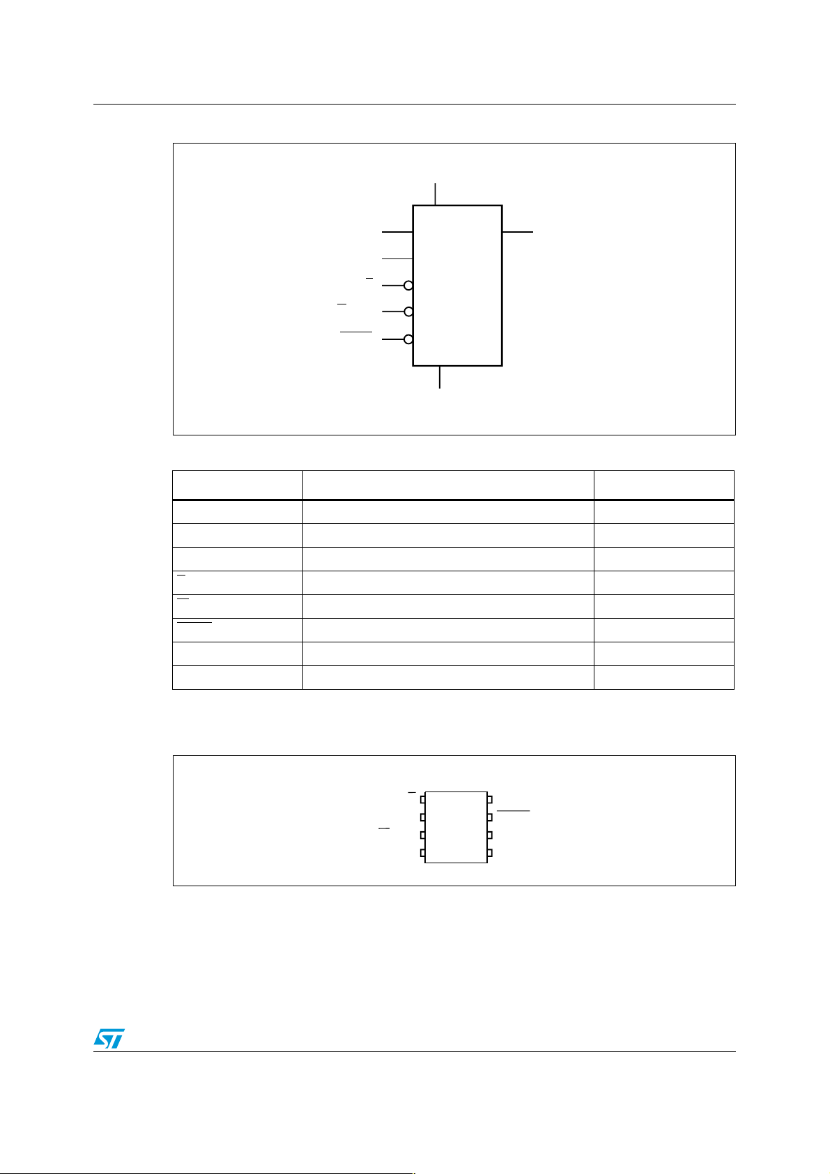
Figure 1. Logic diagram
V
CC
DQ0
DQ1
C
M25PX32
W/V
S
PP
HOLD
V
Table 1. Signal names
SS
AI14228
Signal name Function Direction
C Serial Clock Input
DQ0 Serial Data input I/O
DQ1 Serial Data output I/O
(1)
(2)
S Chip Select Input
/V
W
PP
HOLD
Write Protect/Enhanced Program supply voltage Input
Hold Input
V
CC
V
SS
1. Serves as an output during Dual Output Fast Read (DOFR) instructions.
2. Serves as an input during Dual Input Fast Program (DIFP) instructions.
Supply voltage
Ground
Figure 2. VFQFPN and SO8 connections
M25PX32
SV
1
2
W/V
1. There is an exposed central pad on the underside of the VFQFPN package. This is pulled, internally, to
V
, and must not be allowed to be connected to any other voltage or signal line on the PCB.
SS
2. See Package mechanical section for package dimensions, and how to identify pin-1.
PP
SS
3
4
7/63
8
CC
7
HOLDDQ1
6
C
5
DQ0V
AI13720b

Description M25PX32
Figure 3. SO16 connections
M25PX32
HOLD
V
CC
DU
DU
DU
S
DQ1
1. DU = Don’t use.
2. See Package mechanical section for package dimensions, and how to identify pin-1.
16
1
2
3
4
5
6
7
8
15
14
13
12
11
10
C
DQ0
DUDU
DU
DU
DU
V
SS
9
W/V
PP
AI13721b
8/63

M25PX32 Signal descriptions
2 Signal descriptions
2.1 Serial Data output (DQ1)
This output signal is used to transf er data serially out of the device. Data are shifted out on
the falling edge of Serial Clock (C).
During the Dual Input Fast Program (DIFP) instruction, pin DQ1 is used as an input. It is
latched on the rising edge of the Serial Clock (C).
2.2 Serial Data input (DQ0)
This input signal is used to transfer data serially into the device. It receives instructions,
addresses, and the data to be programmed. Values are latched on the rising edge of Serial
Clock (C).
During the Dual Output Fast Read (DOFR) instruction, pin DQ0 is used as an output. Data
are shifted out on the falling edge of the Serial Clock (C).
2.3 Serial Clock (C)
This input signal provides the timing of the serial interface. Instructions, addresses, or data
present at Serial Data input (DQ0) are latched on the rising edge of Serial Clock (C). Data
on Serial Data output (DQ1) changes after the falling edge of Serial Clock (C).
2.4 Chip Select (S)
When this input signal is High, the device is deselec ted and Serial Data output (DQ1) is at
high impedance. Unless an internal Program, Erase or Write Status Register cycle is in
progress, the device will be in the Standby Power mode (this is not the Deep Power-down
mode). Driving Chip Select (S
After Power-up, a falling edge on Chip Select (S
instruction.
2.5 Hold (HOLD)
The Hold (HOLD) signal is used to pause any serial communications with the de vice without
deselecting the device.
During the Hold condition, the Serial Data output (DQ1) is hi gh impe dance, and Serial Data
input (DQ0) and Serial Clock (C) are Don’t care.
To start the Hold condition, the device must be selected, with Chip Select (S
) Low enables the device, placing it in the Active Power mode .
) is required prior to the start of any
) driven Low.
9/63

Signal descriptions M25PX32
2.6 Write Protect/Enhanced Program supply voltage (W/VPP)
W/VPP is both a control input and a power supply p in. The two functions ar e selected by the
voltage range app lied to the pin.
If the W
input. This input signal is used to freeze the size of the area of memory that is protected
against program or erase instructions (as specified by the values in the BP2, BP1 and BP0
bits of the Status Register. See Table 9).
If V
during the Bulk Erase cycle. In this case V
completed.
/V
input is kept in a low voltage range (0 V to VCC) the pin is seen as a control
PP
is in the range of V
PP
PPH
2.7 VCC supply voltage
VCC is the supply voltage.
2.8 VSS ground
VSS is the reference for the VCC supply voltage.
(as defined in Table 14) it acts as an additional power supply
must be stable until the Bulk Er ase algorithm is
PP
10/63
M25PX32 SPI modes
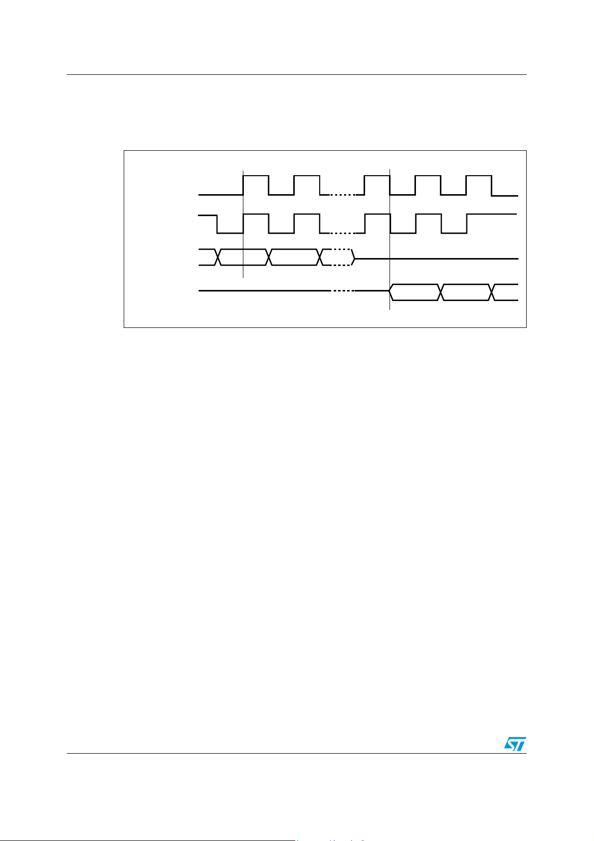
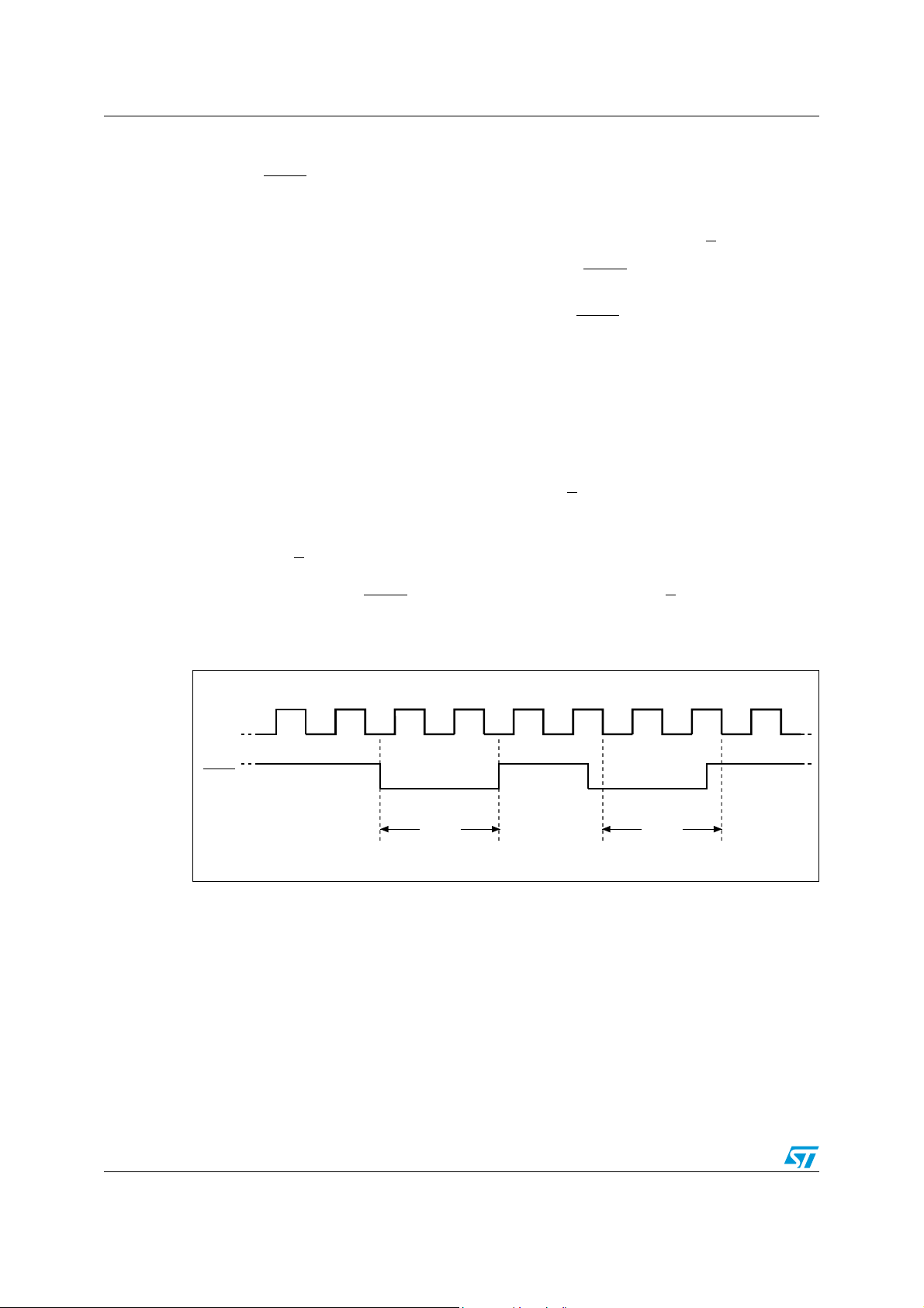
3 SPI modes
These devices can be drive n by a microcontroller with its SPI peripheral running in either of
the two following modes:
● CPOL=0, CPHA=0
● CPOL=1, CPHA=1
For these two modes, input data is latched in on the rising edge of Serial Clock (C), and
output data is available from the falling edge of Serial Clock (C).
The difference between the two modes, as sho wn in Figure 5, is the clock polarity when the
bus master is in Standby mode and not transferring data:
● C remains at 0 for (CPOL=0, CPHA=0)
● C remains at 1 for (CPOL=1, CPHA=1)
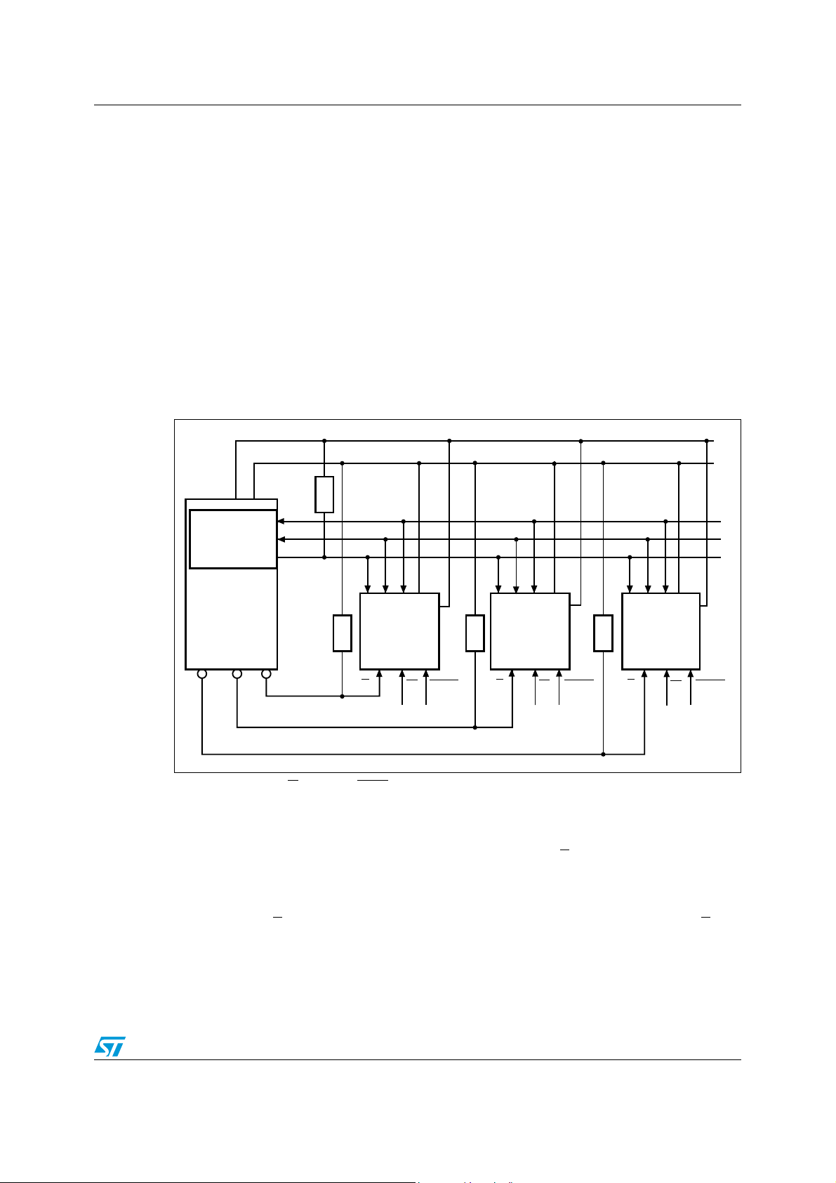
Figure 4. Bus Master and memory devices on the SPI bus
V
SS
V
CC
R
SPI interface with
(CPOL, CPHA) =
(0, 0) or (1, 1)
SPI Bus Master
CS3 CS2 CS1
1. The Write Protect (W) and Hold (HOLD) signals should be driven, High or Low as appropriate.
SDO
SDI
SCK
device
V
CC
HOLD
W
C
V
SS
DQ1 DQ0
SPI memory
S
C
DQ1DQ0
RRR
SPI memory
S
device
V
CC
W
HOLD
C
V
SS
S
DQ1DQ0
SPI memory
device
W
V
CC
V
SS
HOLD
AI13725b
Figure 4 shows an exampl e of three de vices connected to an MCU, on an SPI bus. Only one
device is selected at a time, so only one device drives t he Serial Data ou tput ( DQ1) line a t a
time, the other devices are high impedance. Resistors R (represented in Figure 4) ensure
that the M25PX32 is not selected if the Bus Master leaves the S
line in the high impedance
state. As the Bus Master may enter a state where all inputs/outputs are in high impedance
at the same time (for example, when the Bus Master is reset), the clock line (C) must be
connected to an external pull-down resistor so that, when all inputs/outputs become high
impedance, the S
C do not become High at the same time, and so, that the t
typical value of R is 100 kΩ, assuming that the time constant R*C
line is pulled High while the C line is pulled Low (thus ensuring that S a nd
requirement is met). The
SHCH
(Cp = parasitic
p
capacitance of the bus line) is shorter than the time during which the Bus Master leaves the
SPI bus in high impedance.
11/63
SPI modes M25PX32
Example: Cp = 50 pF, that is R*Cp = 5 µs <=> the application must ensure that the Bus
Master never leaves the SPI bus in the hig h impedance state for a time period shorter than
5µs.
Figure 5. SPI modes supported
CPHA
CPOL
C
0
0
1
1
C
DQ0
DQ1
MSB
MSB
AI13730
12/63

M25PX32 Operating features
4 Operating features
4.1 Page programming
To program one data byte, two instructions are required: Write Enab le (WREN), which is one
byte, and a Page Program (PP) sequence, which consists of four bytes plus data. This is
followed by the internal Program cycle (of duration t
To spread this overhead, the P age Program (PP) instruction allows up to 256 bytes to be
programmed at a time (changing bits from 1 to 0), provided that they lie in consecutive
addresses on the same page of memory.
For optimized timings, it is recommended to use the Page Program (PP) instruction to
program all consecutive targeted bytes in a single sequence versus using several Page
Program (PP) sequences with each containing only a few bytes (see Page Program (PP)
and Table 17: AC characteristics).
4.2 Dual Input Fast Program
The Dual Input Fast Program (DIFP) instruction makes it possible to program up to 256
bytes using two input pins at the same time (by changing bits from 1 to 0).
PP
).
For optimized timings, it is recommended to use the Dual Input Fast Program (DIFP)
instruction to program all consecutive targeted bytes in a single sequence rather to using
several Dual Input Fast Program (DIFP) sequences each containing only a few bytes (see
Section 6.12: Dual Input Fast Program (DIFP)).
4.3 Subsector Erase, Sector Erase and Bulk Erase
The Page Program (PP) instruction allows bits to be reset from 1 to 0. Before this can be
applied, the bytes of memory need to have been erased to all 1s (FFh). This can be
achieved either a subsector at a time, using the Subsector Erase (SSE) instruction, a sector
at a time, using the Sector Erase (SE) instruction, or throughout the entire memory, using
the Bulk Erase (BE) instruction. This starts an internal Erase cycle (of duration t
t
).
BE
The Erase instruction must be preceded by a Write Enable (WREN) instruction.
4.4 Polling during a Write, Program or Erase cycle
A further improvement in the time to Write Status Register (WRSR), Program OTP (POTP),
Program (PP), Dual Input F ast Program (DIFP) or Erase (SSE, SE or BE) can be achieved
by not waiting for the worst case delay (t
(WIP) bit is provided in the Status Register so that the application program can monitor its
value, polling it to establish when the previous Write cycle, Program cycle or Erase cycle is
complete.
, tPP, t
W
, tSE, or tBE). The Write In Progress
SSE
SSE
, tSE or
13/63

Operating features M25PX32
4.5 Fast Bulk Erase mode
The Fast Bulk Erase mode is used to speed up Bulk Erase operations. The device enters
the Fast Bulk Er ase mode d uring a Bulk Erase inst ruction whene v er a voltage equal to V
is applied to the W
/VPP pin.
PPH
The use of the Fast Bu lk Erase mode requires specific operating conditions in a ddition to the
normal ones (V
● the voltage applied to the W/V
● ambient temperature, T
● the cumulated time during which W/V
must be within the normal operating range):
CC
pin must be equal to V
PP
must be 25 °C ±10 °C,
A
is at V
PP
PPH
(see Table 13)
PPH
should be less than 80 hours.
4.6 Active Po wer, Standby Power and Deep Power-down modes
When Chip Select (S) is Low, the device is selected, and in the Active Power mode.
When Chip Select (S
) is High, the device is deselect ed, but coul d remain in the Activ e P o wer
mode until all internal cycles have completed (Program, Erase, Write Status Register). The
device then goes in to the Standby Power mode. The device consumption drops to I
The Deep Power-down mode is entered when the specific instruction (the Deep Powerdown (DP) instruction) is executed. The device consumption drops further to I
device remains in this mode until another specific instruction (the Release from Deep
Power-down (RDP) instruction) is executed.
While in the Deep Power-down mode, the device ignores all Write, Program and Erase
instructions (see Deep Power-down (DP)), this can be used as an extra software protection
mechanism, when the device is not in active use, to protect the device from inadvertent
Write, Program or Erase instructions.
4.7 Status Register
The Status Register contains a number of status a nd cont rol bits that can b e read or set (as
appropriate) by specific instructions. See Section 6.4: Read Status Register (RDSR) for a
detailed description of the Status Register bits.
CC2
CC1
. The
.
14/63

M25PX32 Operating features
4.8 Protection modes
There are protocol-related and specific hardware and software protection modes. They are
described below.
4.8.1 Protocol-related protections
The environments where non-volatile memory devices are used can be very noisy. No SPI
device can operate correctly in the presence of excessive noise. To help combat this, the
M25PX32 features the following data protection mechanisms:
● P ower On Reset and an internal timer (t
changes while the power supply is outside the operating specification
● Program, Er ase and Write Status Register inst ructions are chec k ed tha t the y co nsist of
a number of clock pulses tha t is a multiple of eight, before they are accepted for
execution
● All instructions that modify data must be prec eded by a Write Enable (WREN)
instruction to set the Write Enable Latch (WEL) bit . This bit is re turned to its re set state
by the following events:
–Power-up
– Write Disable (WRDI) instruction completion
– Write Status Register (WRSR) instruction completion
– Write to Lock Register (WRLR) instruction completion
– Program OTP (POTP) instruction completion
– Page Program (PP) instruction completion
– Dual Input Fast Program (DIFP) instruction completion
– Subsector Erase (SSE) instruction completion
– Sector Erase (SE) instruction completion
– Bulk Erase (BE) instruction completion
● In addition to the lo w power consumption feature , the Deep Power-down mode offers
extra softw are protection, as all Write, Program and Erase instructions are ignored.
) can provide protection against inadvertent
PUW
15/63
Operating features M25PX32
4.8.2 Specific hardware and software protection
There are two software protected modes , SPM1 and SPM2, that can b e combined to protect
the memory array as required. Th e SPM 2 can be lo cked by hardw are wit h th e help o f th e W
input pin.
SPM1 and SPM2
● The first software protected mode (SPM1) is managed by specific Lock Registers
assigned to each 64 Kbyte sector.
The Lock Registers can be read and written using the Read Loc k Register (RDLR) a nd
Write to Lock Register (WRLR) instructions.
In each Lock Register two bits control the protection of each sector: the Write Lock bit
and the Lock Down bit.
– Write Lock bit:
The Write Lock bit determines whether the contents of the sector can be modifi ed
(using the Write, Program or Erase instructions). When the Write Loc k b it is set to
‘1’, the sector is write protected – any operations t hat attempt to change the data
in the sector will fail. When the Write Lock bit is reset to ‘0’, the sector is not write
protected by the Lock Register, and may be modified.
– Lock Down bit:
The Lock Down bit pro vides a mechanism for protecting software da ta from simple
hacking and malicious attack. When the Lock Down bit is set, ‘1’, further
modification to the Write Lock and Lock Down bits cannot be performed. A powerup, is required before changes to these bits can be made. When the Lock Down bit
is reset, ‘0’, the Write Lock and Lock Down bits can be changed.
The definition of the Lock Register bits is given in Table 9: Lock Register out.
Table 2. Software protection truth table ( Sectors 0 to 63, 64 Kbyte granularity)
Sector Lock
Register
Protection status
Lock
Down bit
00
01
10
11
● the second software protected mode (SPM2) uses the Block Protect bits (see
Write
Lock bit
Sector unprotected from Program/Erase/Write operations, protection status
reversible
Sector protected from Program/Erase/Write operations, protection status
reversible
Sector unprotected from Program/Erase/Write operations,
Sector protection status cannot be changed except by a Power-up.
Sector protected from Program/Erase/Write operations,
Sector protection status cannot be changed except by a Power-up.
Section 6.4.3: BP2, BP1, BP0 bits) and the Top/Bottom bit (see Section 6.4.4: TB bit) to
allow part of the memory to be configured as read-only.
16/63
M25PX32 Operating features
Table 3. Protected area sizes
Status Register
contents
TB
BP
BP
bit
bit 2
bit 1
BP
bit 0
Protected area Unprotected area
0 0 0 0 none All sectors
Memory content
(1)
(64 sectors: 0 to 63)
0 0 0 1 Upper 64th (Sector 63) Lower 63/64ths (63 sectors: 0 to 62)
0 0 1 0 Upper 32nd (two sectors: 62 and 63) Lower 31/32nds (62 sectors: 0 to 61)
0 0 1 1
0 1 0 0 Upper eighth (eight sectors: 56 to 63)
0 1 0 1
0 1 1 0
Upper sixteenth (four sectors: 60 to
63)
Upper quarter (sixteen sectors: 48 to
63)
Upper half (thirty-two sectors: 32 to
63)
Lower 15/16ths (60 sectors: 0 to 59)
Lower seven-eighths (56 sectors: 0
to 55)
Lower three-quarters (48 sectors: 0
to 47)
Lower half (32 sectors: 0 to 31)
0 1 1 1 All sectors (64 sectors: 0 to 63) none
(1)
1 0 0 0 none All sectors
(64 sectors: 0 to 63)
1 0 0 1 Lower 64th (sector 0) Upper 63/64ths (63 sectors: 1 to 63)
1 0 1 0 Lower 32nd (two sectors: 0 and 1) Upper 31/32ths (62 sectors: 2 to 63)
1 0 1 1 Lower 16th (four sectors: 0 to 3) Upper 15/16ths (60 sectors: 4 to 63)
1 1 0 0 Lower 8th (eight sectors: 0 to 7) Upper 7/8ths (56 sectors: 8 to 63)
1 1 0 1 Lower 4th (sixteen sectors: 0 to 15) Upper 3/4ths (48 sectors: 16 to 63)
1110
Lower half (thirty-two sectors: 0 to
31)
Upper half (32 sectors: 32 to 63)
1 1 1 1 All sectors (64 sectors: 0 to 63) none
1. The device is ready to accept a Bulk Erase instruction if, and only if, all Block Protect (BP2, B P1, BP0) are
0.
As a second level of protection, the Write Protect signal (applied on the W/VPP pin) can
freeze the Status Register in a read-only mode. In this mode, the Block Protect bits (BP2,
BP1, BP0) and the Status Register Write Disable bit (SRWD) are protected. For more
details, see Section 6.5: Write Status Register (WRSR).
17/63
Operating features M25PX32
4.9 Hold condition
The Hold (HOLD) signal is used to pause any serial communications with the de vice without
resetting the clocking sequence. However, taking this signal Low does not terminate any
Write Status Register, Pro gram or Erase cycle that is currently in progress.
To enter the Hold condition, the device must be selected, with Chip Select (S
The Hold condition starts on the falling edge of the Hold (HOLD
) signal, provided that this
) Low.
coincides with Serial Clock (C) being Low (as shown in Figure 6).
The Hold condition ends on the rising edge of the Hold (HOLD
) signal, provided that this
coincides with Serial Clock (C) being Low.
If the falling edge does not coincide with Serial Clock (C) being Low, the Hold condition
starts after Serial Clock (C) next goes Low. Similarly, if the rising edge does not coincide
with Serial Clock (C) being Low, the Hold condition ends after Serial Clock (C) next goes
Low. (This is shown in Figure 6).
During the Hold condition, the Serial Data output (DQ1) is hi gh impe dance, and Serial Data
input (DQ0) and Serial Clock (C) are Don’t care.
Normally , the de vice is k ept selected, with Chip Select (S
) driven Low, for the whole dur ation
of the Hold condition. This is to ensure that the state of the internal logic remains unchanged
from the moment of entering the Hold condition.
If Chip Select (S
) goes High while the device is in the Hold condition, t his has the effect of
resetting the internal logic of the device. To restart communication with the device, it is
necessary to drive Hold (HOLD
) High, and then to drive Chip Select (S) Low. This prevents
the device from going back to the Hold condition.
Figure 6. Hold condition activation
C
HOLD
Hold
Condition
(standard use)
18/63
Hold
Condition
(non-standard use)
AI02029D
M25PX32 Memory organization
5 Memory organization
The memory is organized as:
● 4 194 304 bytes (8 bits each)
● 1024 subsectors (4 Kbytes each)
● 64 sectors (64 Kbytes each)
● 16384 pages (256 bytes each)
● 64 OTP bytes located outside the main memory array
Each page can be individually prog rammed ( bits are prog rammed from 1 t o 0). The de vice is
Subsector, Sector or Bulk Erasable (bits are erased from 0 to 1) but not Page Erasable.
Figure 7. Block diagram
HOLD
V
DQ0
DQ1
PP
Control Logic
S
C
Address Register
and Counter
Y Decoder
High Voltage
Generator
I/O Shift Register
256 Byte
Data Buffer
64 OTP bytes
Status
Register
3FFFFFh
Configurable OTP
area in main
memory array
00000h
256 Bytes (Page Size)
X Decoder
000FFh
AI13722
19/63
 Loading...