

1/34December 2002
M25P20
2 Mbit, Low Voltage, Serial Flash Memory
With 25 MHz SPI Bus Interface
FEATURES SUMMARY
■ 2 Mbit of Flash Memory
■ Page Program (up to 256 Bytes) in 1.5ms
(typical)
■ Sector Erase (512 Kbit) in 2 s (typical)
■ Bulk Eras e (2 Mbit) in 3 s ( typ ic al)
■ 2.7 V to 3.6 V Single Supply Voltage
■ SPI Bus Compatible Serial Interface
■ 25 MHz Clock Rate (maximum)
■ Deep Power-down Mode 1 µA (typical)
■ Electronic Signature (11h)
■ More than 100,000 Erase/Program Cycles per
Sector
■ More than 20 Year Data Retention
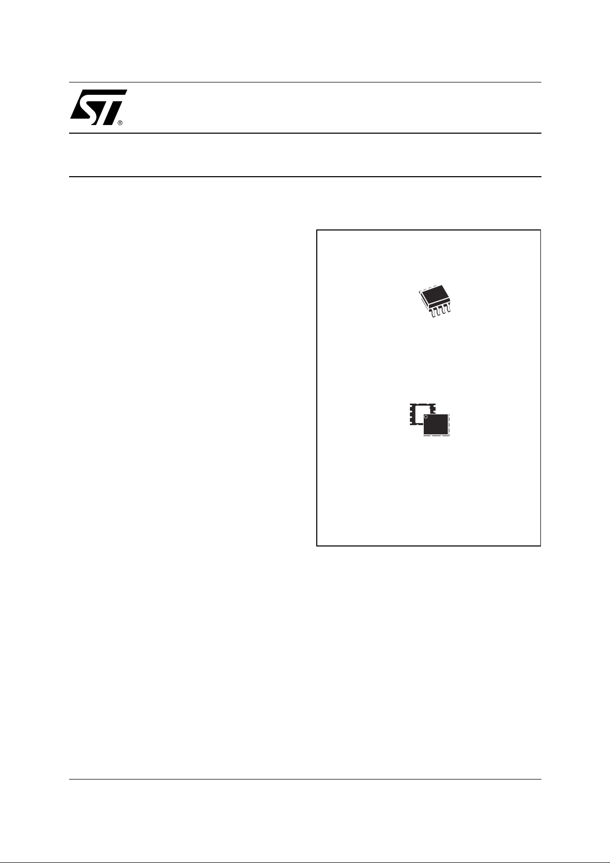
Figure 1. Packages
SO8 (MN)
150 mil width
8
1
VFQFPN8 (MP)
(MLP8)
M25P20
2/34
SUMMARY DESCRIPTION
The M25P 20 is a 2 Mbit ( 256K x 8) Serial Flash
Memory, with advanced write protection mechanisms, accessed by a high speed SPI -compatible
bus.
The memory can be programmed 1 to 256 bytes at
a time, using the Page Program instruction.
The memory is organized as 4 s ectors, eac h containing 256 pages. E ach page is 25 6 bytes wide.
Thus, the whole memory can be viewed as consisting of 1024 pages, or 262,144 bytes.
The whole memory can be eras ed using the B ulk
Erase instruction, or a sector at a time, us ing the
Sector Erase instruction.
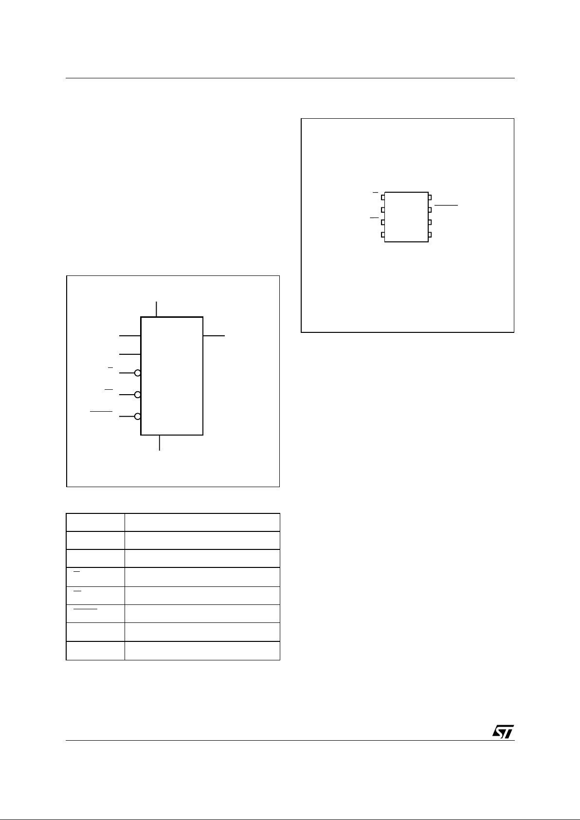
Figure 2. Logi c D iagram
Figure 3. SO and VFQFPN Connections
Note: 1. See page 30 (onwards) for package dimensions, and how
to identify pin-1.
Table 1. Signal Names
AI04080
S
V
CC
M25P20
HOLD
V
SS
W
Q
C
D
1
AI04081B
2
3
4
8
7
6
5
DV
SS
C
HOLDQ
SV
CC
W
M25P20
C Serial Clock
D Serial Data Input
Q Serial Data Output
S
Chip Select
W
Write Protect
HOLD
Hold
V
CC
Supply Voltage
V
SS
Ground

3/34
M25P20
SIGNAL DESCRIPTION
Serial Data Output (Q). This output signal is
used to transfer data serially out of the device.
Data is shifted out on the falling edge of Serial
Clock (C).
Serial Data Input (D). This input signal is used to
transfer data serially into the device. It receives instructions, addresses, and the data to be programmed. Values are latched on the rising edge of
Serial Clock (C).
Serial Clock (C). This input signal provides the
timing of the serial interface. Instructions, addresses, or data present at Serial Data Input (D) are
latched on the rising edge of Serial Clock (C). Data
on Serial Data Output (Q) changes after the falling
edge of Serial Clock (C).
Chip Select (S
). When this input signal is High,
the device is des elected and Serial Data Output
(Q) is at high impedance. Unless an internal Program, Erase or Write Status Register cycle is in
progress, the device will b e in the Standby m ode
(this is not the Deep Power-down mode). Driving
Chip Selec t ( S
) Low enables the device, placing it
in the active power mode.
After Power-up, a falling edge on Chip Select (S
)
is required prior to the start of any instruction.
Hold (HOLD
). The Hold (HOLD) signal is used to
pause any serial communications with the device
without deselecting the device.
During the Hold condition, the Serial Data Output
(Q) is high impedanc e, and Serial D ata Input (D)
and Serial Clock (C) are Don’t Care.
To start the Hold condition, the device must be selected, wit h C hip S e lec t (S
) driven Low.
Write Protect (W
). The main purpose of this in-
put signal is to freeze the size of the area of memory that is protected against program or erase
instructions (as specified by the values in the BP1
and BP0 bits of the Status Register).
M25P20
4/34
SPI MODES
These devices can be drive n by a microcont roller
with its SPI peripheral running in either of the two
following modes:
– CPOL=0, CPHA=0
– CPOL=1, CPHA=1
For these two modes, input dat a is latched in on
the rising edge of Serial Clock (C), and output data
is avai lable from the falling edge of Serial Cloc k
(C).
The difference between the two modes, as shown
in Figure 5, is the clock polarity when the bus master is in Stand-by mode and not transferring data:
– C remains at 0 for (CPOL=0, CPHA=0)
– C remains at 1 for (CPOL=1, CPHA=1)
Figure 4. Bus Master and Memory Devices on the SPI Bus
Note: 1. The Write Protect (W) a nd Hold (HOLD) signals should be driven, High or Low as appropriate.
Figure 5. SPI Modes Sup po r te d
AI03746D
Bus Master
(ST6, ST7, ST9,
ST10, Others)
SPI Memory
Device
SDO
SDI
SCK
CQD
S
SPI Memory
Device
CQD
S
SPI Memory
Device
CQD
S
CS3 CS2 CS1
SPI Interface with
(CPOL, CPHA) =
(0, 0) or (1, 1)
W
HOLD
W
HOLD
W
HOLD
AI01438B
C
MSB
CPHA
D
0
1
CPOL
0
1
Q
C
MSB

5/34
M25P20
OPERATING FEATURES
Page Prog ram m i ng
To program one data byte, two instructions are required: Write Enable (WREN), which is one by te,
and a Page Program (PP) sequence, which consists of four bytes plus data. This is followed by the
internal Program cycle (of duration t
PP
).
To spread this overhead, the Page P rogram (PP)
instruction allows up to 256 bytes to be programmed at a time (changing bits from 1 to 0), provided that they lie in consecutive addresses on the
same page of memory.
Sector Erase and Bulk Erase
The Page Program (PP) instruction allows bits to
be reset from 1 to 0. Before this can be applied, the
bytes of memory need to have been e rased to a ll
1s (FFh). This can be achieved either a sector at a
time, using the Sector Erase (SE) instruction, or
throughout the entire memory, using the Bulk
Erase (BE) instruction. This starts an internal
Erase cycle (of duration t
SE
or tBE).
The Erase instruction must be preceeded by a
Write Enable (WREN) instruction.
Polling During a Write, Program or Erase Cycle
A further improvement in the time to Write Status
Register (WRSR), Program (PP) or Erase (SE or
BE) can be achieved by n ot waiting for the worst
case delay (t
W
, tPP, tSE, or tBE). The Write In
Progress (WIP) bit is provided in the Status Register so that the application program can monitor its
value, polling it to establish when the previous
Write cycle, Program cycle or Erase cycle is complete.
Active Power, Stand-by Power and De ep
Power-Down Modes
When Chip Select (S) is Low, the device is enabled, and in the Active Power mode.
When Chip Select (S
) is High, the device is dis-
abled, but could remain in the Active Power mode
until all internal cycles have completed (Pro gram,
Erase, Write Status Register). The device then
goes in to the Stand-by P ower mode. T he device
consumption drops to I
CC1
.
The Deep Power-down mode is entered when the
specific instruction (the Enter Deep Power-down
Mode (DP) instruction) is executed. The device
consumption drops further to I
CC2
. The device remains in this mode until another specific instruction (the Release from Deep Power-down Mode
and Read Electronic S ignature (RES ) instruction)
is executed.
All other instructions are ignored while the device
is in the Deep Power-down mode. This can be
used as an extra software protection mecha nism,
when the device is not in active use, to protect the
device from inadvertant Write, Program or Erase
instructions.
Status Register
The Status Register contains a num ber of status
and control bits, as shown in Table 5, that can be
read or set (as appropriate) by specific instructions.
WIP bit. The Write In Progress (WIP) bit indicates
whether the memory is busy with a Write Sta tus
Register, Program or Erase cycle.
WEL bit. Th e Write Enable Latch (WEL) bit indicates the status of the internal Write Enable Latch.
BP1, BP0 bits. The Block Protect (BP1, BP0) bits
are non-volatile. They define the size of the area to
be software protected against Program and Erase
instructions.
SRWD bit. The Status Register Write Disable
(SRWD) bit is operated in conjunction with the
Write Protect (W
) signal. The Status Register
Write Disable (SRWD) bit an d Write Protect (W
)
signal allow the device to be put in the Hardware
Protected mode. In this mode, the non-volatile bits
of the Status Register (SRWD, BP1, BP0) become
read-only bits.
M25P20
6/34
Protection Modes
The environments where non-volatile memory devices are used can be v ery noisy. No SPI device
can operate correctly in the presence of excessive
noise. To help combat this, the M25P20 boasts the
following data protection mechanisms:
■ Power-On Reset and an internal timer (t
PUW
)
can provide protection against inadvertant
changes while the power supply is outside the
operating specification.
■ Program, Erase and Write Status Register
instructions are checked that they consist of a
number of clock pulses that is a multiple of
eight, before they are accepted for execution.
■ All instructions that modify data must be
preceded by a Write Enable (WREN) instruction
to set the Write Enable Latch (WEL) bit . This bit
is returned to its reset state by the following
events:
– Power-up
– Write Disable (WRDI) instruction completion
– Write Status Register (WRSR) instruction
completion
– Page Program (PP) instruction completion
– Sector Erase (SE) instruction completion
– Bulk Erase (BE) instruction completion
■ The Block Protect (BP1, BP0) bits allow part of
the memory to be configured as read-only. This
is the Software Protected Mode (SPM).
■ The Write Protect (W) signal, in co-operation
with the Status Register Write Disabl e (SRWD)
bit, allows the Block Protect (BP1, BP0) bits and
Status Register Write Disable (SRWD) bit to be
write-protected. This is the Hardware Protected
Mode (HPM).
■ In addition to the low power consumption
feature, the Deep Power-down mode offers
extra software protection from inadvertant
Write, Program and Erase instructions, as all
instructions are ignored except one particular
instruction (the Release from Deep Powerdown instruction).
Table 2. Protected Area Sizes
Note: 1. The device is ready to accept a Bulk Erase instru ct i on if, and only i f, bo th Block Protec t (BP1, BP0) are 0.
Status Register
Content
Memory Content
BP1 Bit BP0 Bit Protected Area Unprotected Area
0 0 none
All sectors
1
(four sectors: 0, 1, 2 and 3)
0 1 Upper quarter (Sector 3) Lower three-quarters (three sectors: 0 to 2)
1 0 Upper half (two sectors: 2 and 3) Lower half (Sectors 0 and 1)
1 1 All sectors (four sectors: 0, 1, 2 and 3) none
7/34
M25P20
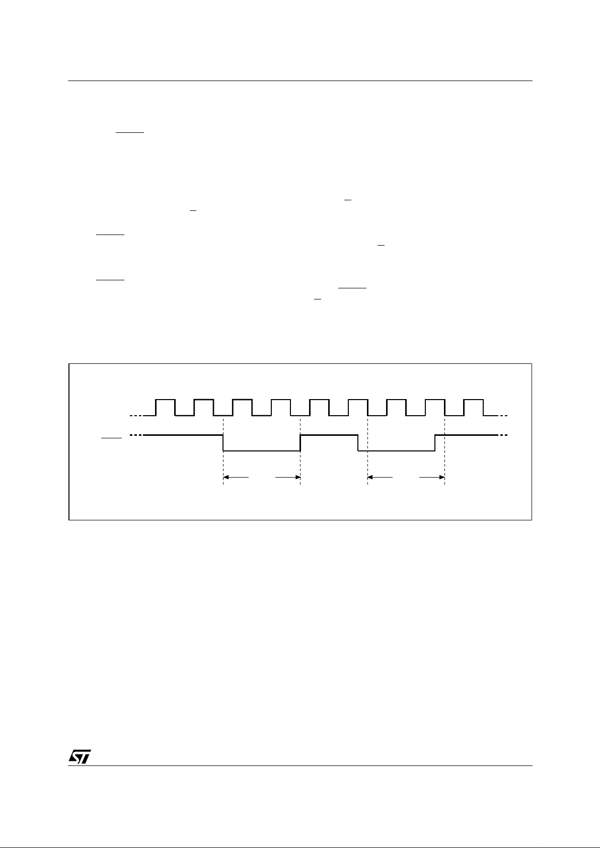
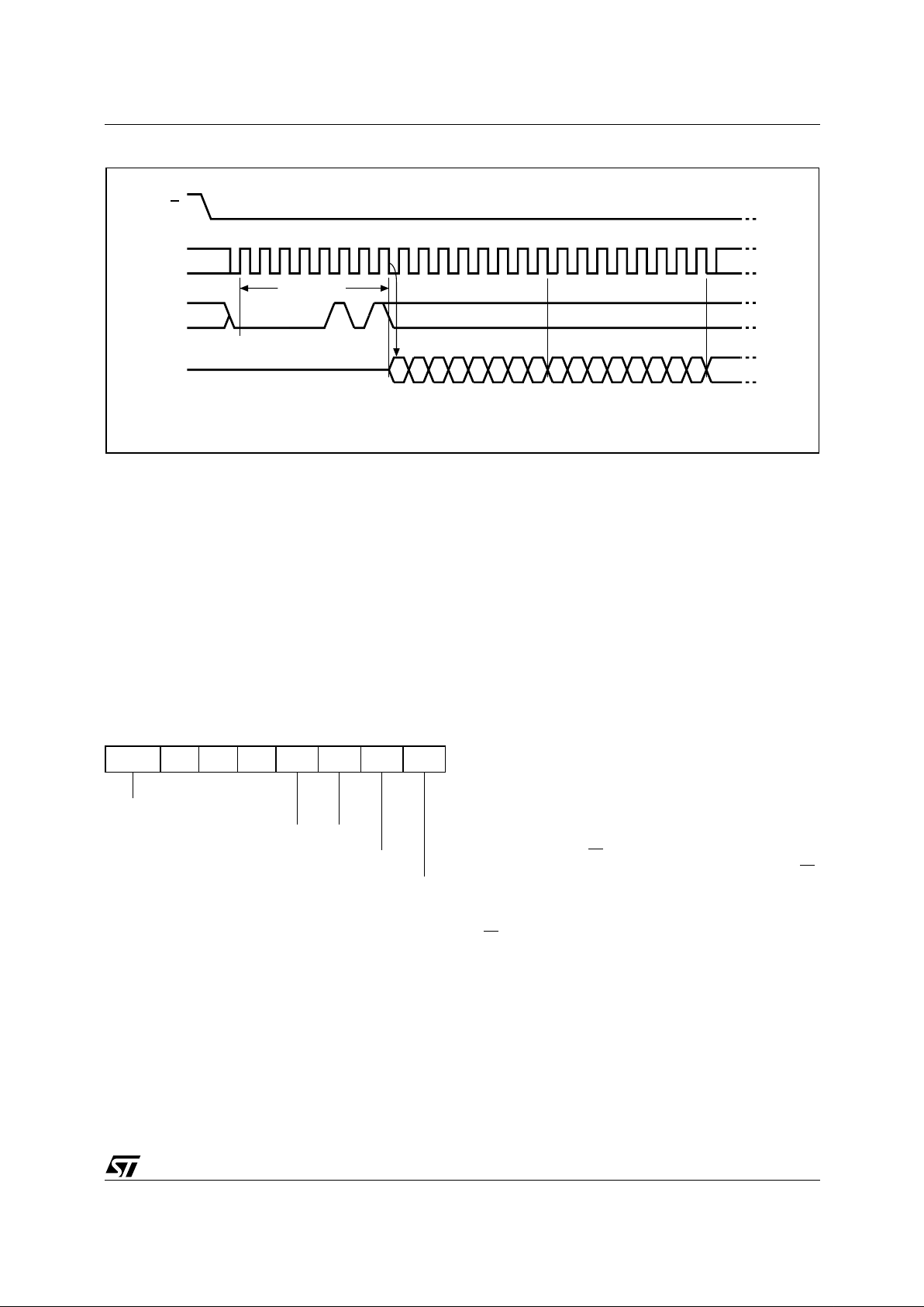
Hold Condition
The Hold (HOLD
) signal is used to pause any serial communications with the device without resetting the clocking sequence. However, taking this
signal Low does not terminate any Write Status
Register, Program or Erase cycle that is currently
in progress.
To enter the Hold condition, the device must be
selecte d, w it h C h ip Select ( S
) Low.
The Hold condition starts on the falling edge of the
Hold (HOLD
) signal, provided that this coincides
with Serial Clock (C) being Low (as shown in Figure 6).
The Hold condition ends on the rising edge of the
Hold (HOLD
) signal, provided that this coincides
with Serial Clock (C) being Low.
If the falling edge does not coincide with Serial
Clock (C) being Low, the Hold condition starts after Serial Clock (C) next goes Low. Similarly, if the
rising edge does not coincide with Serial Clock (C)
being Low, the Hold condition ends after Serial
Clock (C) next goes Low. (This is shown in Figure
6).
During the Hold condition, the Serial Data Output
(Q) is high impedanc e, and Serial D ata Input (D)
and Serial Clock (C) are Don’t Care.
Normally, the device is kept selected, with Chip
Select (S
) driven Low, for the whole duration of the
Hold condition. This is to en sure that the state of
the internal logic remains unchanged from the moment of entering the Hold condition.
If Chip Select (S
) goes High while the d ev ice is in
the Hold condition, this has the effect of reset ting
the internal logic of the device. To restart communication with the device, it is necessary to drive
Hold (HOLD
) High, and then to drive Chip Select
(S
) Low. This prevents the device from going back
to the Hold condition.
Figure 6. Hold Condition Activation
AI02029D
HOLD
C
Hold
Condition
(standard use)
Hold
Condition
(non-standard use)
M25P20
8/34
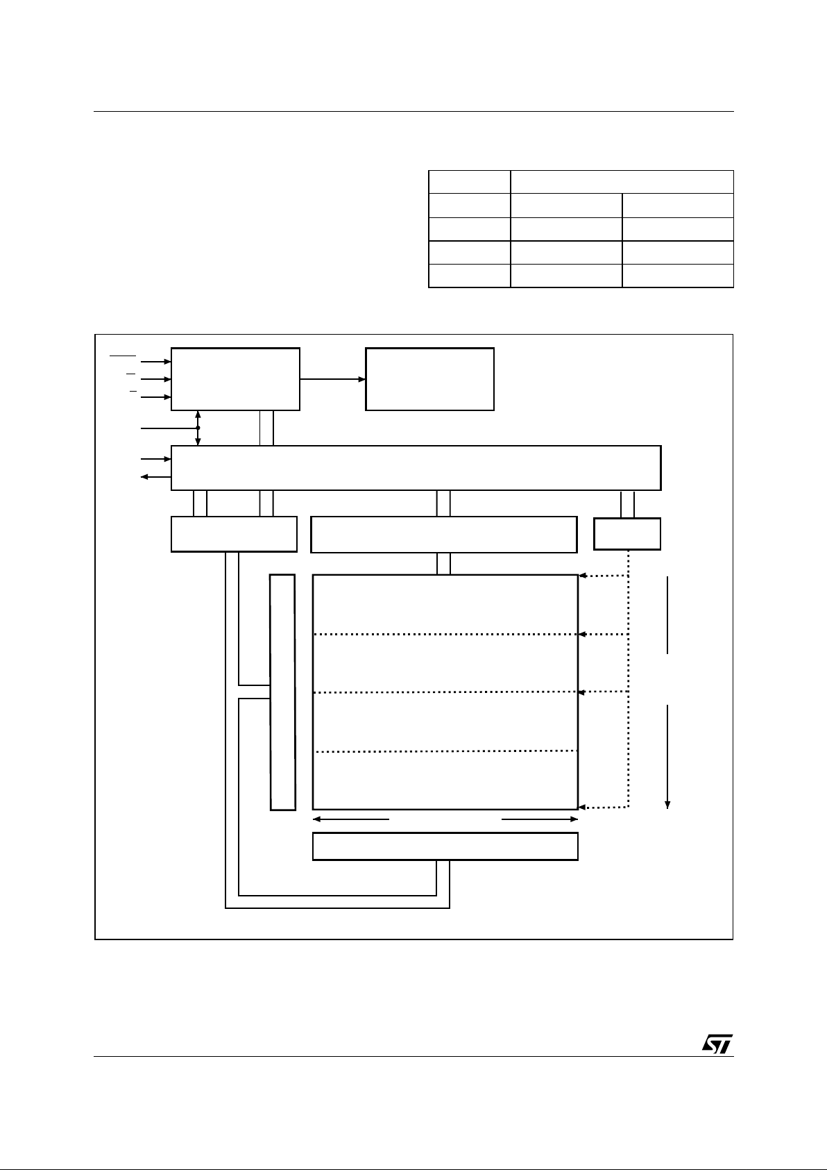
MEMORY OR GANIZATION
The memory is organized as:
■ 262,144 bytes (8 bits each)
■ 4 sectors (512 Kbits, 65536 bytes each)
■ 1024 pages (256 bytes each).
Each page can be individually programmed (bits
are programmed from 1 to 0). The device is Sector
or Bulk Erasable (bits are erased from 0 to 1) but
not Page Erasable.
Table 3. Memory Organization
Figure 7. Block Diagram
Sector Address Range
3 30000h 3FFFFh
2 20000h 2FFFFh
1 10000h 1FFFFh
0 00000h 0FFFFh
AI04079
HOLD
S
W
Control Logic
High Voltage
Generator
I/O Shift Register
Address Register
and Counter
256 Byte
Data Buffer
256 Bytes (Page Size)
X Decoder
Y Decoder
C
D
Q
Status
Register
00000h
10000h
20000h
30000h
3FFFFh
000FFh
Size of the
read-only
memory area
9/34
M25P20
INSTRUCTIONS
All instructions, addresses and data are shifted in
and out of the device, most significant bit first.
Serial Data Input (D) is sampled on the first rising
edge of Serial Clock (C) a fter Chip Select (S
) is
driven Low. Then, the one-byte instruction code
must be shifted in to the device, most significant bit
first, on Serial Data Input (D), each bit being
latched on the rising edges of Serial Clock (C).
The instruction set is listed in Table 4.
Every instruction sequence starts with a one-byte
instruction code. Depending on the instruction,
this might be followed by address bytes, or by data
bytes, or by both or none. Chip Select (S
) must be
driven High after the last bit of the instruction sequence has been shifted in.
In the case of a Read Data Bytes (READ), Read
Data Bytes at Higher Speed (Fast_Read), Read
Status Register (RDSR) or Release from Deep
Power-down, and Read Electronic Signature
(RES) instruction, the shifted-in instruction sequence is followed by a data-out sequ ence. Chip
Selec t (S
) can be driven High after any bit of the
data-out sequence is being shifted out.
In the case of a Page Program (PP), Sector Erase
(SE), Bulk Erase (BE), Write Status Register
(WRSR), Write Enable (WREN), Write Disable
(WRDI) or Deep Power-down (DP) instruction,
Chip Sele ct (S
) must be driven High exactly at a
byte boundary, otherwise the inst ruction is rejected, and is not executed. That is, Chip Select (S
)
must driven High when the number of clock pulses
after Chip Select (S
) being driven Low is an exact
multiple of eight.
All attempts to access the memory array during a
Write Status Register cycle, Program cycle or
Erase cycle are ignored, and the internal Write
Status Register cycle, Program cycle or Erase cycle continues unaffected.
Table 4. Instruction Set
Instruction Description One-byte Instruction Code
Address
Bytes
Dummy
Bytes
Data
Bytes
WREN Write Enable 0000 0110 0 0 0
WRDI Write Disable 0000 0100 0 0 0
RDSR Read Status Register 0000 0101 0 0 1 to
∞
WRSR Write Status Register 0000 0001 0 0 1
READ Read Data Bytes 0000 0011 3 0 1 to
∞
FAST_READ Read Data Bytes at Higher Speed 0000 1011 3 1 1 to
∞
PP Page Program 0000 0010 3 0 1 to 256
SE Sector Erase 1101 1000 3 0 0
BE Bulk Erase 1100 0111 0 0 0
DP Deep Power-down 1011 1001 0 0 0
RES
Release from Deep Power-down,
and Read Electronic Signature
1010 1011
0 3 1 to
∞
Release from Deep Power-down 0 0 0
M25P20
10/34
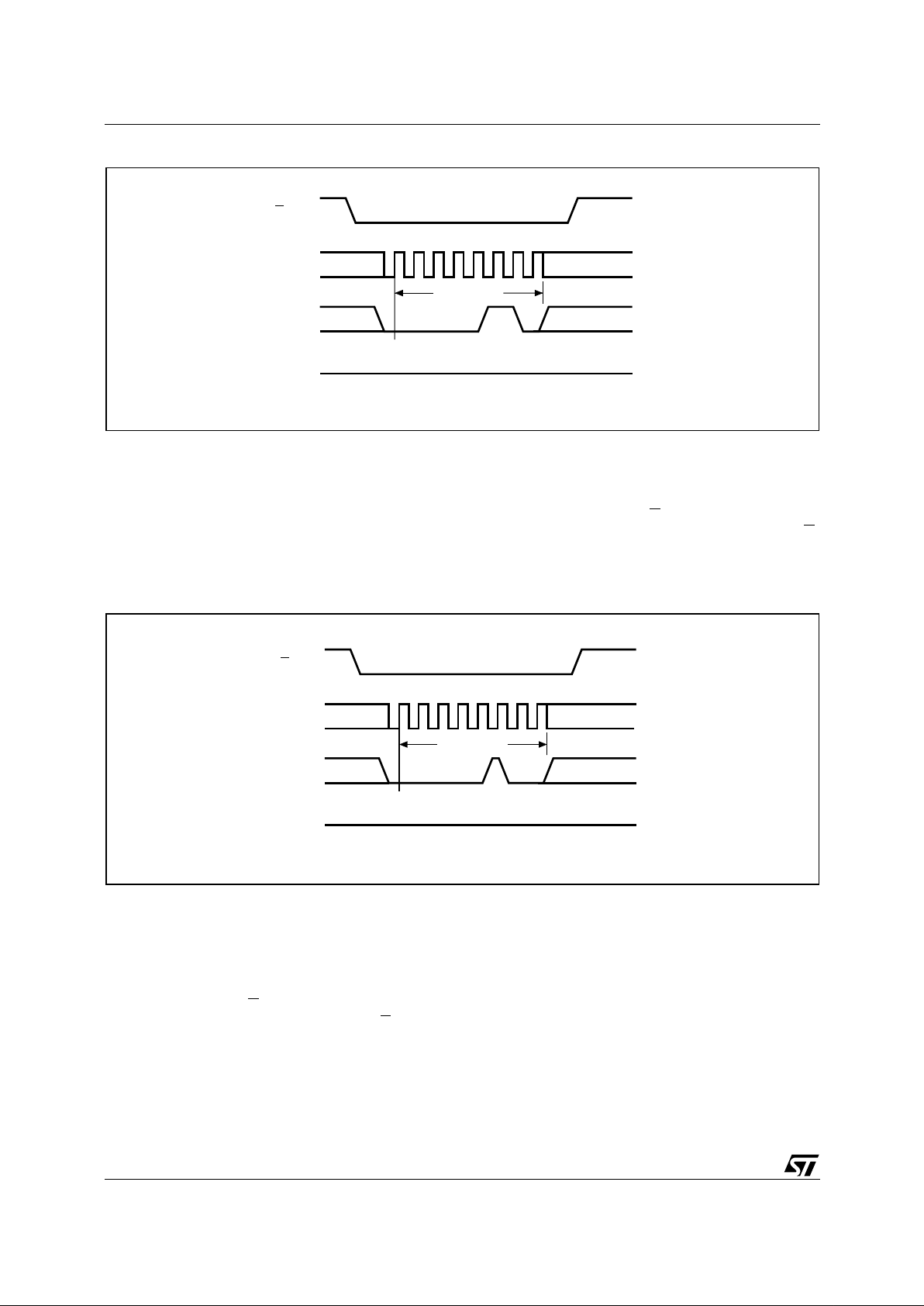
Figure 8. Write Enable (WREN) Instruction Sequenc e
Write Enable (WREN)
The Write Enable (WREN) instruction (Figure 8)
sets the Write Enable Latch (WEL) bit.
The Write Enable Latch (WEL) bit must be set prior to every Page Program (PP), Sector Erase
(SE), Bulk Erase (BE) and Write Status Register
(WRSR) instruction.
The Write Enable (WREN) instruction is entered
by driving Chip Select (S
) Low, sending the in-
struction code, and then driving Chip Select (S
)
High.
Figure 9. Write Disable (WRDI) Instruction Sequence
Write Disable (WRDI)
The Write Disable (WRDI) instruction (Figure 9)
resets the Write Enable Latch (WEL) bit.
The Write Disable (WRDI) instruction is entered by
driving Ch ip Select (S
) Low, sending the instruc-
tion code, and then driving Chip Select (S
) High.
The Write Enable Latch (WEL) bit is reset under
the following conditions:
– Power-up
– Write Disable (WRDI) instruction completion
– Write Status Register (WRSR) instruction com-
pletion
– Page Program (PP) instruction completion
– Sector Erase (SE) instruction completion
– Bulk Erase (BE) instruction completion
C
D
AI02281E
S
Q
21 34567
High Impedance
0
Instruction
C
D
AI03750D
S
Q
21 34567
High Impedance
0
Instruction
11/34
M25P20
Figure 10. Read Status Register (RDSR) Instruction Sequence and Data-Out Sequence
Read Status Register (RDSR)
The Read Status Register (RDSR) instruction allows the Status Register to be read. The Status
Register may be read at any time, even while a
Program, Erase or Write Status Register cycle is in
progress. When one of these cycl es i s in progress,
it is recommended to check the Write In Progress
(WIP) bit before sending a new instruction to the
device. It is also possible to read the Status Register continuously, as shown in Figure 10.
Table 5. Status Register Format
The status and cont rol bits of t he Stat us Register
are as follows:
WIP bit. The Write In Progress (WIP) bit indicates
whether the memory is busy with a Write Status
Register, Program or Erase cycle. When set to 1,
such a cycle is in progress, when reset to 0 no
such cycle is in progres s.
WEL bit. Th e Write Enable Latch (WEL) bit indicates the status of the internal Write Enable Latch.
When set to 1 the internal Write Enable Latch is
set, when set to 0 t he i nte rnal W rite E nabl e Latch
is reset and no Write S tatus Reg ister, Pr ogram or
Erase instruction is accepted.
BP1, BP0 bits. The Block Protect (BP1, BP0) bits
are non-volatile. They define the size of the area to
be software protected against Program and Erase
instructions. These bits are written with the Write
Status Register (WRSR) instruction. When one or
both of the Block Protec t (B P 1, B P0 ) bits i s s et t o
1, the relevant memory area (as defined in Table
2) becomes protected against Page Program (PP)
and Sector Erase (SE) instructions. The Block
Protect (BP1, BP0) bits can be written provided
that the Hardware Protect ed mode has not been
set. The Bulk Erase (BE) instruction is executed if,
and only if, both Block Protect (BP1, BP0) bits are
0.
SRWD bit. The Status Register Write Disable
(SRWD) bit is operated in conjunction with the
Write Protect (W
) signal. The Status Register
Write Disable (SRWD) bit an d Write Protect (W
)
signal allow the device to be put in the Hardware
Protected mode (when t he Status Register Write
Disable (SRWD) bit is set to 1, and Write Protect
(W
) is driven Low). In this mode, the non-volatile
bits of the Status Register (SRWD, BP1, BP0) become read-only bits and the Write Status Register
(WRSR) instruction is no longer accepted for execution.
C
D
S
21 3456789101112131415
Instruction
0
AI02031E
Q
7 6543210
Status Register Out
High Impedance
MSB
7 6543210
Status Register Out
MSB
7
b7 b0
SRWD 0 0 0 BP1 BP0 WEL WIP
Status Register Write Protect
Block Protect Bits
Write Enable Latch Bit
Write In Progress Bit
 Loading...