


SPEECH AND 14 MEMORYDIALER WITH LED DRIVER
SPEECH CIRCUIT
2 TO 4 WIRESCONVERSION
PRESENTTHE PROPER DC PATH FOR THE
LINE CURRENT AND THE FLEXIBILITY TO
ADJUST IT AND ALLOW PARALLEL PHONE
OPERATION
PROVIDES SUPPLY WITH LIMITED CURRENT FOREXTERNALCIRCUITRY
SYMMETRICAL HIGH IMPEDANCE MICROPHONE INPUTS SUITABLE FOR DYNAMIC
ELECTRET OR PIEZOELECTRIC
TRANSDUCER
ASYMMETRICAL EARPHONE OUTPUT
SUITABLEFOR DYNAMICTRANSDUCER
LINELOSS COMPENSATION
INTERNAL MUTING TO DISABLE SPEECH
DURING DIALING
LIGHTED DIAL LED CONSUMING 25% OF
LINE CURRENT
DIALER CIRCUIT
32 DIGITS FOR LAST NUMBER REDIAL
BUFFER
18 DIGITS FOR 13 MEMORY REDIAL
ALLOW MIXED MODE DIALING IN EITHER
TONE OR PULSEMODE
PACIFIER TONE PROVIDES AUDIBLE INDI-
CATION OF VALID KEY PRESSED IN A
BUZZER OR/AND IN THE EARPHONE
TIMEDPABX PAUSE
FLASHINITIATESTIMEDBREAK:585ms.
CONTINUOUS TONE FOR EACH DIGIT UN-
TIL KEY RELEASE
USES INEXPENSIVE 3.579545MHz CE-
RAMIC RESONATOR
POWERED FROM TELEPHONE LINE, LOW
OPERATING VOLTAGE FOR LONG LOOP
APPLICATION
SO28
ORDERING NUMBER: L3916AD
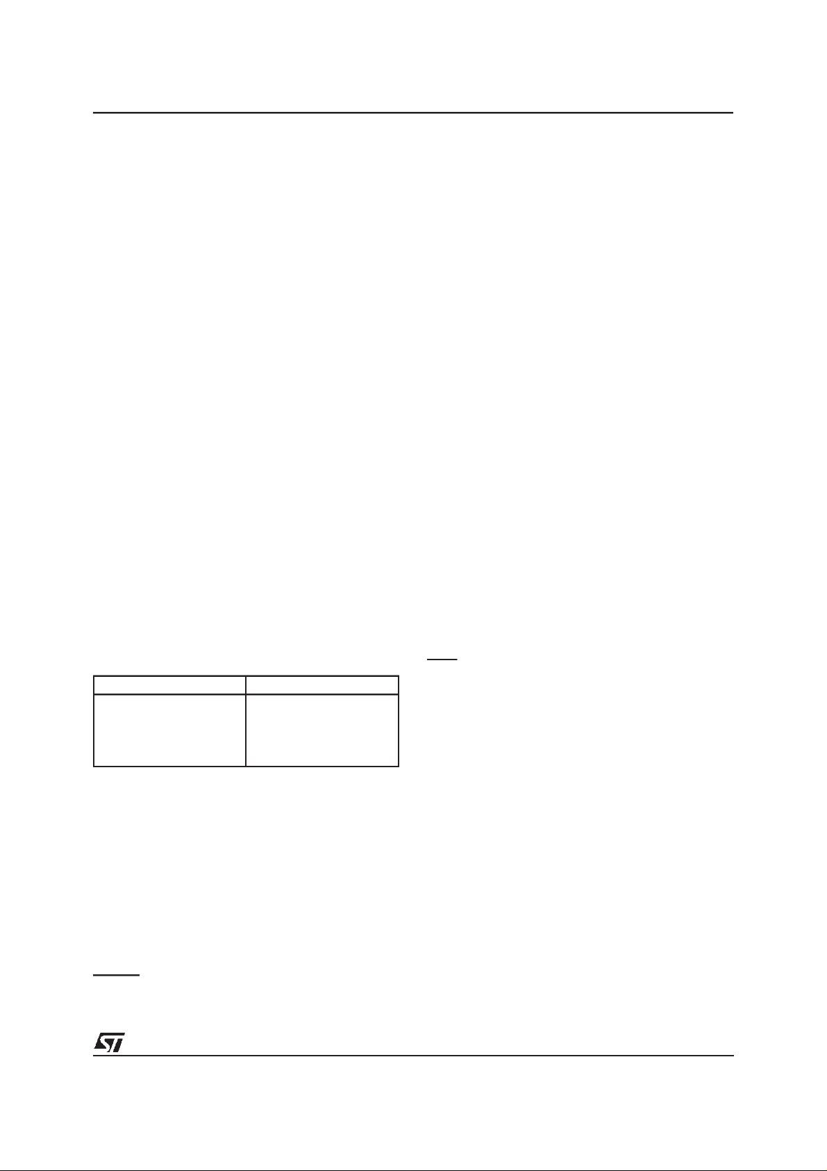
PIN CONNECTION
(Top view)
KEYPADCONFIGURATION
L3916A
DESCRIPTION
The device consists of the speech and the dialer.
It provides the DC line interface circuit that terminates the telephone line, analog amplifier for
speech transmission and necessary signals for
either DTMF or loopdisconnect(pulse)dialing.
March 2000
Note: PAUSE/LND:
PAUSE and LND functions are sharing the same key with different
sequence.Hereafter, PAUSEandLND keysarereferring tothe same
key.
1/14

L3916A
BLOCK DIAGRAM
DESCRIPTION
(continued)
When mated with a tone ringer, a complete telephone can be producedwith just two ICs.
The DC line interface circuit develops its own line
voltage across the device and it is adjustable by
external resistor to suit different country’s specification.
The speech network provides the two to four
wires interface, electronic switching between dialing and speech and automatic gain control on
transmit and receive.
The dialing network buffers up to 32 digits into the
LND memory that can be later redialed with a single key input. Additionally, another 13 memories
(including 3 emergency memories) of 18 digits
memory is available. Users can store all 13 signalling keys and access several unique functions
with single key entries. These functions include:
Pause/Last Number Dialed (LND), Softswitch,
Flash.
2/14
The FLASH key simulates a timed hook flash to
transfer calls or to activate other special features
providedby the PABX or central office.
The PAUSE key storesa timedpause in the number sequence.Redial is then delayed until an outside line can be accessed or some other activity
occurs before normal signaling resumes.
A LND key input automatically redials the last
numberdialed.
FUNCTIONPIN DESCRIPTION
C1, C2, C3, C4, R5, R4, R3, R2, R1
Keyboards inputs. Pins 1, 2, 3, 4, 24, 25, 26, 27,
28. The one chip phone interfaces with either the
standard 2-of-9 with negative common or the single-contact(FormA) keyboard.
L3916A
FUNCTIONPIN DESCRIPTION
(continued)
A valid keypad entry is either a single Row connected to a single Column or GND simultaneously
presented to both a single Row and a single Colunm.
In its quiescent or standby state, during normal
off-hook operation, either the Rows or the Columns are at logic level 1 (V
). Pulling one input
DD
low enables the on chip oscillator. Keyboard
scanningthen begins.
Scanning consists of Rows and Columns alternately switching high through on chip pullups. After both a Row and Column key have been detected, the debounce counter is enabled and any
noise (bouncing contacts, etc) is ignored for a debounce period (TKD) of 32ms. At this time, the
keyboardis sampled and if boththe Row and Column information are valid, the information is buffered into the LND location. After scanning starts,
the row and column inputs will assume opposite
states.
In the tone mode, if two or more keys in the same
row or if two or morekeys in the same column are
depressed a single tone will be output. The tone
will corresponds to the row or column for which
the two keys were pushed. This feature is for testing purposes, and single tone will not be redialed.
Also in the tone mode, the output tone is continuous in the manual dialing as long as the key is
pushed. The output tone duration follows the Table 1. When redialing in the tone mode, each
DTMF output has 100ms duration, and the tone
separation (inter signal delay) is 100ms.
pulseoutput pin is in high impedanceandonceoffhooked,itwillbepulledhighby externalresistor.
MODE/PACIFIERTONE
Input (MODE). Pin 7. MODE determines the dialer’s default operating mode. When the device is
powered up or the hookswitch input is switched
from on-hook (V
determines the signalling mode. A V
) to off-hook(GND), the default
DD
DD
connection defaults to tone mode operation and a GND
connectiondefaultsto pulse mode operation.
When dialing in the pulse mode, a softswitch feature will allow a change to the tone mode whenever the * key is depressed. Subsequent* key inputs will cause the DTMF code for an * to be
dialed.. The softswitch will only switch from pulse
to tone.After returning to on-hook and back to offhook, the phone will be in pulse mode. Redial by
the LND key or the MEM key will repeat the softswitch.
Output (PACIFIER TONE). Pin 7. In pulse mode,
all valid key entries activate the pacifier tone. In
tone mode, any non DTMF entry (FLASH,
PROG, PAUSE, LND, MEM, E1, E2 and E3), activates the pacifier tone. The pacifier tone provides
audible feedback, confirming that key has been
properly entered and accepted. It is a 500Hz
square wave activated upon acceptance of valid
key input after the 32ms debounce time. The
square wave terminates after a maximum of
75ms or when the valid key is no longer present.
The pacifier tone signal is simultaneously sent to
earphone and the buzzer. The buzzer can be removedwithout affecting this function.
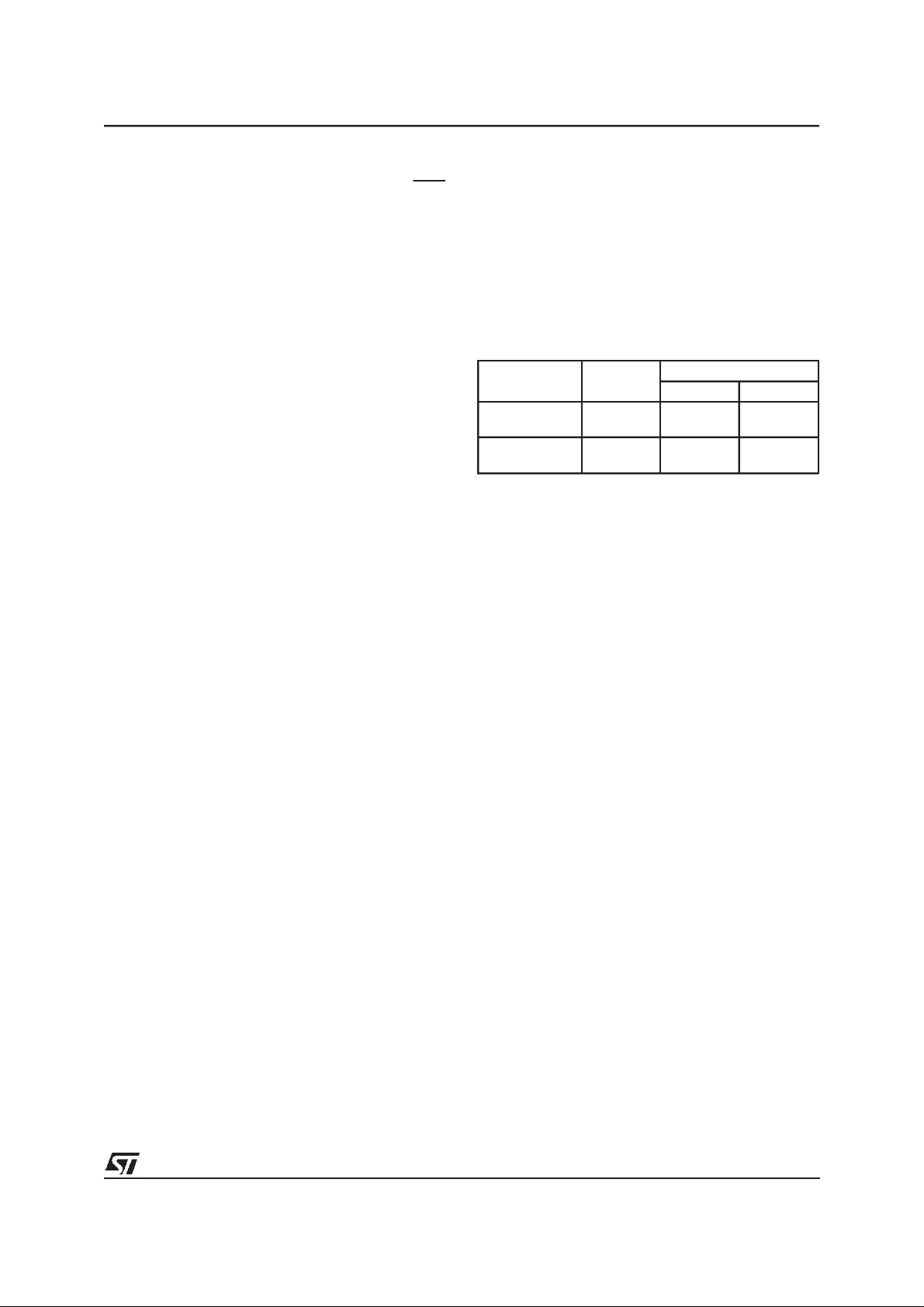
Table 1:
Key-Push Time, T Tone Output
T<= 32ms
32ms < = T < = 100ms +
Tkd
T > = 100ms + Tkd
OutputToneDuration
No output, ignored by
one chip phone.
100ms Duration
Output Duration = T - Tkd
OSC
Output. Pin 5. Onlyone pin is needed to connect
the ceramic resonator to the oscillator circuit. The
other end of the resonator is connected to GND
(pin 8). The nominal resonator frequency is
3.579545MHz and any deviation from this standard is directly reflected in the Tone output frequencies. The ceramic resonator provides the
time reference for all circuit functions. A ceramic
resonator with tolerance of ±0.25% is recommended
PULSE
Output. Pin 6. This is an output consisting of an
open drain N-Channel device. During on-hook,
HKS
Input.Pin 8. This is the hookswitchinputto the one
chip phone. This is a high impedance input and
mustbe switched highfor on-hookoperationorlow
for off-hook operation. A transition on this input
causes the on chip logic to initialize, terminating
anyoperationinprogressat the time. The signaling
mode defaults to the mode selected at pin 7. Figures1and2illustrate thetimingforthispin.
GND
Pin 9 is the negative line terminal of the device.
This is the voltage reference for all specifications.
RXOUT, GRX, RXIN
RXOUT(pin 10), GRX (pin 11) and RXIN (pin 12).
The receive amplifier has one input RXIN and a
non inverting output RXOUT. Amplification from
RXIN to RXOUT is typically 31dB and it can be
adjusted between 11dB and 41dB to suit the sensitivity of the earphone used. The amplification is
proportionalto the external resistor connectedbetween GRX and RXOUT.
3/14

L3916A
FUNCTIONPIN DESCRIPTION
(continued)
IREF
Pin 13. An external resistor of 3.6kOhm connected between IREF and GND will set the internal current level. Any changeof this resistor value
will influence the microphone gain, DTMF gain,
earphone gain and sidetone.
V
CC
Pin 14, VCCis the positive supply of the speech
network. It is stabilized by a decoupling capacitor
between V
and GND. The VCCsupply voltage
CC
may also be used to supply external peripheral
circuits.
LED
Pin 15. Lighted dial indicator.The LED connected
to this pin will light up when the telephone is offhook andconsuming 25% of theline current.
I
LINE
Pin 16. A recommended external resistor of
20ohm is connected between I
LINE
and GND.
Changingthis resistor value will have influenceon
microphonegain, DTMF gain, sidetone, maximum
output swing on LN and on the DC characteristics
(especiallyin the low voltageregion).
is 40dB. Final ouput level on LN can be adjusted
via the external resistor connected between
GDTMF and GND through a decoupling capacitor. A confidence tone is sent to the earphone
during tone dialing. The attenuation of the confidencetone from LN to Vear is –32dB typically.
V
DD
Pin 23. VDDis the positive supply for the dialing
network and must meet the maximum and minimum voltage requirements.
DEVICEOPERATION
During on-hook all keypad inputs are high impedance internally and it requires very low currentfor
memory retention. At anytime, Row and Column
inputs assume opposite states at off-hook. The
circuit verifies that a valid key has been entered
by alternately scanning the Row and Column inputs. If the input is still valid following 32ms of debounce, the digit is stored into memory, and dialing begins after a pre-signal delay of
approximately 40ms (measured from the initial
key closure). Outputtone duration is shown in Table1.
The device allows manual dialing of an indefinite
number of digits, but if more than 32 digits are dialed, it will ”wrap around”.That is, the extra digits
beyond 32 will be stored at the beginning of LND
buffer, and the first 32 digits will no longer be
availableforredial.
LN
Pin 17. LN is the positive line terminal of the device.
REG
Pin 18. The internal voltage regulator has to be
decoupled by a capacitor from REG to GND. The
DC characteristicscan be changed with an external resistor connected between LN and REG or
between REG and I
LINE
.
GTX, MIC–, MIC+
GTX (pin 19), MIC– (pin 20) and MIC+ (pin 21).
The one chip phone has symmetrical microphone
inputs.Theamplificationfrommicrophoneinputsto
LN is 51.5dB and it can be adjustedbetween 43.5
and 51.5dB.Theamplification is proportionaltoexternalresistorconnectedbetweenGTXandREG.
GDTMF
Pin 22. When the DTMF input is enabled, the microphoneinputs and the receiveamplifier input will
be muted and the dialing tone will be sent to the
line. The voltage amplification from GDTMF to LN
Table 2: DTMF Output Frequency
Key Input
ROW 1
ROW 2
ROW 3
ROW 4
COL 1
COL 2
COL 3
Stadard
Frequency
697
770
852
941
1209
1336
1477
Actual
Frequency
699.1
766.2
847.4
948.0
1215.9
1331.7
1471.9
% Deviation
+0.31
–0.49
–0.54
+0.74
+0.57
–0.32
–0.35
NORMAL DIALING
D1 D2 D3 ....etc
Normal dialing is straighforward, all keyboard entries will be stored in the buffer and signaled in
succession.
PROGRAMMING AND REPERTORY DIALING
To program, enter the following:
PROG D1 D2 D3. . . Dn MEM (Location0-9)
or
PROG D1 D2.. . .Dn E1-E3
During programming,dialingis inhibited.
4/14
L3916A
FUNCTIONPIN DESCRIPTION
(continued)
To dial a number from repertory memory (HKS
must be low), enter the following:
MEM (Location 0-9) or E1-E3
To save the last number dialed, enter the following:
PROG MEM (location 0-9) or E1-E3
HOOK FLASH
D1 FLASH D2 ...etc
Hook flash may be entered into the dialed sequence at any point by keying in the function key,
FLASH. Flash consists of a timed break of
585ms, 300ms or 100ms dependingon the Mask
option. When a FLASH key is pressed, no further
key inputs will be accepted until the hookflash
function has been dialed. The key input following
a FLASH will be stored as the initial digit of the
new number, overwriting the number dialed before theFLASH,unless it isanotherFLASH.
FLASH key pressed immediatelyafter hookswitch
or LND will not clear the LND buffer unless digits
are enteredfollowingthe FLASH key.
Example:
FLASH
LND not cleared
LND FLASH
LND not cleared
LND FLASH D1 D2
LND bufferwill contain D1, D2
PAUSE/LASTNUMBER DIALED
If the PAUSE/LND key is pressed right after off
hook or FLASH key, it is considered as LND, if it
is pressed after a digit, it will be considered as
PAUSE.
LAST NUMBEREDDIALED
OFF-HOOKPAUSE/LNDor FLASH PAUSE/LND
Last number dialing is accomplished by entering
the PAUSE/LND key.
PAUSE
OFF-HOOK D1 PAUSE/LND D2 ...etc
A pause may be enteredinto the dialed sequence
at any point by keying in the special function key,
PAUSE/LND. Pause inserts a 3.1 second delay
into the dialing sequence. The total delay, including pre-digit and post-digit pauses is shownin Table 3.
Table 3: SpecialFunction Delays
Each delay shown below represents the time re-
quired after the special function key is depressed
until a new digit is dialed. The time is considered
”FIRST” key if all previous inputs have been completelydialed. The time is considered”AUTO”if in
redial,or if previous dialling is still in progress.
Function First/Auto
SOFTSWITCH FIRST
AUTO
PAUSE FIRST
AUTO
Delay (seconds)
Pulse Tone
0.2
1.0
2.6
3.4
3.0
3.1
SOFTSWITCHFUNCTIONUSING TONE/PULSE
MODE SWITCH
When dialing in Pulse mode after off-hook,
switching TONE/PULSE mode switch from Pulse
to Tone will cause the device to change the signaling mode into tone signal and store the softswitch function in the LND memory for redial. To
redial the softswitch function(mixed mode dialing)
in the pulse mode after going on-hook and back
to off-hook,you have to switch the TONE/PULSE
modeswitch back to pulse mode either before going on-hook or after off-hook or during on-hook.
Subsequent mode change from Tone to Pulse will
change the signaling mode to pulse dialing sequence but this mode change will not be stored in
.the LND memory.
When dialing in Tone mode after off-hook, a
switching of TONE/PULSE mode Switch from
Tone to Pulse will cause the device to changethe
signaling mode into pulse mode but this mode
change will not be stored in the LND memory.
When LND key is pressed in Tone mode after going off-hook, the device will output all tone signals.
A pacifier tone of 75msis providedafter 32ms debounce time when switching from Pulse to Tone
mode.
Redial by the LND key will repeat the mixed dialing sequence in Pulse mode.
5/14

L3916A
Figure 1:
Tone Mode Timing
Figure 2: PulseMode Timing
6/14

L3916A
ABSOLUTE MAXIMUM RATINGS
Symbol Parameter Value Unit
V
LN
I
LN
V
DD
V
T
amb
T
stg
P
tot
Positive Line VoltageContinuous 12 V
Line Current 140 mA
Logic Voltage 7.0 V
Maximum Voltage on Any Pin GND(-0.3) VDD(+0.3) V
I
Operating Temperature Range -25 to +75
Storage Temperature -40 to 125 °C
Total Power Dissipation 700 mW
C
°
ELECTRICAL CHARACTERISTICS (IL= 10 to 120mA; VDD= 3V; f = 1KHz; T
=25°C, unless other-
amb
wise specified)
Symbol Parameter Test Condition Min. Typ. Max. Unit Fig.
V
LN
V
DD
I
DD
I
CC
I
LED
V
MR
I
MR
I
S
I
PL
I
PO
V
IL
V
IH
G
TX
A
GTX
D
TX
N
TX
Z
MIC
Line Voltage IL= 4mA
I
= 15mA
L
I
= 120mA
L
R
= 68K
Ω
A
R
= 39KΩIL= 15mA
B
Logic Voltage) TONE MODE
PULSE MODE
Supply Current Into V
DD
TONE MODE
PULSE MODE
Supply Current Into V
CC
IL= 15mA 1.30 mA 3
Supply Current to LED IL= 15mA
I
= 120mA
L
I
= 15mA
L
3.15 3.50
3.2
4.1
2.50
2.20
600
400
30
2.50
3.85
7.0
6.00
6.00
4
Memory Retention Voltage 1.50 V 4
Memory Retention Current 1.00
Off-HookStand-byCurrent VDD= 4.0V 150 250
Pulse Output Sink Current VO= 0.5V 1.00 3.00 mA 3
Pacifier Tone Sink/Source
Current
HKS, Mode, Keyboard Inputs
VO= 0.5V (Sink)
V
= 2.5V (Source)
O
1
0.6
3
1.0
0.3xV
Low
HKS,Mode, Keyboard Inputs
0.7xV
DD
High
Transmit Gain V
Transmit Gain Variation with
R
GTX
= 2mVrms
mic
I
= 15mA R
L
I
= 60mA; R
L
IL= 15mA
V
= 2mVrms
mic
R
= 43K
GTX
R
= 27KΩ
GTX
Ω
GTX
GTX
= 68K
= 68K
Ω
Ω
50.0
44.5
–8
51.5
46.5
53.0
48.5dBdB
0dB
–4
–8
Transmit Distortion IL= 15mA VLN= 1Vrms 2 % 6
Transmit Noise IL= 15mA; V
= 0V –72 dBmp 6
mic
Microphone Input Impedance 65 K
V
V
V
V
V
V
V
A
µ
µA
mAmA3
A4
µ
A3
µ
mAmA3
V-
DD
V-
dB
dB
Ω
3
3
3
6
6
7/14

L3916A
ELECTRICALCHARACTERISTICS (continued)
Symbol Parameter Test Condition Min. Typ. Max. Unit Fig.
G
C
V
DTMF
DTMF
DTMF
DTMF Gain IL=15mA,R
Confidence Tone Level
V
ear/VLN
DTMF Level on the line
High Frequency Group
R
= 2.25KΩ,
DTMF
C
= 22nF –8
DTMF
Low Frequency Group
P
Pre-emphasis 1.0 2 3 dB 7
EI
DIS DTMF Output Distortion 5 8 % 7
Z
G
A
D
DTMF
GRX
DTMF Att. pin Impedance 32 K
Receive Gain V
RX
= 5mVrms, Re= 300
inp
R
= 100KΩ
GRX
I
= 15mA
L
I
= 60mA
L
ReceiveGain Variation IL=15mA, Re= 300
R
= 10KΩ
GRX
R
= 300K
GRX
Reveive Distortion IL= 15mA; R
RX
Re = 150
Re= 300
Ω,
Re= 450Ω,VC= 0.55V
N
Z
OUT
V
Recei veNoise IL= 15mA RL= 300
RX
R
GRX
= 100KΩ V
Receive Output Impedance IL= 15mA 35
Pacifier Tone Level on
PT
IL= 15mA; Rp=
Earphone
KEYBOARD INTERFACE
TKD
FKS
KRU
KRD
Keypad Debounce Time
Keypad Scan Frequency
Keypad Pullup Resistance
Keypad Pulldown Resistance
PULSE MODE
TPT
FPT
PR
TB
TM
IDP
PDP
Pacifier Tone Duration
Pacifier Tone Frequency
Pulse Rate
Break Time
Make Time
Inter Digit Pause
Predigit Pause
TONE MODE
TRIS
TR
TPSD
TISD
TDUR
t
HFP
Notes:
1. All inputsunloaded. Quiescent mode (oscillator off).
2. Pulse outputsink current forV
3. Pacifier tone sink current for V
4. Memory retention voltage is the point where memory is guaranteed butcircuit operation is not. Proper memory retention is guaranteedif
either the minimum IMR is provided or the minimum VMR.The design does not have to provide boththe minimum currentand voltage
simultaneously.
Tone Output Rise Time
Tone Signalling Rate
Pre Signal Delay
Inter Signal Delay
Tone Output Duration
Hook Flash Timing 585 ms
= 0.5V.
OUT
= 0.5V.Source current for V
OUT
= 2.25KΩ 38 40 42 dB 7
DTMF
–34 –32 –30 dB 7
–6
–10
–8
Ω
29.52431.02632.528dB
Ω
–20
+10 dB
–20
Ω
GRX
Ω,
VC= 0.25V
VC= 0.45V
∞
R
= 430K
p
= 100K
Ω
=0V
inp
Ω
rms
rms
rms
+10
200 8
60
600
32
250
100
500
75
500
10
60
40
820
50
5
40
100
100
= 2.5V.
OUT
–4–6dBm
dBm
Ω
dB
dB
dB
%
2
%
2
%
2
µV
Ω
mVrm s
mVrms
ms
Hz
KΩ
Ω
ms
Hz
PPS
ms
ms
ms
ms
5ms
1/s
ms
ms
ms
7
8
8
8
8
8
8/14

TEST CIRCUITS
Figure 3.
L3916A
IDD
470nF
300Ω
Re
100µF
RDTMF
PULSE
TONE
10µF
ICC
470KVDD
2.25K
GDTMF
22nF
SW1 GND
3.58MHz
100K
100K
RGRX
3.6K
620ΩV1
VDD
PULSE
OSC
MODESW2
/PT
HKS
RXOUT
GRX
IREF
VCC
RGIN
100nF
22
23
6
5
7
8
9
10
11
13
14
12
4
3
2
1
28
27
26
25
24
21
20
19
18
17
15
16
C4
C3
C2
C1
123
R1
456
R2
789
R3
R4
*
E1 E2 E3 MEM
R5
MIC+
2.2K 1µF
MIC-
GTX
RGTX 68K
REG
LN
LED
ILED
ILINE
FLASH
PROG
P/LND
0#
1µF
4.7µF
RB 130K
390Ω 3.9K
390Ω20Ω
RA
ICC =
VLN
D95TL162
V1
VCC
100µF
IL
600Ω
Figure 4.
VMR
470nF
IMR
300Ω
Re
100µF
470K
PULSE
TONE
10µF
2.25K
GDTMF
22nF
SW1 GND
620Ω 100nF
3.58MHz
100K
RGRX
3.6K
VDD
PULSE
OSC
MODESW2
/PT
HKS
RXOUT
GRX
IREF
VCC
RGIN
22
23
6
5
7
8
9
10
11
13
14
12
4
3
2
1
28
27
26
25
24
21
20
19
18
17
15
16
C4
C3
C2
C1
123
R1
456
R2
789
R3
R4
*
E1 E2 E3 MEM
R5
MIC+
2.2K 1µF
MIC-
GTX
RGTX
REG
LN
LED
ILED
ILINE
FLASH
PROG
P/LND
0#
1µF
4.7µF
390Ω 3.9K
390Ω20Ω
130K
D95TL163
9/14

L3916A
TEST CIRCUITS(continued)
Figure 5.
470nF
300Ω
Re
100µF
PULSE
TONE
10µF
D95TL164
2.25K
GDTMF
22nF
470K
3.58MHz
100K
SW1 GND
RXOUT
RGRX
3.6K
620Ω 100nF
VDD
PULSE
OSC
MODESW2
/PT
HKS
GRX
IREF
VCC
RGIN
22
23
6
5
7
8
9
10
11
13
14
12
C4
4
C3
3
C2
2
C1
1
28
27
26
25
24
21
20
19
18
17
15
16
R1
R2
R3
R4
R5
MIC+
MIC-
GTX
REG
LN
LED
ILED
ILINE
123
FLASH
456
789
*
E1 E2 E3 MEM
RGTX
PROG
P/LND
0#
Imic
1.2V
4.7µF
390Ω 3.9K
390Ω20Ω
ZMIC =
130K
1.2V
Imic
Figure 6.
IDD
470nF
Re
100µF
470KVDD
PULSE
TONE
10µF
2.25K
GDTMF
22nF
SW1 GND
620Ω 100nF
3.58MHz
100K
100K
RGRX
3.6K
VDD
PULSE
OSC
MODESW2
/PT
HKS
RXOUT
GRX
IREF
VCC
RGIN
22
23
6
5
7
8
9
10
11
13
14
12
4
3
2
1
28
27
26
25
24
21
20
19
18
17
15
16
C4
C3
C2
C1
123
R1
456
R2
789
R3
R4
*
E1 E2 E3 MEM
R5
MIC+
2.2K 1µF
MIC-
GTX
RGTX 88K
REG
LN
LED
ILED
390Ω 3.9K
ILINE
0#
1µF
GTX=20log
NTX measured with Vrms=0
FLASH
PROG
P/LND
Vrms
4.7µF
390Ω20Ω
VLN
130K
VLN
Vrms
100µF
IL
600Ω
10/14
D95TL165

TEST CIRCUITS(continued)
Figure 7.
L3916A
IDD
470nF
300Ω
Re
100µF
PULSE
TONE
10µF
Vear
2.25K
GDTMF
22nF
RDTMF
470K4.0V
PULSE
3.58MHz
100K
SW1 GND
RXOUT
100K
RGRX
3.6K
620Ω 100nF
VDD
OSC
MODESW2
GRX
IREF
VCC
RGIN
VMF
/PT
HKS
22
23
6
5
7
8
9
10
11
13
14
12
4
3
2
1
28
27
26
25
24
21
20
19
18
17
15
16
C4
C3
C2
C1
123
R1
456
R2
789
R3
R4
*
E1 E2 E3 MEM
R5
MIC+
2.2K 1µF
MIC-
GTX
RGTX 88K
REG
LN
LED
ILED
390Ω 3.9K
ILINE
0#
1µF
FLASH
PROG
P/LND
4.7µF
390Ω20Ω
GDTMF=20log
CDTMF=20log
VLN
130K
VLN
VMF
Vear
VLN
100µF
IL
600Ω
D95TL166
Figure 8.
IDD
470nF
Re
2.25K
22nF
470K4.0V
3.58MHz
PULSE
TONE
SW1 GND
10µF
Vear
100µF
100K
RGRX
3.6K
620Ω
GDTMF
PULSE
R
P
RXOUT
OSC
MODESW2
GRX
IREF
RGIN
VDD
/PT
HKS
VCC
100nF
22
23
6
5
7
8
9
10
11
13
14
12
Vinp
4
3
2
1
28
27
26
25
24
21
20
19
18
17
15
16
C4
C3
C2
C1
123
R1
456
R2
789
R3
R4
*
E1 E2 E3 MEM
R5
MIC+
2.2K 1µF
MIC-
GTX
RGTX
REG
LN
LED
ILED
390Ω 3.9K
ILINE
GRX=20log
NRX with Vin=0
FLASH
PROG
P/LND
0#
1µF
4.7µF
130K
390Ω20Ω
Vear
Vinp
VLN
100µF
IL
D95TL167
11/14

L3916A
Figure 9:TypicalApplicationCircuit.
TIP
RING
10 R1
D14
TPA270
1N4004 x4
D1
D2
10M
HOOK
D4
D3
R6
SW1A
10µF/50V
C3
220µ
16V
C1
0.47µ
25V
C10
SW2
F
F
D95TL168
HP5A94 Q1
100K
R3
10K
150K
R5
R2
5.6V
D10
4.7K RMF
4.7nF CMF
3.579MHz x1
CERAMIC RESONATOR
BUZZER
100K R8
SW1B GND
100K RGRX
3.6K R9
100µFC5
1K
RAC
PULSE
GDTMF
OSC
MODE
/PT
HKS
RXOUT
GRX
IREF
VCC
RGIN
3.3K
R4
HF393
Q3
100nF
C4
4.7nF
10V
D15
6
22
5
7
8
9
10
11
13
14
12
15
C6
1N4140 C2322µF/16V
VDD
23
28
27
26
25
24
21
20
19
18
17
16
LED
D12
LED
1.2K
R7
4
3
2
1
C4
C3
C2
C1
R1
R2
R3
R4
R5
MIC+
MIC-
GTX
REG
LN
ILINE
20Ω
R10
123
FLASH
456
PROG
789
P/LND
0#
*
E1 E2 E3 MEM
4.7µF/25V
56K
RGTX
390Ω R11
470Ω
RS2
C7
3.9K R12
120Ω
RS1
220nF
CS
1.2K
R14
1.2K
R15
130K R13
12/14

L3916A
DIM.
MIN. TYP. MAX. MIN. TYP. MAX.
A 2.65 0.104
a1 0.1 0.3 0.004 0.012
b 0.35 0.49 0.014 0.019
b1 0.23 0.32 0.009 0.013
C 0.5 0.020
c1 45° (typ.)
D 17.7 18.1 0.697 0.713
E 10 10.65 0.394 0.419
e 1.27 0.050
e3 16.51 0.65
F 7.4 7.6 0.291 0.299
L 0.4 1.27 0.016 0.050
S8°(max.)
mm inch
OUTLINE AND
MECHANICAL DATA
SO28
13/14

L3916A
Information furnished is believed to be accurate and reliable. However, STMicroelectronics assumes no responsibility for the consequences
of use of such information nor for any infringement of patents or other rights of third parties which may result from its use. No license is
granted by implication or otherwise under any patent or patent rights of STMicroelectronics. Specification mentioned in this publication are
subject to change without notice. This publication supersedes and replaces all information previously supplied. STMicroelectronics products
are not authorized for use as critical components in life support devices or systems without express written approval ofSTMicroelectronics.
The ST logo is a registered trademark of STMicroelectronics
2000 STMicroelectronics– Printed in Italy – AllRights Reserved
STMicroelectronics GROUP OF COMPANIES
Australia - Brazil - China - Finland - France - Germany- HongKong - India - Italy - Japan - Malaysia - Malta - Morocco -
Singapore - Spain - Sweden- Switzerland - UnitedKingdom - U.S.A.
http://www.st.com
14/14
 Loading...