

SGS Thomson Microelectronics BTB04-600T, BTB04-600S, BTB04-400T, BTB04-400D, BTA04-400A Datasheet
...
BTA04 T/D/S/A
®
FEATURES
Very low IGT= 10mA max
■
Low IH= 15mA max
■
BTA Family:
■
Insulating voltage = 2500V
(RMS)
(UL recognized: E81734)
DESCRIPTION
The BTA/BTB04 T/D/S/A triac family are high performance glass passivated PNPN devices.
These parts are suitables for general purpose applications where gate high sensitivity is required.
Application on 4Q such as phase control and static
switching.
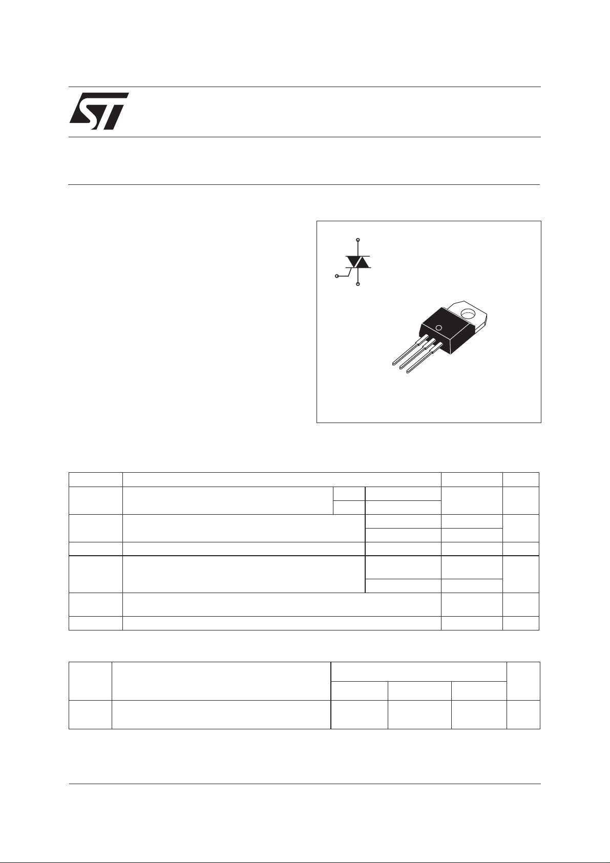
BTB04 T/D/S/A
SENSITIVE GATE TRIACS
A2
G
A1
A1
A2
G
TO-220AB
ABSOLUTE RATINGS (limiting values)
Symbol Parameter Value Unit
I
T(RMS)
I
TSM
2
I
dI/dt Critical rate of rise of on-state current
Tstg
Tj
Tl Maximum lead soldering temperature during 10s at 4.5mm from case 260 °C
Symbol Parameter
V
DRM
V
RRM
RMS on-state current (360° conduction angle) BTA Tc = 90°C 4 A
BTB Tc = 95°C
Non repetitive surge peak on-state current
(Tj initial = 25°C)
tI
2
t value tp = 10ms 8 A2s
Gate supply: I
Storage and operating junction temperature range -40 to +150
= 50mA dIG/dt = 0.1A/µs
G
400 T/D/S/A 600 T/D/S/A 700 T/D/S/A
Repetitive peak off-state voltage Tj = 110°C
tp = 8.3ms 42 A
tp = 10ms 40
Repetitive
F = 50Hz
Non repetitive 50
-40 to +110
BTA / BTB04-
400 600 700 V
10 A/µs
°C
Unit
September 2001 - Ed: 1A
1/6
BTA04 T/D/S/A BTB04 T/D/S/A
THERMAL RESISTANCE
Symbol Parameter Value Unit
Rth (j-a) Junction to ambient 60 °C/W
Rth (j-c) DC JunctiontocaseforDC BTA 4.4 °C/W
BTB 3.2
Rth (j-c) AC Junction to case for 360° conduction angle (F = 50Hz) BTA 3.3 °C/W
BTB 2.4
GATE CHARACTERISTICS (maximum values)
P
ELECTRICAL CHARACTERISTICS
=1W PGM= 40W (tp = 20µs) IGM= 4A (tp = 20µs) VGM= 16V (tp = 20µs)
G(AV)
Symbol Test conditions Quadrant
BTA / BTB04
TDSA
I
GT
VD= 12V (DC) RL=33Ω Tj = 25°C I - II - III MAX. 5 5 10 10 mA
IV MAX. 5 10 10 25
V
GT
V
GD
tgt VD=V
I
VD= 12V (DC) RL=33Ω Tj = 25°C I - II - III - IV MAX. 1.5 V
VD=V
DRM
DRMIG
dI
/dt = 0.5A/µs
G
IG= 1.2I
L
GT
RL= 3.3kΩ Tj =110°C I - II - III - IV MIN. 0.2 V
= 40mA
Tj = 25°C I - II-III-IV TYP. 2 µs
Tj = 25°C I - III - IV TYP. 10 10 20 20 mA
II 20 20 40 40
*I
I
H
= 100mA Gate open Tj = 25°C MAX. 15 15 25 25 mA
T
VTM*ITM= 5.5A tp = 380µs Tj = 25°C MAX. 1.65 V
I
DRM
I
RRM
V
V
DRM
RRM
rated
rated
Tj = 25°C MAX. 0.01 mA
Tj = 110°C MAX. 0.75
dV/dt * Linearslopeupto
VD= 67% V
DRM
gate open
Tj = 110°C TYP. 10 10 - - V/µs
MIN. - - 10 10
Unit
(dI/dt)c* (dI/dt)c = 1.8A/ms Tj = 110°C TYP. 1 1 5 5 V/µs
* For either polarity of electrode A2voltage with reference to electrode A
1
2/6

PRODUCT INFORMATION
BTA04 T/D/S/A BTB04 T/D/S/A
I
Package
BTA
(Insulated)
BTB
(Uninsulated)
ORDERING INFORMATION
T(RMS)
A V TDSA
4 400 X X
Triac
Series
Insulation:
A: insulated
B: non insulated
Current: 04A
V
DRM/VRRM
600 X X
700 X X
400 X X
600 X X
Sensitivity Specification
BT A 04 - 400 T
Sensitivity
Voltage:
400: 400V
600: 600V
700: 700V
3/6

BTA04 T/D/S/A BTB04 T/D/S/A
Fig. 1: Maximum RMS power dissipation versus
RMS on-state current (F = 50Hz).(Curves are cut
off by (dI/dt)c limitation)
Fig. 3: Correlation between maximum RMS power
dissipation and maximum allowable temperature
(TambandTcase)for different thermalresistances
heatsink + contact (BTB).
Fig. 2: Correlation between maximum RMS power
dissipation and maximum allowable temperature
(Tamb and Tcase) for different thermal resistances
heatsink + contact (BTA).
Fig. 4: RMS on-state current versus case temperature.
Fig. 5: Relative variation of thermal impedance
versus pulse duration.
Zth/Rth
1
Zth(j-c)
0.1
0.01
1E-3 1E-2 1E-1 1E+0 1E+1 1E+2 5E+2
4/6
Zth(j-a)
tp(s)
Fig. 6: Relative variation of gate trigger current
and holding current versus junction temperature.

BTA04 T/D/S/A BTB04 T/D/S/A
Fig. 7: Non repetitive surge peak on-state current
versus number of cycles.
Fig. 9: On-state characteristics (maximum values).
Fig. 8: Non repetitive surge peak on-state current
forasinusoidalpulsewithwidth: t ≤ 10ms, and corresponding value of I
2
t.
5/6

BTA04 T/D/S/A BTB04 T/D/S/A
PACKAGE MECHANICAL DATA
TO-220AB (Plastic)
B
b2
L
I
A
l4
a1
l3
l2
a2
b1
e
DIMENSIONS
REF.
C
Millimeters Inches
Min. Typ. Max. Min. Typ. Max.
A 15.20 15.90 0.598 0.625
a1 3.75 0.147
F
a2 13.00 14.00 0.511 0.551
B 10.00 10.40 0.393 0.409
b1 0.61 0.88 0.024 0.034
b2 1.23 1.32 0.048 0.051
C 4.40 4.60 0.173 0.181
c1 0.49 0.70 0.019 0.027
c2
c2 2.40 2.72 0.094 0.107
e 2.40 2.70 0.094 0.106
F 6.20 6.60 0.244 0.259
I 3.75 3.85 0.147 0.151
I4 15.80 16.40 16.80 0.622 0.646 0.661
M
c1
L 2.65 2.95 0.104 0.116
l2 1.14 1.70 0.044 0.066
l3 1.14 1.70 0.044 0.066
M 2.60 0.102
OTHER INFORMATION
Ordering type Marking Package Weight Base qty Delivery mode
BTA/BTB04-xxxy BTA/BTB04-xxxy TO-220AB 2.3 g 250 Bulk
■
Epoxy meets UL94,V0
■
Cooling method: C
■
Recommended torque value: 0.8 m.N.
■
Maximum torque value: 1 m.N.
Informationfurnished isbelieved tobe accurateand reliable.However, STMicroelectronics assumesno responsibilityfor theconsequences of
useof suchinformation norfor anyinfringement ofpatents orother rightsof thirdparties whichmayresult fromits use.No licenseis grantedby
implication or otherwise under any patent or patent rights of STMicroelectronics. Specifications mentioned in this publication are subject to
change withoutnotice. This publication supersedesand replaces all informationpreviously supplied.
STMicroelectronics products are not authorized for use as critical componentsin life support devices or systemswithout express written approval ofSTMicroelectronics.
The ST logo is a registered trademark of STMicroelectronics
© 2001 STMicroelectronics - Printed in Italy - All rights reserved.
STMicroelectronics GROUP OF COMPANIES
Australia - Brazil - China - Finland - France - Germany - Hong Kong - India - Italy - Japan - Malaysia
Malta - Morocco - Singapore - Spain - Sweden - Switzerland - United Kingdom - U.S.A.
http://www.st.com
6/6
 Loading...