


BD707/709/711
BD708/712
COMPLEMENTARY SILICON POWER TRANSISTORS
■ COMPLEMENTARYPNP- NPNDEVICES
APPLICATION
■ LINEARAND SWITCHING INDUSTRIAL
EQUIPMENT
DESCRIPTION
The BD707, BD709 and BD711 are silicon
Epitaxial-Base NPN power transistors in Jedec
TO-220 plastic package. They are intented for
usein powerlinearand switching applications.
The BD707 and BD711 complementary PNP
types are BD708 and BD712 respectively.
TO-220
3
2
1
INTERNAL SCHEMATIC DIAGRAM
ABSOLUTE MAXIMUM RATINGS
Symbol Parameter Value Unit
NPN BD707 BD70 9 BD711
PNP BD708 BD71 2
V
V
V
V
I
P
T
For PNP types voltage and current values are negative
Coll ect o r -B a s e V o lt age (IE=0) 60 80 100 V
CBO
Coll ect o r -E mitter Volt a ge (VBE=0) 60 80 100 V
CER
Coll ect o r -E mitter Volt a ge (IB=0) 60 80 100 V
CEO
Emit ter-B ase Voltage (IC=0) 5 V
EBO
I
Coll ect o r Curr e nt 12 A
C
Coll ect o r Peak Cu rr ent 18 A
CM
I
Base Current 5 A
B
Total Dissipation a t Tc≤ 25oC
tot
St orage Te mperat ur e -65 t o 15 0
stg
T
Max. Operating Junction Temperature 150
j
75 W
o
C
o
C
September 1999
1/6

BD707/708/709/711/712
THERMAL DATA
R
thj-case
R
thj-case
Ther mal Resistan c e Juncti on-cas e Max
Ther mal Resistan c e Juncti on-ambient Max
1.67
70
o
C/W
o
C/W
ELECTRICAL CHARACTERISTICS
=25oC unless otherwisespecified)
(T
case
Symbol Parameter Test Conditions Min. Typ. Max. Unit
I
CBO
I
CEO
I
EBO
V
CEO(sus )
V
CE(sat)
Collec to r Cut-of f
Current (I
E
=0)
Collec to r Cut-of f
Current (I
B
=0)
Emitter Cut-off Current
=0)
(I
C
∗ Collector-E mitte r
Sust aining Volta ge
=0)
(I
B
∗ Collector-Emitte r
for BD707/ 708 V
for BD709 V
for BD711/ 712 V
=150oC
T
case
for BD707/ 708 V
for BD709 V
for BD711/ 712 V
for BD707/ 708 V
BD709
for
for BD711/ 712 V
V
=5V 1 mA
EB
I
=100mA
C
for BD707/ 708
for BD709
for BD711/712
CB
CB
CB
CB
CB
CB
CE
V
CE
CE
=60V
=80V
= 100 V
=60V
=80V
= 100 V
=30V
=40V
=50V
60
80
100
IC=4A IB=0.4A 1 V
100
100
100
1
1
1
100
100
100
Sat uration V oltage
V
CEK
V
BE
h
FE
f
∗
Pulsed: Pulse duration = 300 µs, duty cycle 1.5 %
** Valuefor which I
For PNP types voltage and current values are negative.
Knee Voltage I
∗
=3A IB=** 0.4 V
C
∗ Base-Emitter Voltage IC=4A VCE=4V 1.5 V
DC Curre nt Gain I
∗
Tr ansition fr equ ency IC=300mA VCE=3V 3 MHz
T
=3.3 A at VCE= 2V.
C
=0.5A VCE=2V
C
=2A VCE=2V
I
C
for BD707/70 8
for
=4A VCE=4V
I
C
=10A VCE=4V
I
C
for BD707/70 8
BD709
for
for BD711/ 712
BD709
40
30
30
15
120
400
150
5
10
8
8
µA
µ
µA
mA
mA
mA
mA
mA
mA
V
V
V
A
2/6

BD707/708/709/711/712
SafeOperating Areas
DC Current Gain(NPN type)
DeratingCurve
DC Current Gain(PNP type)
DC Transconductance(NPNtype)
DC Transconductance(PNPtype)
3/6

BD707/708/709/711/712
Collector-EmitterSaturationVoltage (NPN type) Collector-EmitterSaturationVoltage (PNP type)
Base-EmitterSaturationVoltage (NPN type) Base-EmitterSaturation Voltage (PNP type)
TransitionFrequency(NPN type) TransitionFrequency(PNP type)
4/6
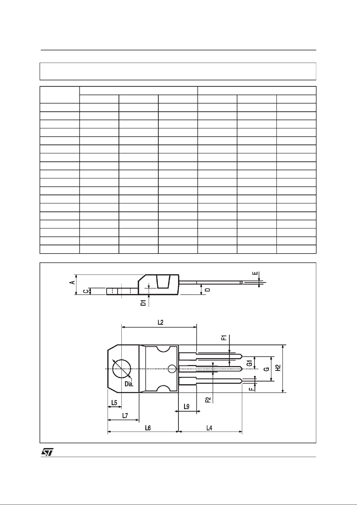
TO-220 MECHANICAL DATA
BD707/708/709/711/712
DIM.
MIN. TYP. MAX. MIN. TYP. MAX.
A 4.40 4.60 0.173 0.181
C 1.23 1.32 0.048 0.051
D 2.40 2.72 0.094 0.107
D1 1.27 0.050
E 0.49 0.70 0.019 0.027
F 0.61 0.88 0.024 0.034
F1 1.14 1.70 0.044 0.067
F2 1.14 1.70 0.044 0.067
G 4.95 5.15 0.194 0.203
G1 2.4 2.7 0.094 0.106
H2 10.0 10.40 0.393 0.409
L2 16.4 0.645
L4 13.0 14.0 0.511 0.551
L5 2.65 2.95 0.104 0.116
L6 15.25 15.75 0.600 0.620
L7 6.2 6.6 0.244 0.260
L9 3.5 3.93 0.137 0.154
DIA. 3.75 3.85 0.147 0.151
mm inch
P011C
5/6

BD707/708/709/711/712
Information furnished is believed to be accurate and reliable. However, STMicroelectronics assumes no responsibility for the consequences
of use of such information nor for any infringement of patents or other rights of third parties which may result from its use. No license is
granted by implication or otherwise under any patent or patentrights of STMicroelectronics. Specification mentioned in this publication are
subject to change without notice. This publication supersedes and replaces all information previously supplied. STMicroelectronics products
are not authorized for use as critical components inlife support devices or systems without express written approval of STMicroelectronics.
The ST logo is a trademarkof STMicroelectronics
1999 STMicroelectronics – Printed in Italy – All Rights Reserved
STMicroelectronics GROUP OF COMPANIES
Australia - Brazil -China - Finland - France- Germany - Hong Kong - India - Italy - Japan - Malaysia - Malta - Morocco -
Singapore - Spain - Sweden -Switzerland - United Kingdom - U.S.A.
http://www.st.com
.
6/6
 Loading...