

SGS Thomson Microelectronics BD682, BD681, BD680A, BD678A, BD678 Datasheet
...
POWER DARLINGTON TRANSISTORS
■ SGS-THOMSONPREFERRED SALESTYPES
■ COMPLEMENTARYPNP - NPN DEVICES
■ MONOLITHICDARLINGTON
CONFIGURATION
■ INTEGRATED ANTIPARALLEL
COLLECTOR-EMITTERDIODE
APPLICATION
■ LINEARAND SWITCHING INDUSTRIAL
EQUIPMENT
BD677/A/679/A/681
BD678/A/680/A/682
COMPLEMENTARY SILICON
1
2
3
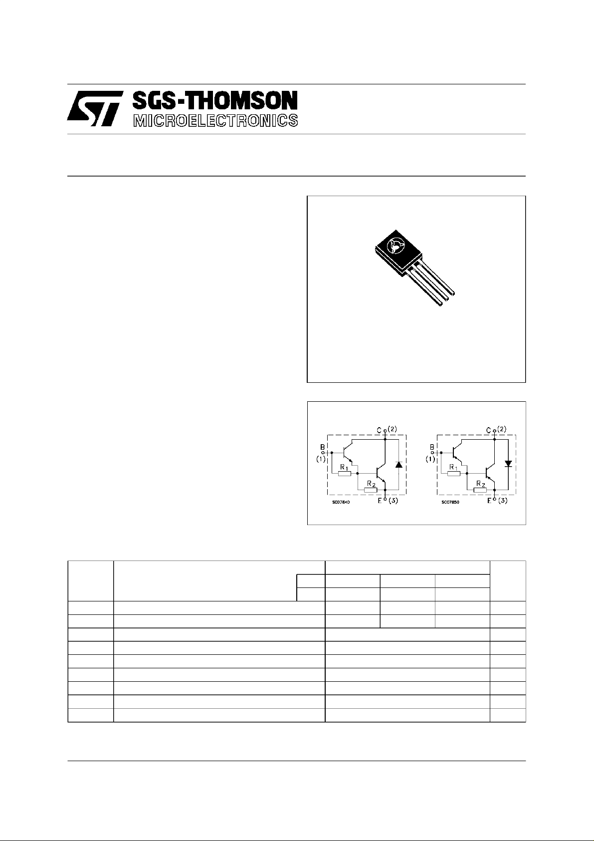
DESCRIPTION
SOT-32
The BD677, BD677A, BD679, BD679A and
BD681 are silicon epitaxial-base NPN power
transistors in monolithic Darlington configuration
mounted in Jedec SOT-32 plastic package.
They are intended for use in medium power linar
and switching applications
INTERNAL SCHEMATIC DIAGRAM
The complementary PNP types are BD678,
BD678A, BD680, BD680A and BD682
respectively.
R1Typ.= 7 K Ω R2Typ.= 230 Ω
ABSOLUTE MAXIMUM RATINGS
Symbol Parameter Value Unit
NPN BD677/A BD679/A BD681
PNP BD678/ A BD680/A BD682
V
V
V
I
P
T
For PNP types voltage and current values are negative.
Collect or- B as e V o lt age (IE=0) 60 80 100 V
CBO
Collector-Emitter Voltage (IB=0) 60 80 100 V
CEO
Emitter-Base Voltage ( IC=0) 5 V
EBO
Collect or Cur rent 4 A
I
C
Collect or P ea k Current 6 A
CM
Base Current 0.1 A
I
B
Tot al Dissipation at Tc≤ 25oC40W
tot
Storage Temperature -65 to 1 50
stg
Max. Operating Junc t i on Temperat ure 150
T
j
o
C
o
C
September 1997
1/6
BD677/677A/678/678A/679/679A/680/680A/681/682
THERMAL DATA
R
thj-case
R
thj-amb
Ther mal Resistance Junct io n-c ase Max
Ther mal Resistance Junct io n-am bien t Max
3.12
100
o
C/W
o
C/W
ELECTRICAL CHARACTERISTICS (T
=25oC unlessotherwise specified)
case
Symbol Parameter Test Cond ition s Min. Typ. Max. Unit
I
CBO
I
CEO
I
EBO
V
CEO(sus )
V
CE(sat)
Collector Cut -off
Current (I
E
=0)
Collector Cut -off
Current (I
B
=0)
Emit ter Cut - o f f Curr ent
=0)
(I
C
Collector-E m it t er
Sust aining Voltage
∗
Collector-E m it t er
Saturation Voltage
∗
=ratedV
V
CE
VCE=ratedV
V
= half rated V
CE
V
=5V
EB
I
=50mA
C
CBO
CBO
TC= 100oC
CEO
for B D677 / 677A/678/678A
for B D679 / 679A/680/680A
for B D681 / 682
for B D677 / 678/679/ 6 80/ 681 / 682
I
=1.5A IB=30mA
C
for B D677 A/678A/ 6 79A/ 6 80A
=2A IB=40mA
I
C
0.2
2
0.5 mA
2mA
60
80
100
2.5
2.8
Base-Emitt er V oltage fo r BD677/ 678/679/ 6 80/ 681 / 682
=1.5A VCE=3V
I
V
∗
BE
C
for B D677 A/678A/ 6 79A/ 6 80A
=2A VCE=3V
I
C
2.5
2.5
DC C urr ent Gain for BD677 / 678/679/680/681 / 682
h
∗
FE
h
∗
Pulsed: Pulse duration = 300 µs, duty cycle 1.5 %
Small Signal Curr ent
fe
Gain
I
=1.5A VCE=3V
C
for B D677 A/678A/ 6 79A/ 6 80A
=2A VCE=3V
I
C
IC=1.5A VCE=3V f=1MHz
750
750
1
mA
mA
V
V
V
V
V
V
V
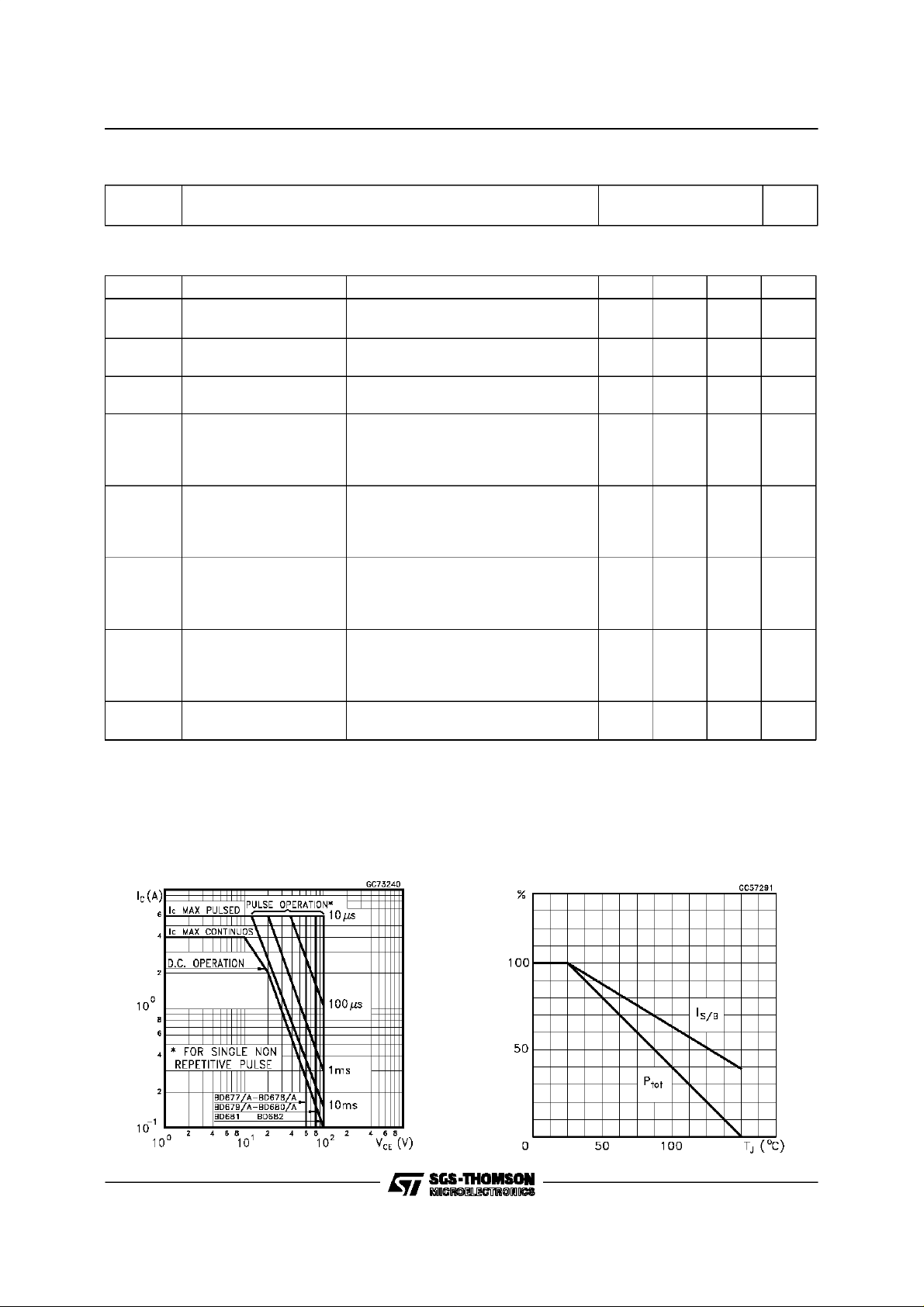
Safe Operating Areas DeratingCurve
2/6
 Loading...