

Page 1
SERVICE MANUAL
FILE NO.
Digital Camera
AC adaptor
Contents
1. OUTLINE OF CIRCUIT DESCRIPTION .................... 2
2. DISASSEMBLY ........................................................ 11
3. ELECTRICAL ADJUSTMENT .................................. 13
4. USB STORAGE INFORMATION
REGISTRATION ...................................................... 18
5. TROUBLESHOOTING GUIDE................................. 19
6. PARTS LIST............................................................. 20
CABINET AND CHASSIS PARTS 1 ........................ 20
CABINET AND CHASSIS PARTS 2 ........................ 21
ELECTRICAL PARTS .............................................. 22
ACCESSORIES & PACKING MATERIALS ............. 26
AC Adaptor .............................................................. 26
CIRCUIT DIAGRAMS &
PRINTED WIRING BOARDS ...................................... C1
VPC-R1
(Product Code : 126 293 00)
(U.S.A., Canada)
VPC-R1E
(Product Code : 126 293 01)
(U.K.)
VPC-R1EX
(Product Code : 126 293 02)
(Europe, PAL General)
VPC-R1G
(Product Code : 126 293 06)
(No Tax)
VAR-G5U
(Product Code : 126 301 01)
(U.S.A., Canada)
VAR-G5EX
(Product Code : 126 301 02)
(Europe, PAL General)
VAR-G5E
(Product Code : 126 301 03)
(U.K.)
PRODUCT SAFETY NOTICE
The components designated by a symbol ( ! ) in this schematic diagram designates components whose value are of
special significance to product safety. Should any component designated by a symbol need to be replaced, use only the part
designated in the Parts List. Do not deviate from the resistance, wattage, and voltage ratings shown.
CAUTION : Danger of explosion if battery is incorrectly replaced.
Replace only with the same or equivalent type recommended by the manufacturer.
Discard used batteries according to the manufacturer’s instructions.
NOTE : 1. Parts order must contain model number, part number, and description.
2. Substitute parts may be supplied as the service parts.
3. N. S. P. : Not available as service parts.
Design and specification are subject to change without notice.
SB117/U, E, EX, EX2, SVA01/U, EX, E
REFERENCE No. SM5310265
Page 2
1. OUTLINE OF CIRCUIT DESCRIPTION
1-1. CA-A CIRCUIT DESCRIPTIONS
Around CCD block
1. IC Configuration
IC903 (RJ24J1AA0PT) CCD imager
IC902 (TC74VHC04FTP) H driver
IC904 (LR366854) V driver
IC905 (AD9806KST) CDS, AGC, A/D converter
PI4
PI3
(NC)
3 2 1 21
4
(NC)
(NC)
2324
(NC)
22
PI2
PI1
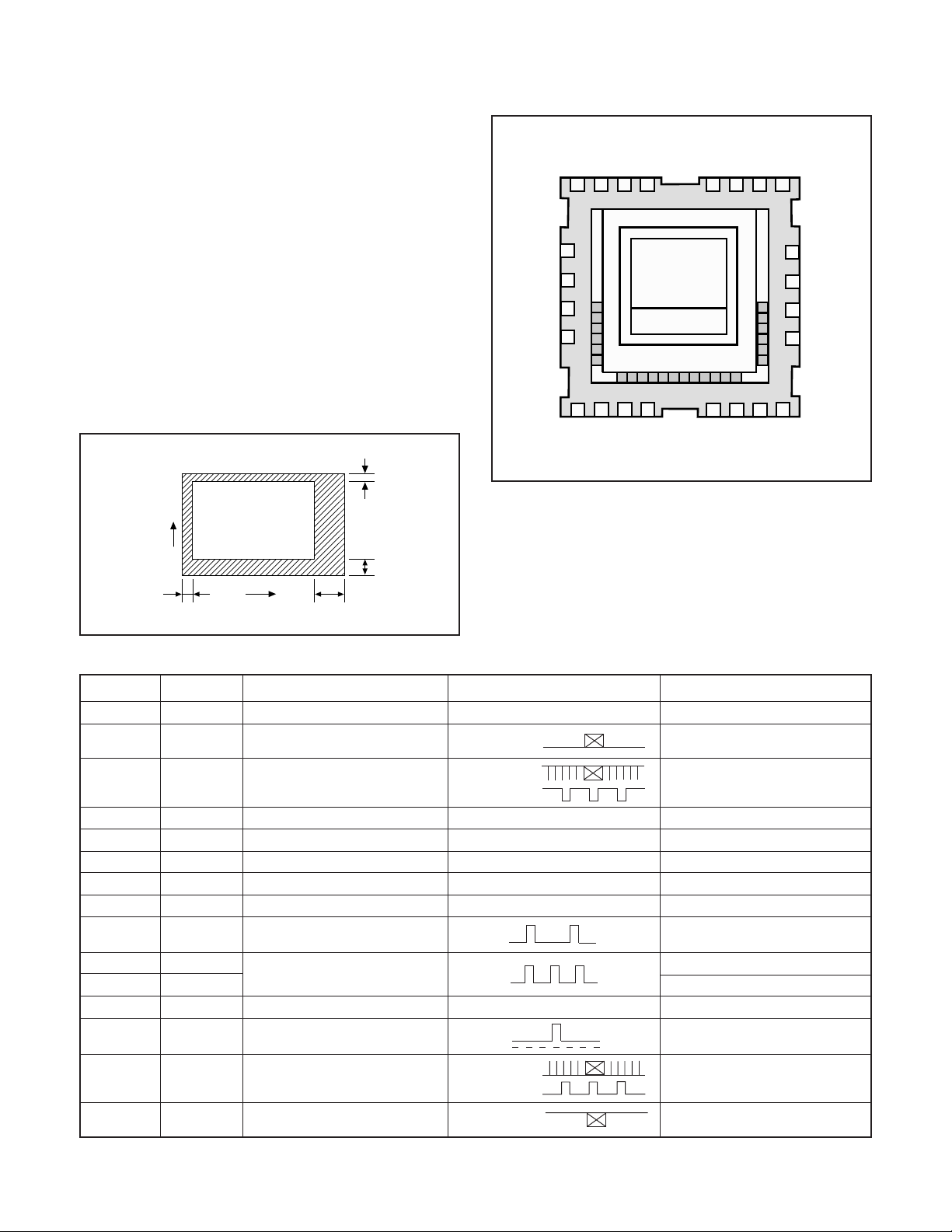
2. IC905 (CCD)
[Structure]
Frame transfer type CCD image sensor
Optical size 1/2.8 type
Effective pixels 1300 (H) x 980 (V)
Pixels in total 1353 (H) x 1006 (V)
Optical black
Horizontal (H) direction: left 2 pixels, right 51 pixels
Vertical (V) direction: upper 10 pixels, below 12 pixels
Dummy bit number Horizontal : 20 Vertical : 4
10
V
12
2
Fig. 1-1.Optical Black Location (Top View)
Pin No. Symbol
1, 2, 23, 24
NC
H
Pin Description
-
51
PS1
5
PS2
6
7
VPW
8
VOUT
9
Waveform
(LCC24
Top View)
10
11 12 16
PR
VSS
VDD
VRD
PH4
151413
PH1
Fig. 1-2. CCD Terminal Name
Voltage
PH2
20
19
18
17
PH3
PS3
PS4
NSUB
VOG
3, 4
5, 6
7
8
9
10
11
12
13, 15
14, 16
17
18
19, 20
PI3, PI4
PS1, PS2
PW
VOUT
VDD
VSS GND
VRD
PR
PH4, PH2
PH1, PH3
VOG
VSUB
PS4, PS3
21, 22 PI1, PI2
Image clock
Accumulation clock
P well
CCD output
Power
Reset drain
Reset gate
Horizontal register clock
CCD output gate
N substrate
Accumulation clock
Image clock
Table 1-1. CCD Pin Description
Frame shift
Frame shift
Line sending
Frame shift
Line sending
Frame shift
DC
DC
DC
DC
DC
DC
0~12 V
0~12 V
8 V
Approx. 13 V
20 V
0 V
20 V
L=18 V, H=23 V
L=2.5 V, H=7.5 V
L=0 V, H=5 V
3.3 V
L=26 V, H=29 V
0~12 V
0~12 V
– 2 –
Page 3
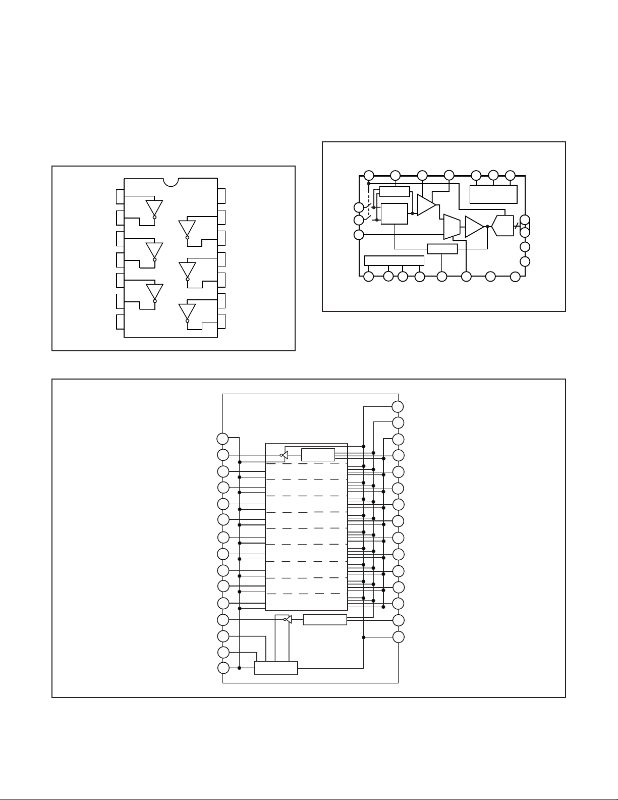
3. IC903 (H Driver) and IC902 (V Driver)
An H driver (IC903) and V driver (IC902) are necessary in
order to generate the clocks (vertical transfer clock, horizontal transfer clock and electronic shutter clock) which driver
the CCD.
IC902 is an inverter IC which drives the horizontal CCDs (H1
and H2). In addition the VREG 0~7, VXREG2 and VXREG3
signals which are output from IC102 are the vertical transfer
clocks. The clock is drived until peak value which necessary
CCD at IC902.
14
CC
1A
1Y
2A
2Y
3A
3Y
GND
1
2
3
4
5
6
7
V
13
6A
12
6Y
11
5A
10
5Y
4A
9
4Y
8
4. IC901 (CDS, AGC Circuit and A/D Converter)
The video signal which is output from the CCD is input to
Pins (26) and (27) of IC901. There are S/H blocks inside IC905
generated from the XSHP and XSHD pulses, and it is here
that CDS (correlated double sampling) is carried out.
After passing through the CDS circuit, the signal passes
through the AGC amplifier. It is A/C converted internally into
a 10-bit signal, and is then input to IC102.
SHD ADCCLK
22
21
GENERATOR
16
TIMING
A/D
AD9802
3341
ACVDD
ADVDD
43
10
2
DOUT
11
DRVDD
12
DVDD
17
PIN
DIN
ADCIN
PBLK
CLPDM SHP
CLAMP
27
26
CDS
29
2319
PGA
36
CLAMP
REFERENCE
48
37 20
CMLEVEL
VRT
47
VTB
STBY CLPOB
18
Fig. 1-5. IC901 Block Diagram
30
MUX S/H
ADCMODE
Fig. 1-3. IC903 Block Diagram
GND
1
OUT_1
2
OUT_2
3
OUT_3
4
OUT_4
5
OUT_5
6
OUT_6
7
OUT_7
8
OUT_8
9
OUT_9
10
OUT_10
OUT_NSUB
CAP5V
CAPNS
GND
11
12
13
14
15
Power circuit
OCNT circuit
DUTY circuit
OCNT circuit
30
29
28
27
26
25
24
23
22
21
20
19
18
17
16
VDD
OCNT
DUTY
IN_1
IN_2
IN_3
IN_4
IN_5
IN_6
IN_7
IN_8
IN_9
IN_10
IN_NSUB
VDD
Fig. 1-4. IC902 Block Diagram
– 3 –
Page 4
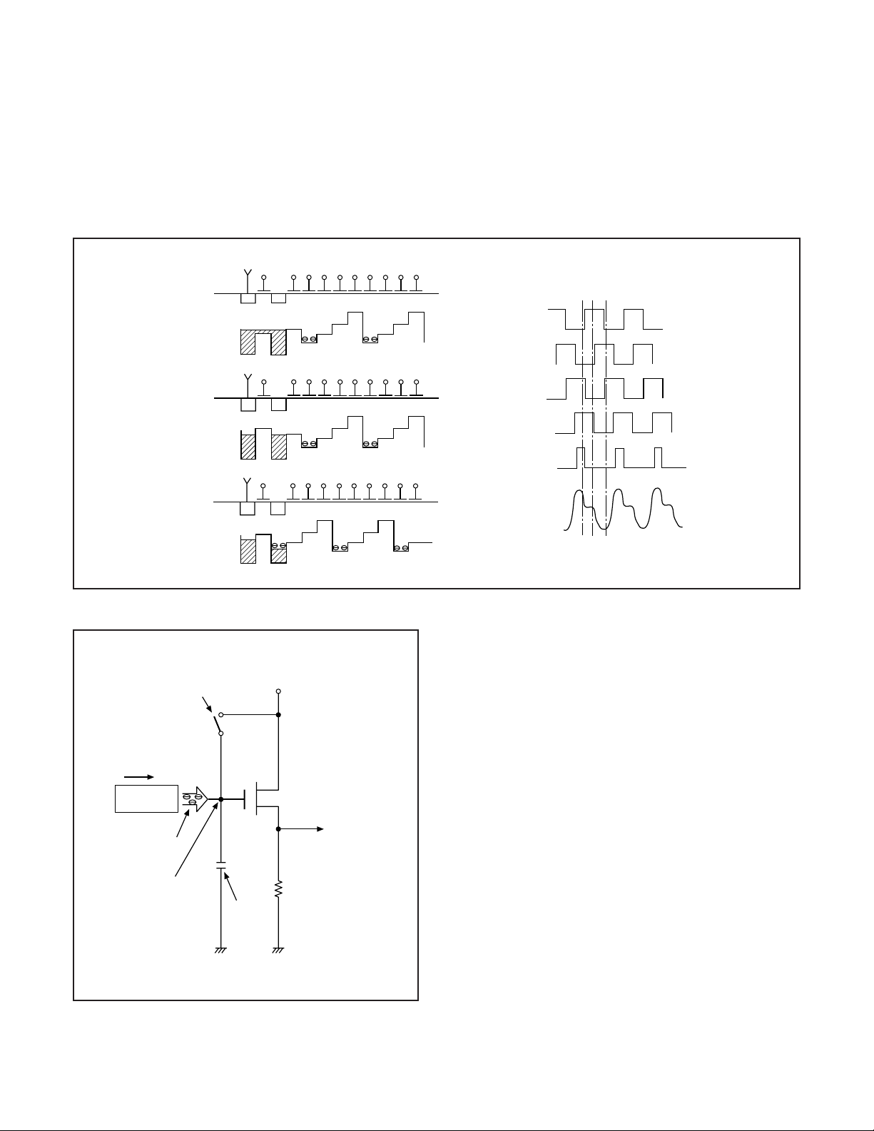
5. Transfer of Electric Charge by the Horizontal CCD
The transfer system for the horizontal CCD emplays a 4-phase drive method.
The electric charges sent to the final stage of the horizontal CCD are transferred to the floating diffusion (FD), as shown in Fig.
1-6. PR is turned on by the timing in (1), and the floating diffusion is charged to the potential of RD.
The PR is turned off by the timing in (2). In this condition, the floating diffusion is floated at high impedance.
The H2 potential becomes shallow by the timing in (3), and the electric charge now moves to the floating diffusion.
Here, the electric charges are converted into voltages at the rate of V = Q/C by the equivalent capacitance C of the floating
diffusion. PR is then turned on again by the timing in (1) when the H2 potential becomes deep.
Thus, the potential of the floating diffusion changes in proportion to the quantity of transferred electric charge, and becomes
CCD output after being received by the source follower. The equivalent circuit for the output circuit is shown in Fig. 1-7.
Reset gate pulse
Direction of transfer
(1)
(2)
(3)
PR
PR
PR
OG
H2
H1 H4 H3 H2 H1 H4 H3
(1)(2)
FDRD
H3
H4
OG
H2
H1 H4 H3 H2 H1 H4 H3
H1
FDRD
H2
PR
OG
H2
H1 H4 H3 H2 H1 H4 H3
FDRD
CCD OUT
(3)
Fig. 1-6. Horizontal Transfer of CCD Imager and Extraction of Signal Voltage
6. Lens drive block
6-1. Shutter drive
The regulator (IC952) drives by P ON signal which is output
20 V Pre-charge drain bias (PD)
from the power control IC (IC501) is drived, and then power is
supplied to iris shutter drive IC (IC951). The drive signal
(GPIO4, GPIO5, GPIO6, GPIO7) which is output from the
ASIC (IC102) is drived the iris shutter drive IC (IC951), and
the iris shutter spring is open and closed.
H Register
Electric
charge
Floating diffusion gate is
floated at a high impedance.
C is charged
equivalently
Voltage output
Fig. 1-7. Theory of Signal Extraction Operation
– 4 –
Page 5

1-2. CA-B CIRCUIT DESCRIPTION
1. Circuit description
1-1. PTG
This is program timing generator. Generates the timing signal
that is needed in order to drive the FT-CCD sensor.
1-2. FCP
The FCP receives the output data from the FT-CCD sensor
via the PTG, and then carries out various processing operations on the data (such as gamma correction and white
banance).
1-3. ITP
The ITP is a pixel conversion processor. It carries out various
processing operations (such as contour emphasis and chroma)
on the image data that is input from the FCP or from memory,
and then stores the processed data in memory.
1-4. CPU
This is 32 bit RISC CPU.
1-5. Memory controller
This is controlled SDRAM, flash ROM and CF card etc.
1-6. Video player
Outputs the RGB signals that are needed to control the graphic
overlay function and to drive the LCD.
1-7. GPIO
This is a multipurpose I/O. (It can be used as an input/output
port.)
1-8. COM port
This is communication block. Supports USB communication.
2. Outline of Operation
When the shutter opens, detect the 8-bit microprocessor and
transmit to record operation starts.
When the PTG drives the FT-CCD, picture data passes
through the A/D and is then input to the ASIC as 10-bit data.
This data then sends FCP, after which it is carried out various
processing operations on the data (such as gamma correction and white balance). The data is then sent to the ITP where
processing such as contour emphasis and chroma are carried out, after which it is temporarily stored in the SDRAM.
In case of still picture the data is then compressed by the
JPEG method and in case of picture it is compressed by
MJPEG method and is written to compact flash card.
3. LCD Block
RGB signals corresponding to the LCD driver are output from
the ASIC (video player). The LCD driver converts the RGB
signals that are output from the ASIC to a signal level that is
appropriate for the LCD monitor. These RGB signals and the
control signal which is output by the LCD driver are used to
drive the LCD panel.
The RGB signals are 1H transposed so that no DC component is present in the LCD element, and the two horizontal
shift register clocks drive the horizontal shift registers inside
the LCD panel so that the 1H transposed RGB signals are
applied to the LCD panel.
Because the LCD closes more as the difference in potential
between the VCOM (common polar voltage: fixed at DC) and
the R, G and B signals becomes greater, the display becomes
darker; if the difference in potential is smaller, the element
opens and the LCD become brighter. In addition, the brightness and contrast settings for the LCD can be varied by means
of the serial data from the ASIC.
1-9. Serial communication
This is the interface for the 8-bit microprocessor.
1-10. LCD driver
The RGB output signals that are output from the ASIC are
converted to a signal level that is appropriate for the LCD monitor.
1-11. LCD monitor
This is the image display device which displays the image
signals supplied from the LCD driver.
– 5 –
Page 6

1-3. CP1 POWER CIRCUIT DESCRIPTION
1. Outline
This is the main power circuit, and is comprised of the following blocks.
Switching controller (IC501)
Digital 5 V and analog system power output (T5001, Q5001)
Digital 2.5 V system power supply (Q5007)
Digital 3.4 V system power supply (Q5018)
LCD system power supply (Q5008, T5002)
Backlight power supply output (Q5013)
Inverter output (T5003, Q5017)
2. Switching Controller (IC501)
This is the basic circuit which is necessary for controlling the
power supply for a PWM-type switching regulator, and is provided with five built-in channels, only CH2 (digital 5 V, analog
system), CH4 (LCD system), CH3 (digital 2.5 V), CH1 (digital
3.4 V) and CH5 (backlight system) are used. Feedback from
5 V (D) (CH2), 2.5 V (D) (CH3) , 12.4 V (L) (CH4), 3.4 V (D)
(CH1) and 7 V (L) (CH5) power supply outputs are received,
and the PWM duty is varied so that each one is maintained at
the correct voltage setting level.
2-1. Short-circuit protection circuit
If output is short-circuited for the length of time determined
by the condenser which is connected to Pin (29) of IC501, all
output is turned off. The control signal (P ON) are recontrolled
to restore output.
3. Digital 3.4 V Power Output
3.4 V (D) is output. Feedback is sent to pin (41) of the switching controller (IC501) for PWM control to be carried out.
4. Digital 5 V and Analog System Power Output
5.1 V (D) , 26.4 V (A), 20 V (A), 13 V (A) and 5.1 V (A) are
output. Feedback for the 5.1 V (D) is provided to the switching controller (Pins (35) of IC501) so that PWM control can
be carried out.
5. Digital 2.5 V System Power Output
2.5 V (D) is output. Feedback is provided to the swiching controller (Pin (23) of IC501) so that PWM control can be carried
out.
6. LCD System Power Output
12.4 V (L) is output. Feedback for the 12.4 V (L) is provided
to the switching controller (Pins (22) of IC501) so that PWM
control can be carried out.
7. Backlight Power Supply output
7.0 V (L) is output. Feedback is sent to pin (17) of the switching controller (IC501) for PWM control to be carried out.
8. Inverter Output
The backlight uses a flat picture tube. When INV CLK is input, Q5017 carries out switching operations, so that T5003 is
energized and a high-voltage pulse is generated between pins
(3) and (4) of T5003. This high-voltage pulse is applied to the
backlight to make it illuminate.
– 6 –
Page 7

1-4. CP1 STROBO CIRCUIT DESCRIPTION
1. Charging Circuit
When UNREG power is supplied to the charge circuit and the
CHG signal becomes High (3.3 V), the charging circuit starts
operating and the main electorolytic capacitor is charged with
high-voltage direct current.
However, when the CHG signal is Low (0 V), the charging
circuit does not operate.
1-1. Power switch
When the CHG signal switches to Hi, Q5406 turns ON and
the charging circuit starts operating.
1-2. Power supply filter
L5401 and C5405 constitute the power supply filter. They
smooth out ripples in the current which accompany the switching of the oscillation transformer.
1-3. Oscillation circuit
This circuit generates an AC voltage (pulse) in order to increase the UNREG power supply voltage when drops in current occur. This circuit generates a drive pulse with a frequency
of approximately 50-100 kHz. Because self-excited light omission is used, the oscillation frequency changes according to
the drive conditions.
2. Light Emission Circuit
When RDY and TRIG signals are input from the ASIC, the
stroboscope emits light.
2-1. Emission control circuit
When the RDY signal is input to the emission control circuit,
Q5409 switches on and preparation is made to let current
flow to the light emitting element. Moreover, when a STOP
signal is input, the stroboscope stops emitting light.
2-2. Trigger circuit
When a TRIG signal is input to the trigger circuit, D5405
switches on, a high-voltage pulse of several kilovolts is generated inside the trigger circuit, and this pulse is then applied
to the light emitting part.
2-3. Light emitting element
When the high-voltage pulse form the trigger circuit is applied to the light emitting part, currnet flows to the light emitting element and light is emitted.
Beware of electric shocks.
1-4. Oscillation transformer
The low-voltage alternating current which is generated by the
oscillation control circuit is converted to a high-voltage alternating current by the oscillation transformer.
1-5. Rectifier circuit
The high-voltage alternating current which is generated at
the secondary side of T5401 is rectified to produce a highvoltage direct current and is accumulated at electrolytic capacitor C5412 on the main circuit board.
1-6. Voltage monitoring circuit
This circuit is used to maintain the voltage accumulated at
C5412 at a constance level.
After the charging voltage is divided and converted to a lower
voltage by R5417 and R5419, it is output to the SY-A block as
the monitoring voltage VMONIT. When this VMONIT voltage
reaches a specified level at the SY-A block, the CHG signal is
switched to Low and charging is interrupted.
– 7 –
Page 8

1-5. SY-A CIRCUIT DESCRIPTION
1. Configuration and Functions
For the overall configuration of the SY-A block, refer to the block diagram. The SY-A block centers around a 8-bit microprocessor
(IC301), and controls camera system condition (mode).
The 8-bit microprocessor handles the following functions.
1. Operation key input, 2. Clock control, 3. Power ON/OFF, 4. Strobe charge control.
Pin
1~2
3
4
5
6
7
8
9
10~12
13
14
15~16
17~18
19
20~23
24
25~26
27
28
29
30 SDIR
31 BAT_OFF
32 +3.2_SW
33
34 P ON
35~36
37
38
39~40
41
42
43
44~45
46
47
48~52
53
54~74
75~78
79~80
Signal
NOT USED
AVSS
AVR
AVCC
VDD3
UNREG (S)
VDD3
STROBO_V
P54~P56
VSS
DC_IN
X1, X0
MOD1, 0
P. ST.
S10~S13
P04
P05~P06
PLL_EN
USB_CNT
REQACK
RESET B
NOT USED
VF_LED_G
EXT_IRQ1
SDATA
SCLK
SELF_LED_R
NOT USED
X0A, X1A
BUZZER
CHARGE
NOT USED
VCC
NOT USED
SO0~SO3
NOT USED
I/O
O
O
O
O
O
O
O
I/O
O
O
O
O
O
Outline
-
-
-
-
I
I
I
I
I
-
I
-
I
I
I
I
I
I
I
I
-
-
-
-
-
-
-
-
GND
Analog power
Analog power
Main (ASIC system) power detection
Battery power input (analog input)
Main (ASIC system) power detection
Strobo charge voltage input (analog input)
Connect to GND through register
GND
AC adaptor connection detection (analog input)
Main clock oscillation terminal (4 MHz)
Connect to GND
Reset input
Key matrix input
Connect to GND through register
Connect to GND through register
ASIC PLL permission signal
USB connection detection H : Connection
Serial communication control signal
Serial communication control signal
Battery OFF detection H : OFF
3.2 V power (switch)
Reset output to ASIC L : Reset
DC/DC converter (analog) ON/OFF signal H : ON
-
VF LED (green) ON/OFF signal L : Light
External interruption signal
Serial communication control signal
Serial communication control signal
Self LED (red) ON/OFF signal L : Light
-
Sub clock oscillation terminal (32.768 kHz)
Buzzer output terminal
Strobo charge ON/OFF signal L : ON
-
Digital power
-
Key matrix output
-
Table 4-1. 8-bit Microprocessor Port Specification
– 8 –
Page 9
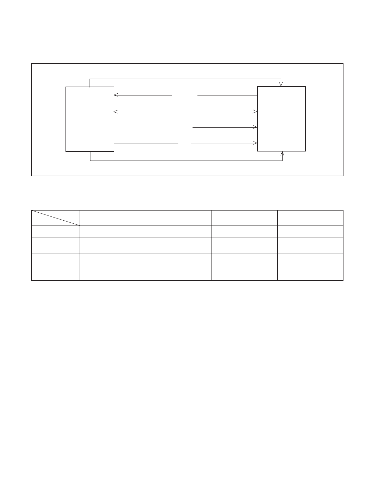
2. Internal Communication Bus
The SY-A block carries out overall control of camera operation by detecting the input from the keyboard and the condition of the
camera circuits. The 8-bit microprocessor reads the signals from each sensor element as input data and outputs this data to the
camera circuits (ASIC) or to the LCD display device as operation mode setting data. Fig. 4-1 shows the internal communication
between the 8-bit microprocessor, ASIC and SPARC lite circuits.
RESET B
REQACK
8-bit
Microprocessor
Fig. 4-1 Internal Bus Communication System
SDATA
SDIR
SCK
EXT_IRQ1
3. Key Operaiton
For details of the key operation, refer to the instruction manual.
SCAN
SCAN
OUT
IN
0
1
MAIN SW-PLAY POSITION
2
3
0
CF_IN
DOWN
-
1
TEST
MAIN SW-LCD OFF
POSITION
RIGHT
SET
Table 4-2. Key Operation
2
MAIN SW-LCD ON
POSITION
LEFT
MODE
ASIC
3
SHUTTER 1stSHUTTER 2nd
COVER SW
UP
FOCUS SW
– 9 –
Page 10
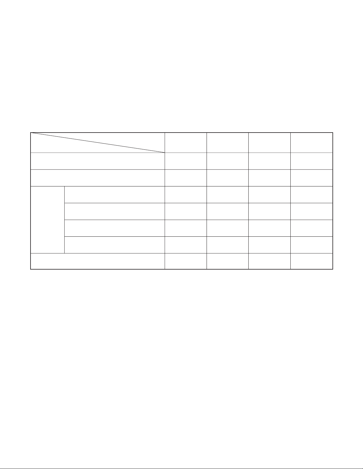
4. Power Supply Control
The 8-bit microprocessor controls the power supply for the overall system.
The following is a description of how the power supply is turned on and off. When the battery is attached, a regulated 3.2 V
voltage is normally input to the 8-bit microprocessor (IC301) by IC302, so that clock counting and key scanning is carried out
even when the power switch is turned off, so that the camera can start up again. When the battery is removed, the 8-bit microprocessor operates in sleep mode using the backup capacitor. At this time, the 8-bit microprocessor only carries out clock
counting, and waits in standby for the battery to be attached again. When a switch is operated, the 8-bit microprocessor supplies
power to the system as required.
The 8-bit microprocessor first sets the P ON signal at pin (34) to high, and then turns on the DC/DC converter for the digital
system. After this, it sets RESET B signal at pin (33) to high so that the ASIC is set to the active condition.
After this, in case of driving the CCD, it sets the P (A) ON signal at pin (176) of the ASIC to high, and then turns on the DC/DC
converter for the analog system.
If the LCD monitor is on, the LCD ON signal at pin (175) of the ASIC set to high, and the DC/DC converter for the LCD monitor
is turned on. Once it is completed, the ASIC returns to the reset condition, all DC/DC converters are turned off and the power
supply to the whole system is halted.
ASIC,
memory
Power voltage
Power OFF
Power switch ON-
Auto power OFF
Shutter switch ON
CAMERA
Resolution, flash, self-timer switch ON
LCD finder
Play back
Table 4-3. Camera Mode
Note) 4 MHz = Main clock operation, 32 kHz = Sub clock operation
3.3 V
OFF
OFF
ON
OFF
ON
ON
CCD
5 V (A)
+12 V etc.
OFF
OFF
→→
ON
→OFF
→→
OFF
ON
OFF
8 bit
CPU
3.2 V
(ALWAYS)
32KHz OFF
4 MHz OFF
4 MHz OFF
4 MHz OFF
4 MHz ON
4 MHz ON
MONITOR
+12 V etc.
LCD
– 10 –
Page 11
2. DISASSEMBLY
2-1. REMOVAL OF CABINET BACK, CABINET FRONT, TB1 BOARD AND LCD
1. Open the cover battery.
2. Four screws 1.7 x 4
3. Open the cover card.
4. Four screws 1.7 x 6
5. Cabinet back
6. Screw 1.7 x 4
7. Screw 1.7 x 6
8. Cabinet top A
9. Cabinet front
10. Cover battery
11. Cover card
12. Shaft card
5
12
11
3
9
6
F
2
7
8
D
4
E
H
4
C
B
A
2
The order of tighting screws
A→B→C→D→E→F→G→H
13. Screw 1.7 x 3.5
14. TB1 board
15. Spacer CV monitor 2
16. FPC
17. Remove the solder.
18. LCD
19. Three screws 1.7 x 4
20. Holder monitor
13
2
G
1
When assembling cabinet front
1. The cover lens should be closed.
2. Set the knob macro at the normal position.
10
brown
yellow
gray
18
15
19
14
20
pink
16
17
white
pink
white
– 11 –
Page 12
2-2. REMOVAL OF HOLDER CHASSIS, LENS ASSEMBLY, CP1 BOARD AND BOARD LOCATION
3
yellow
white
1
6
4
pink
gray
violet
1. Screw 1.7 x 3
2. Two screws 1.7 x 4
3. Holder chassis B
4. DL-elect
5. Screw 1.7 x 3
6. Switch leaf
7. Three screws 1.7 x 4
8. Two screws 1.7 x 5
9. FPC
10. CP1 board
2
TB1 board
blue
red
5
7
black
red
black
black
red
gray
10
black
red
8
CP1 board
– 12 –
9
Lens
CCD
Page 13
3. ELECTRICAL ADJUSTMENT
Firmware
Image
AWB
Focus
UV Matrix
R Bright
RGB Offset
Tint
B Bright
Gain
Phase
LCD
Calibration
Upload
Initialize
LCD Type
H AFC Test
VCOMDC
VCOMPP
Cal Data
Cal Mode
OK
OK
EVF
USB storage
Get
Set
VID
Set
PID
Set
Serial
Set
Rev.
Set
Setting
Language
Video Mode
VCO
Firmware Version:
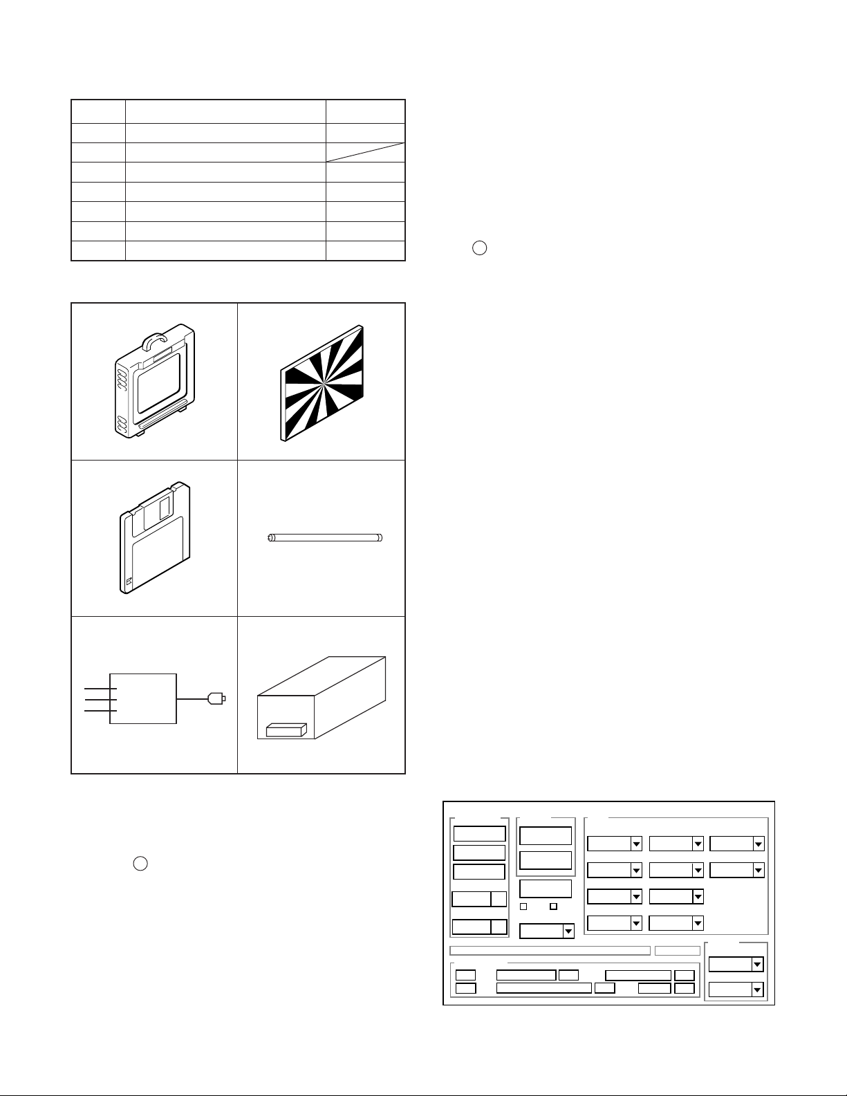
3-1. Table for Servicing Tools
Ref. No. Name
J-1
J-2
J-3
J-4
J-5
J-6
J-7
Note: J-1 color viewer is 100 - 110 VAC only.
J-1 J-2
J-3/J-7
Color viewer
Siemens star chart
Calibration software
Spare lamp
Pictured jig
Strobe adjustment box
CCD calibration
J-4
Part code
VJ8-0007
VJ8-0186
VJ8-0028
VJ8-0181
VJ8-0182
VJ8-0185
5. LCD Panel Adjustment
5-1. LCD H AFC Adjustment
5-2. LCD RGB Offset Adjustment
5-3. LCD Gain Adjustment
5-4. LCD Red Brightness Adjustment
5-5. LCD Blue Brightness Adjustment
3-4. Setup
1. System requirements
Windows 98 or Me
IBM R -compatible PC with pentium processor
CD-ROM drive
3.5-inch high-density diskette drive
USB port
40 MB RAM
Hard disk drive with at least 15 MB available
VGA or SVGA monitor with at least 256-color display
2. Installing calibration software
1. Insert the calibration software installation diskette into your
diskette drive.
2. Open the explorer.
3. Copy the DscCalDI_128a folder on the floppy disk in the
FD drive to a folder on the hard disk.
3. Installing USB drive
Install the USB drive with camera or connection kit for PC.
3-2. Equipment
1. Oscilloscope
2. Digital voltmeter
3. AC adaptor
4. PC (IBM R -compatible PC, Pentium processor, Window
5. Monitor TV
6. USB cable
3-3. Adjustment Items and Order
1. 5.1 V (A) Voltage Adjustment
2. Back Focus Adjustment
3. CCD Adjustment
4. Strobe Adjustment
J-5
98 or Me)
J-6
4. Color Viewer
1. Turn on the switch and wait for 30 minutes for aging to take
place before using Color Pure.
2. The luminance adjustment control on the color viewer
should be set to around the middle position (memory 5)
during use.
3. The fluorescent lamps which are used in the color viewer
are consumable parts. After the cumulative usage time
reaches 2000 hours, the color temperature will start to increase as the usage time increases, and correct adjustment will not be possible. When the cumulative usage time
reaches 2000 hours, all of the fluorescent lamps should be
simultaneously replaced with new lamps.
5. Computer screen during adjustment
– 13 –
Page 14
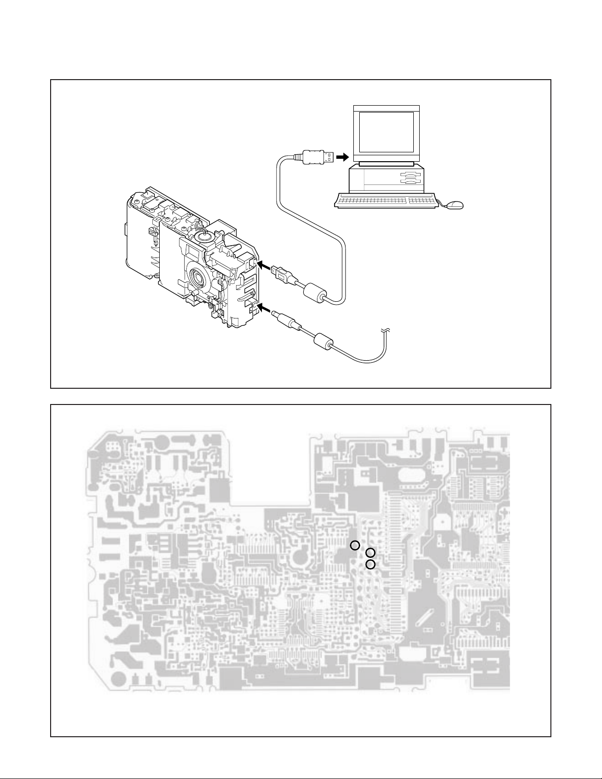
3-5. Connecting the camera to the computer and the pictured jig connection point
1. Line up the arrow on the cable connector with the notch on the camera's USB port. Insert the connector.
2. Locate a USB port on your computer.
To USB port
USB cable
GND
AC adaptor
VDD3
V OUT
Picutured jig connection point (CP1 board side B)
– 14 –
Page 15
3-6. Adjust Specifications
[CP1 board (Side B)]
CL307
CL528
VR502
(Side A)
Note:
1. Voltage adjustment is necessary to repair in the CP1 board
and replace the parts.
Preparation:
1. Shorten the CL307 and CL310 (connection parts of power
switch wires).
2. Insert the CF card.
3. Connect the power, and turn on the LCD monitor.
CL415
CL414
CL411
CL310
CL413
CL400
1. 5.1 V (A) Voltage Adjustment
6. Set the siemens star chart 130 cm +5 /–0 cm so that it becomes center of the screen.
7. Set the macro lever (2) at normal position.
8. Turn the adjustment screw (1) until the siemens is exactly
in focus. Focusing is done by moving from far focal length
to near focal length (conterclockwise motion of the dial), so
start adjustment by moving to the far focus position if the
camera in not already at that position.
9. Set the siemens star chart 25 cm + 3/–0 cm from the camera, check that the chart is out of focus this time.
10. Confirm that there are no operational problems in the com-
puter in taking still pictures in a set condition.
11. Pull the DC jack to turn off the camera after completing the
adjustment, and pull the CF card.
12. Remove the lead of the pictured jig. Confirm that there are
no operational problems in taking still pictures in a set
condition.
13. When this adjustment is carried out, it is necessary to per-
form the 3. CCD adjustment and 4. Strobe adjustment.
Perform the 4. Strobe adjustment after completing the
3. CCD adjustment.
3. CCD Adjustment
Measuring Point
Measuring Equipment
ADJ. Location
ADJ. Value
Adjustment method:
1. Adjust with VR502 to 5.10 ± 0.05 V.
CL528
Digital voltmeter
VR502
5.10 ± 0.05 V
2. Back Focus Adjustment
Adjustment
screw (1)
Macro
lever (2)
Normal position
Adjustment method:
1. Copy all the CCD calibration files to the CF card.
2. Click on Cmdfile.txt to activate the name field in the CF
card, and push the enter key to change the name to
“backfocus” using all lower case letters. Click the save button to save.
3. Take the lead of the pictured jig and solder it to the CP1
board, then connect the TV monitor. (Refer to page 14 below figure.)
4. Set the CF card which is saved to the camera.
5. Slide the lens cover and put DC jack to the camera in order
to turn on the camera.
Camera
18 cm
All white pattern
Color viewer
Adjustment method:
1. Copy all the CCD calibration files to the CF card.
2. Click on Cmdfile.txt to activate the name field in the CF
card, and push the enter key to change the name to “ccdcal”
using all lower case letters. Click the save button to save.
3. Set the CF card which is saved to the camera.
4. Set the color viewer 18 cm from the camera. Do not enter
any light at this time.
5. Slide the lens cover and put DC jack to the camera in order
to turn on the camera. Start the adjustment automatically.
When the adjustment is completed, the “OK” message will
appear on the LCD monitor. If an error occurs during the
process, the “EC***” message will be displayed, and you
must perform the adjustment again.
6. Pull the DC jack to turn off the camera after completing the
adjustment, and pull the CF card.
7. When this adjustment is carried out, it is necessary to perform the 4. Strobe adjustment.
– 15 –
Page 16

4. Strobe Adjustment
Camera
Gray
sheet
5-1. LCD H AFC Adjustment
Adjusting method:
1. Double-click on the DscCalDi.exe in the DscCalDI.128a.
2. Select 0 on the LCD “H AFC”.
3. Apply a trigger using CL400, and adjust LCD “H AFC” so
that the time A from the rising signal at CL400 to the falling signal at CL411 is 5.54 ± 0.1 µsec.
○○○○○○○○
○○
A
Adjustment method:
1. Copy all the CCD calibration files to the CF card.
2. Click on Cmdfile.txt to activate the name field in the CF
card, and push the enter key to change the name to
“strobecal” using all lower case letters. Click the save button to save.
3. Set the CF card which is saved to the camera.
4. Place the camera on the stand in a condition turned to the
bottom of the strobe adjustment box straightly.
5. Slide the lens cover and put DC jack to the camera in order
to turn on the camera. Start the adjustment automatically,
and strobe emits several times.
When the adjustment is completed, the “OK” message will
appear on the LCD monitor. If an error occurs during the
process, the “EC***” message will be displayed, and you
must perform the adjustment again.
6. Pull the DC jack to turn off the camera after completing the
adjustment, and pull the CF card.
5. LCD Panel Adjustment
[CP1 board (Side B)]
CL307
CL310
CL411
CL400
Enlargement
○○○○○○○○
○○
A
CL411
CL400
5-2. LCD RGB Offset Adjustment
Adjusting method:
1. Adjust LCD “RGB Offset” so that the amplitude of the CL415
waveform is 4.0 V ± 0.1 Vp-p.
4.0 V ±
0.1 Vp-p
CL528
VR502
(Side A)
CL415
CL414
CL413
CL400
CL411
Note:
This adjustment is not necessary only the case of exchanging
LCD. Perform the 3. CCD adjustment and 4. Strobe adjustment after completing the LCD adjustment.
Adjustment method:
1. Copy all the CCD calibration files to the CF card.
2. Click on Cmdfile.txt to activate the name field in the CF
card, and push the enter key to change the name to “lcdcal”
using all lower case letters. Click the save button to save.
3. Set the CF card which is saved to the camera.
4. Put DC jack to the camera in order to turn on the camera.
CL415 waveform
5-3. LCD Gain Adjustment
Adjusting method:
1. Adjust LCD “Gain” so that the amplitude of the CL415 waveform is 6.6 V ± 0.2 Vp-p.
Note:
5-2. LCD RGB Offset adjustment should always be carried
out first.
– 16 –
Page 17

6.6 V ±
0.2 Vp-p
VG
CL415 waveform
5-4. LCD Red Brightness Adjustment
Adjusting method:
1. Adjust LCD “R Bright” so that the amplitude of the CL414
waveform is VG ± 0.1 Vp-p with respect to the CL415 (VG)
waveform.
Note:
5-2. LCD RGB Offset adjustment and 5-3. LCD Gain adjustment should always be carried out first.
VG
CL415 waveform
CL415 waveform
VG ±
0.1 Vp-p
CL413 waveform
VG ±
0.1 Vp-p
CL414 waveform
5-5. LCD Blue Brightness Adjustment
Adjusting method:
1. Adjust LCD “B Bright” so that the amplitude of the CL413
waveform is VG ± 0.1 Vp-p with respect to the CL415 (VG)
waveform.
Note:
5-2. LCD RGB Offset adjustment and 5-3. LCD Gain adjustment have done.
– 17 –
Page 18

4. USB STORAGE INFORMATION
REGISTRATION
USB storage data is important for when the camera is connected to a computer via a USB connection.
If there are any errors in the USB storage data, or if it has not
been saved, the USB specification conditions will not be satisfied, so always check and save the USB storage data.
Preparation:
POWER switch: ON
Adjustment method:
1. Connect the camera to a computer. (Refer to 3-5. Connecting the camera to the computer on the page 14.)
2. Double-click on the DscCalDi128a.
3. Click on the Get button in the USB storage window and
check the USB storage data.
VID: SANYO
PID: VPC-R1 or VPC-R1E or VPC-R1EX or VPC-R1G
Serial:
Rev. : 1.00
4. Check the “Serial” in the above USB storage data. If the
displayed value is different from the serial number printed
on the base of the camera, enter the number on the base
of the camera. Then click the Set button.
5. Next, check VID, PID and Rev. entries in the USB storage
data. If any of them are different from the values in 3. above,
make the changes and then click the corresponding Set
button.
Calibration
AWB
Focus
UV Matrix
Cal Mode
OK
Cal Data
OK
Firmware Version:
USB storage
VID
Get
PID
Set
Upload
Firmware
Image
Initialize
EVF
LCD Type
LCD
R Bright
RGB Offset
Tint
VCO
H AFC Test
Serial
Set
Set
Rev.
B Bright
Gain
Phase
Set
Set
VCOMDC
VCOMPP
Setting
Language
Video Mode
– 18 –
Page 19

5. TROUBLESHOOTING GUIDE
POWER LOSS INOPERTIVE
BARRIER SW
ON
IC301-20 (SCAN IN 0)
PULSE INPUT
YES
IC302-7 (UNREG)
HIGH
IC301-53
(VDD)
HIGH
IC301-19
(RESET)
HIGH
IC301-31
(BAT OFF)
HIGH
IC301-15
OSCILLATION
YES
IC301-44
OSCILLATION
YES
OFF
NO
LOW
POWER BLOCK
LOW
LOW
CHECK IC302, R3054
LOW
CHECK IC302, R3053
NO
NO
MAIN SW ON
CHECK
BARRIER SW,
RB301, D3007
CHECK
CHECK IC302
CHECK X3001
CHECK X3002
NORMAL
TAKING INOPERATIVE
PUSH SHUTTER
BUTTON
IC301-20, 21
(SCAN IN 0, 1)
PULSE INPUT
YES
CN301-34
(P ON)
HIGH
IC102-176
(P(A) ON)
HIGH
SERIAL
COMMUNICATION
OK
CHECK CP1
NO
LOW
CHECK, IC301, ASIC
LOW
(IC102), CA-A BLOCK,
NG
IC301, CA-A BLOCK
CHECK RB301,
D3006, D3007
CHECK IC301,
POWER BLOCK
POWER BLOCK
CHECK
CHECK IC301
NO PICTURE
CLK (28.63636MHz)
OSCILLATION
CHECK X1102
YES
SD CLK (57.27 MHz)
OSCILLATION
IC103-38
OK
IC102-237
IC301-39, 40
OK
CHECK SOLDERING OF
MEMORY PIN
MAIN CLOCK FOR SYSTEM OPERATION
NO
NO OPERATION IF ABSENT
CHECK X1102 OSCILLATOR, C1104, C1105
SD RAM (IC103) MOVEMENT CLOCK
NG
NO READ PROGRAM FROM IC121 IF ABSENT
CHECK IC102, IC103
INCORRECT HANDSHAKING BETWEEN 8-BIT
NG
CPU AND RS-232C
CHECK EACH INTERFACE
– 19 –
Page 20

6. PARTS LIST
[VPC-R1/R1E/R1EX/R1G]
LOCATION PARTS NO. DESCRIPTION LOCATION PARTS NO. DESCRIPTION
CABINET & CHASSIS PARTS 1
1 636 064 3505 COVER LENS-SB117/EX2,VPC-R1G ONLY
1 636 062 7628 COVER LENS-SB117/U,EXCEPT VPC-R1G
2 636 064 3581 DEC FRONT-SB117/EX2,VPC-R1G ONLY
2 636 063 1595 DEC FRONT-SB117/U,EXCEPT VPC-R1G
3 636 065 3832 ASSY,CABI FRONT SV-117/U ,EXCEPT VPC-R1G
3 636 065 3863 ASSY,CABI FRONT SV-117/EX2 ,VPC-R1G ONLY
4 636 064 3567 COVER BATTERY-SB117/EX2,VPC-R1G ONLY
4 636 062 7642 COVER BATTERY-SB117/U,EXCEPT VPC-R1G
5 636 063 0925 TERMINAL BATT D-SB117/U
6 636 062 8090 STAND-SB117/U, STAND
7 636 063 1663 SPRING COVER LENS-SB117/U
8 636 062 7697 HOLDER COVER LENS-SB117/U
9 636 065 1333 SPACER CABI FRONT-SB117/U
10 636 064 3475 CABINET TOP B-SB117/EX2,VPC-R1G ONLY
10 636 062 7611 CABINET TOP B-SB117/U,EXCEPT VPC-R1G
11 636 063 2189 SPRING SHUTTER-SB117/U
12 636 064 2997 ASSY,BUT SHUTTER-SB117/U,
EXCEPT VPC-R1G
18
16
12 636 064 3147 ASSY,BUT SHUTTER-SB117EX2,
13 636 064 3444 CABINET TOP A-SB117/EX2,VPC-R1G ONLY
13 636 062 7604 CABINET TOP A-SB117/U,EXCEPT VPC-R1G
14 636 063 1625 SPACER MONITOR-SB117/U
15 636 062 8335 SLIDE FUNCTION-SB117/U
16 636 063 1632 SHAFT CARD-SB117/U
17 636 064 3536 COVER CARD-SB117/EX2,VPC-R1G ONLY
17 636 062 7635 COVER CARD-SB117/U,EXCEPT VPC-R1G
18 636 065 3870 ASSY,CABI BACK SV-117/U ,EXCEPT VPC-R1G
18 636 065 3917 ASSY,CABI BACK SV-117/EX2 ,VPC-R1G ONLY
19 636 062 8304 KNOB FUNCTION-SB117/U
20 636 062 8076 DEC MONITOR-SB117/U
101 411 177 6502 SCR S-TPG PAN PCS 1.7X4
102 411 177 8100 SCR S-TPG PAN PCS 1.7X2.5
103 411 177 8407 SCR S-TPG PAN PCS 1.7X3
104 411 177 9503 SCR S-TPG PAN PCS 1.7X3
105 411 181 7007 SCR S-TPG PAN PCS 1.7X6.0
105
VPC-R1G ONLY
20
10
11
12
17
14
103
19
103
101
15
101
105
13
101
105
8
9
104
103
6
7
101
1
2
3
N.S.P.: Not available as service parts.
20
102
5
102
4
SB117/U Parts Lisut-1
Page 21

LOCATION PARTS NO. DESCRIPTION LOCATION PARTS NO. DESCRIPTION
CABINET & CHASSIS PARTS 2
1 645 049 8633 LENS(ASSY)
2 636 064 7015 SPACER,L04
3 645 049 7384 OPTICAL FILTER
4 636 063 2653 SPACER
5 636 062 8137 COMPL PWB,CP-1
6 636 062 7666 HOLDER MONITOR-SB117/U
7 636 063 2110 COMPL,LCD-SB117
8 636 065 0909 SPACER CV MONITOR 2-117J2
9 636 064 2935 SPACER CV MONITOR-SB117/U
10 636 063 1656 SPRING MACRO-SB117/U
11 636 062 8083 KNOB MACRO-SB117/U
12 645 025 1252 SWITCH,LEAF 1P-1T
13 636 062 7680 HOLDER CHASSIS B-SB117/U
14 403 324 3502 DL-ELECT 0.1F Z 5.5V
15 645 025 1252 SWITCH,LEAF 1P-1T
16 645 048 9969 ASSY,LAMP,SB117
17 636 063 0918 TERMINAL BATT C-SB117/U
18 636 062 7765 TERMINAL BATT B-SB117/U
19 636 062 7758 TERMINAL BATT A-SB117/U
20 636 065 1838 ASSY,HLD CHASSIS A-SV 117
21 636 062 8144 COMPL PWB,TB-1
22 419 002 6604 PIEZO BUZZER PS1550L40N
23 645 049 8664 LENS,VF(ASSY)
24 636 062 8069 DEC SELF-SB117/U
101 411 177 6502 SCR S-TPG PAN PCS 1.7X4
103 411 177 8407 SCR S-TPG PAN PCS 1.7X3
106 411 182 3701 SCRS-TPG PAN PCS 1.7X5
107 411 175 3701 SCR S-TPG PAN PCS 1.7X3.5
107
22
19
18
20
21
23
17
101
103
12
13
101
10
24
107
16
N.S.P.
15
107
14
11
8
7
101
101
106
101
101
9
106
4
3
2
6
101
5
1
SB117/J Parts Lisut-2
N.S.P.: Not available as service parts.
21
Page 22

ELECTRICAL PARTS
Note:
1. Materials of Capacitors and Resistors are abbreviated as follows ;
Resistors Capacitors
MT-FILM Metallized Film Resistor MT-POLYEST Metallized Polyester Capacitor
MT-GLAZE Metallized Glaze Resistor MT-COMPO Metallized Composite Capacitor
OXIDE-MT Oxide Metallized Film Resistor TA-SOLD Tantalum Solid Capacitor
AL-SOLID Aluminum Solid Capacitor
NP-ELECT Non-Polarized Electrolytic Capacitor
OS-SOLID Aluminum Solid Capacitors with Organic
2. Tolerance of Capacitor (10pF over) and Resistor are noted with follow symboles.
DL-ELECT Double Layered Electrolytic Capacitor
F ............1% G ............2% J ............5% K ............10%
M ..........20% N ..........30% Z ..........+80% ~ -20%
3. Capacitors
µ
F P : pF
U :
4. Inductors
µ
H MH : mH
UH :
5. N.S.P. : Not available as service parts.
LOCATION PARTS NO. DESCRIPTION LOCATION PARTS NO. DESCRIPTION
COMPL PWB,CP-1
636 062 8137
(SEMICONDUCTORS)
Q1302 405 102 5609 TR 2SD1819A-R
OR 405 092 4101 TR 2SC4081-R
Q1601 405 133 8907 TR DTC114EUA
OR 405 119 0802 TR UN5211
OR 405 078 7300 TR 2SC4398
Q1602 405 102 6705 TR 2SA1745-7
OR 405 102 8303 TR 2SA1745-6
Q1706 405 115 7201 TR DTC144EE
OR 405 102 5500 TR 2SB1218A-R
OR 405 137 2000 TR 2SA1576A-R
Q3001 405 102 5609 TR 2SD1819A-R
OR 405 092 4101 TR 2SC4081-R
OR 405 078 7300 TR 2SC4398
Q3002 405 102 5609 TR 2SD1819A-R
OR 405 092 4101 TR 2SC4081-R
OR 405 078 7300 TR 2SC4398
Q3004 405 115 5504 TR DTA114EE
Q5001 405 150 5002 TR CPH3109
Q5002 405 115 5108 TR 2SA1774 R
Q5003 405 115 5108 TR 2SA1774 R
Q5005 405 157 1403 TR 2SA2018
Q5006 405 129 2902 TR UMH11N
Q5007 405 153 7508 TR CPH5701
Q5008 405 150 5002 TR CPH3109
Q5009 405 129 2902 TR UMH11N
Q5010 405 157 1403 TR 2SA2018
Q5013 405 150 5200 TR CPH5703
Q5014 405 157 1403 TR 2SA2018
Q5015 405 115 6907 TR DTC114EE
Q5016 405 130 1109 TR UMY1N
Q5017 405 153 8406 TR FTS2005
Q5018 405 153 7508 TR CPH5701
Q5401 405 115 7508 TR DTC123JE
Q5402 405 115 6907 TR DTC114EE
Q5405 405 147 9709 TR CPH3205
Q5406 405 150 5002 TR CPH3109
Q5407 405 115 5207 TR 2SC4617 R
Q5409 405 158 0306 TR CY25AAJ-8
Q9001 405 133 8907 TR DTC114EUA
OR 405 119 0802 TR UN5211
OR 405 078 7300 TR 2SC4398
Q9002 405 165 7305 TR BFR92AW
Q9003 405 102 5500 TR 2SB1218A-R
OR 405 137 2000 TR 2SA1576A-R
(INTEGRATED CIRCUITS)
IC102 409 509 6504 IC CX11637-21 (BGA) (N.S.P.)
IC103 409 482 0506 IC HY57V651620BTC-10S
OR 409 502 3807 IC HY57V641620HGT-H
IC106 409 484 7602 IC NC7SZ08P5
IC121 4095 220 0305 IC 29300117F
IC141 409 471 4102 IC SN74LV244ADB
IC142 409 471 4201 IC SN74LV245ADB
IC143 409 471 4201 IC SN74LV245ADB
IC145 409 368 5809 IC TC7SH08FU
IC171 409 462 2902 IC LV4135W
IC173 409 453 0702 IC TK11330BM
IC175 409 400 9109 IC TC7SET08FU
IC301 410 426 0209 IC MB89165LPFV-G-360-BND
IC302 409 383 1008 S-8423NFS
IC501 409 496 5009 IC BD9731KV
IC502 409 301 5507 IC TC7S08FU
IC901 409 498 6806 IC AD9806KST
IC902 409 507 4403 IC LC89906V(TE-L)
IC903 409 514 2102 IC 74ACTQ04MTC
IC904 409 407 0505 IC TK11331BM
IC905 409 503 0508 IC LC99351(CCD)
IC951 409 247 1205 IC LB1837M
IC952 409 513 0505 IC TK71735S
(DIODES)
D1001 407 149 0807 DIODE 1SS355
D1701 407 166 0606 DIODE MA365
D3002 407 205 2707 LED SML-310LT
D3003 407 201 7607 LED SML-310MT
D3004 407 220 5905 DIODE HN1D01FU
OR 407 175 2202 DIODE UMP11N
D3005 407 220 5905 DIODE HN1D01FU
OR 407 175 2202 DIODE UMP11N
D3006 407 220 5905 DIODE HN1D01FU
OR 407 175 2202 DIODE UMP11N
D3007 407 220 5905 DIODE HN1D01FU
OR 407 175 2202 DIODE UMP11N
D3051 407 149 0807 DIODE 1SS355
D5001 407 199 4909 DIODE 1SS376
D5002 407 149 0807 DIODE 1SS355
D5003 407 210 5403 DIODE RB551V-30
D5004 407 162 8507 DIODE DAN222
D5005 407 190 3703 DIODE RB050L-40-TE25
D5006 407 149 0807 DIODE 1SS355
D5007 407 190 3703 DIODE RB050L-40-TE25
D5008 407 149 0807 DIODE 1SS355
D5013 407 210 5403 DIODE RB551V-30
D5402 407 202 0300 DIODE F1F16
D5404 407 202 0102 DIODE F1SN4
D5405 407 199 4503 DIODE CR08AS-8-T1
D5407 407 162 8507 DIODE DAN222
D9001 407 105 6102 DIODE SB007-03Q
D9002 407 105 6102 DIODE SB007-03Q
D9003 407 113 5609 DIODE DSH015
OR 407 134 7200 DIODE MA141K
OR 407 220 7305 DIODE MA142K-G
OR 407 153 7205 DIODE MA142K
D9004 407 113 5609 DIODE DSH015
Semiconductive Electrolytic Capacitor
22
Page 23

LOCATION PARTS NO. DESCRIPTION LOCATION PARTS NO. DESCRIPTION
D9004 407 134 7200 DIODE MA141K
OR 407 220 7305 DIODE MA142K-G
OR 407 153 7205 DIODE MA142K
D9005 407 113 5609 DIODE DSH015
OR 407 134 7200 DIODE MA141K
OR 407 220 7305 DIODE MA142K-G
OR 407 153 7205 DIODE MA142K
D9006 407 113 5609 DIODE DSH015
OR 407 134 7200 DIODE MA141K
OR 407 220 7305 DIODE MA142K-G
OR 407 153 7205 DIODE MA142K
(OSC)
X1101 645 049 1085 OSC,CRYSTAL 48.000MHZ
X1102 645 049 1078 OSC,CRYSTAL 28.63636MHZ
X3001 645 046 1415 OSC,CERAMIC 4.00MHZ
X3002 636 040 1129 OSC CRYSTAL 32.768KHZ
(FILTER)
XF131 645 049 3430 FILTER,220-100M
(VARIABLE RESISTORS)
VR502 645 046 7844 VR,SEMI,2.2K S
(INDUCTORS)
L1001 645 041 1977 INDUCTOR,330 OHM
L1002 645 041 1977 INDUCTOR,330 OHM
L1071 645 020 1899 INDUCTOR,68 OHM
L1101 645 021 1645 INDUCTOR,2.2U J
L1502 645 041 1977 INDUCTOR,330 OHM
L1701 645 035 7183 INDUCTOR,10U J
L1702 645 004 2478 INDUCTOR,10U J
L1703 645 041 1977 INDUCTOR,330 OHM
L3001 645 049 1504 IMPEDANCE,120 OHM P
L5001 645 033 8762 INDUCTOR,47U K
L5002 645 033 8762 INDUCTOR,47U K
L5003 645 033 8762 INDUCTOR,47U K
L5004 645 033 8663 INDUCTOR,10U K
L5006 645 037 0632 INDUCTOR,47U M
L5007 645 033 8762 INDUCTOR,47U K
L5009 645 049 1825 IMPEDANCE,180 OHM P
L5010 645 049 1825 IMPEDANCE,180 OHM P
L5011 645 040 3286 INDUCTOR,22U M
L5012 645 033 8663 INDUCTOR,10U K
L5013 645 033 8663 INDUCTOR,10U K
L5014 645 021 5315 INDUCTOR,110 OHM
L5016 645 037 0632 INDUCTOR,47U M
L5401 645 037 0618 INDUCTOR,15U M
L9001 645 020 1912 INDUCTOR,240 OHM
(TRANSFORMERS)
T5001 645 048 5831 TRANS,POWER,PULSE
T5002 645 047 2336 TRANS,POWER,PULSE
T5003 645 027 5425 TRANS,POWER,PULSE
T5401 645 044 6641 TRANS,STEP UP
T5402 645 031 6951 TRANS,STEP UP
(CAPACITORS)
C1001 403 312 6805 CERAMIC 0.1U Z 16V
C1002 403 312 6805 CERAMIC 0.1U Z 16V
C1003 403 312 6805 CERAMIC 0.1U Z 16V
C1004 403 312 6805 CERAMIC 0.1U Z 16V
C1005 403 312 6805 CERAMIC 0.1U Z 16V
C1006 403 312 6805 CERAMIC 0.1U Z 16V
C1007 403 312 6805 CERAMIC 0.1U Z 16V
C1008 403 312 6805 CERAMIC 0.1U Z 16V
C1009 403 311 4505 CERAMIC 1000P K 50V
C1010 403 312 6805 CERAMIC 0.1U Z 16V
C1011 403 312 6805 CERAMIC 0.1U Z 16V
C1012 403 312 6805 CERAMIC 0.1U Z 16V
C1013 403 312 6805 CERAMIC 0.1U Z 16V
C1014 403 312 6805 CERAMIC 0.1U Z 16V
C1015 403 312 6805 CERAMIC 0.1U Z 16V
C1016 403 312 6805 CERAMIC 0.1U Z 16V
C1017 403 312 6805 CERAMIC 0.1U Z 16V
C1061 403 312 6805 CERAMIC 0.1U Z 16V
C1062 403 312 6805 CERAMIC 0.1U Z 16V
C1063 403 324 0501 CERAMIC 10U Z 10V
C1064 403 312 6805 CERAMIC 0.1U Z 16V
C1071 403 312 6805 CERAMIC 0.1U Z 16V
C1072 403 312 6805 CERAMIC 0.1U Z 16V
C1073 403 312 6805 CERAMIC 0.1U Z 16V
C1074 403 312 6805 CERAMIC 0.1U Z 16V
C1101 403 311 5809 CERAMIC 47P J 50V
C1102 403 309 8102 CERAMIC 5P C 50V
C1103 403 309 8102 CERAMIC 5P C 50V
C1104 403 311 7803 CERAMIC 8P D 50V
C1105 403 311 7803 CERAMIC 8P D 50V
C1201 403 332 9503 CERAMIC 1U M 6.3V
C1301 403 311 5809 CERAMIC 47P J 50V
C1302 403 311 5809 CERAMIC 47P J 50V
C1401 403 312 6805 CERAMIC 0.1U Z 16V
C1402 403 312 6805 CERAMIC 0.1U Z 16V
C1403 403 312 6805 CERAMIC 0.1U Z 16V
C1412 403 312 6805 CERAMIC 0.1U Z 16V
C1502 403 324 0501 CERAMIC 10U Z 10V
C1503 403 311 3409 CERAMIC 0.01U K 16V
C1504 403 311 3409 CERAMIC 0.01U K 16V
C1704 403 311 3409 CERAMIC 0.01U K 16V
C1705 403 312 6003 CERAMIC 39P J 50V
C1706 403 319 3005 CERAMIC 220P J 25V
C1707 403 155 1807 CERAMIC 0.01U K 25V
C1709 403 317 1904 CERAMIC 6800P K 25V
C1711 403 283 6309 CERAMIC 1U Z 10V
C1712 403 346 2309 CERAMIC 0.1U K 10V
C1713 403 311 3409 CERAMIC 0.01U K 16V
C1714 403 346 2309 CERAMIC 0.1U K 10V
C1715 403 323 6009 CERAMIC 10U M 16V
C1721 403 338 0405 CERAMIC 0.47U K 25V
C1722 403 338 0405 CERAMIC 0.47U K 25V
C1723 403 338 0405 CERAMIC 0.47U K 25V
C1726 403 155 1807 CERAMIC 0.01U K 25V
C1727 403 338 0405 CERAMIC 0.47U K 25V
C1731 403 332 9503 CERAMIC 1U M 6.3V
C1732 403 332 9503 CERAMIC 1U M 6.3V
C1733 403 332 9503 CERAMIC 1U M 6.3V
C1734 403 332 9503 CERAMIC 1U M 6.3V
C1735 403 335 4802 CERAMIC 0.33U K 6.3V
C1736 403 346 2309 CERAMIC 0.1U K 10V
C1737 403 346 2309 CERAMIC 0.1U K 10V
C1738 403 311 5809 CERAMIC 47P J 50V
C1739 403 311 5809 CERAMIC 47P J 50V
C1740 403 311 5809 CERAMIC 47P J 50V
C1741 403 358 3202 CERAMIC 10U K 6.3V
C1746 403 332 9503 CERAMIC 1U M 6.3V
C1748 403 358 3202 CERAMIC 10U K 6.3V
C1754 403 332 9503 CERAMIC 1U M 6.3V
C1775 403 207 0307 CERAMIC 1U Z 16V
C3001 403 345 4304 TA-SOLID 22U M 10V
C3002 403 312 6805 CERAMIC 0.1U Z 16V
C3003 403 312 6805 CERAMIC 0.1U Z 16V
C3005 403 312 6805 CERAMIC 0.1U Z 16V
C3007 403 312 6805 CERAMIC 0.1U Z 16V
C3008 403 323 9406 TA-SOLID 10U M 10V
C3009 403 312 6805 CERAMIC 0.1U Z 16V
C3010 403 311 4505 CERAMIC 1000P K 50V
C3011 403 311 7506 CERAMIC 22P J 50V
C3012 403 309 8607 CERAMIC 18P J 50V
C3051 403 207 0307 CERAMIC 1U Z 16V
C3052 403 312 6805 CERAMIC 0.1U Z 16V
C3053 403 312 6805 CERAMIC 0.1U Z 16V
C3054 403 312 6805 CERAMIC 0.1U Z 16V
C3056 403 311 3409 CERAMIC 0.01U K 16V
C3057 403 312 6805 CERAMIC 0.1U Z 16V
C5001 403 311 4505 CERAMIC 1000P K 50V
C5002 403 311 4505 CERAMIC 1000P K 50V
C5003 403 311 4505 CERAMIC 1000P K 50V
C5004 403 311 4505 CERAMIC 1000P K 50V
C5005 403 311 4505 CERAMIC 1000P K 50V
C5006 403 311 4505 CERAMIC 1000P K 50V
C5007 403 311 3409 CERAMIC 0.01U K 16V
C5008 403 311 3409 CERAMIC 0.01U K 16V
C5009 403 338 4403 CERAMIC 0.1U K 16V
C5010 403 338 4403 CERAMIC 0.1U K 16V
C5011 403 311 3409 CERAMIC 0.01U K 16V
C5012 403 343 8700 CERAMIC 1U M 12V
C5013 403 352 7305 CERAMIC 4.7U K 6.3V
C5014 403 343 8700 CERAMIC 1U M 12V
C5015 403 352 7305 CERAMIC 4.7U K 6.3V
C5016 403 348 9108 CERAMIC 0.47U K 6.3V
C5017 403 319 3005 CERAMIC 220P J 25V
C5018 403 338 4403 CERAMIC 0.1U K 16V
23
Page 24

C5019 403 311 7605 CERAMIC 2200P K 50V
C5020 403 338 4403 CERAMIC 0.1U K 16V
C5021 403 338 4403 CERAMIC 0.1U K 16V
C5022 403 317 1201 CERAMIC 0.22U K 50V
C5026 403 317 1201 CERAMIC 0.22U K 50V
C5027 403 311 1801 CERAMIC 1U K 10V
C5029 403 340 1803 CERAMIC 1U M 25V
C5030 403 340 1803 CERAMIC 1U M 25V
C5031 403 343 3101 CERAMIC 1U K 6.3V
C5033 403 334 3806 CERAMIC 10U K 6.3V
C5034 403 334 3806 CERAMIC 10U K 6.3V
C5035 403 311 7605 CERAMIC 2200P K 50V
C5036 403 340 6907 CERAMIC 1U K 16V
C5037 403 340 6907 CERAMIC 1U K 16V
C5038 403 340 6907 CERAMIC 1U K 16V
C5039 403 334 3806 CERAMIC 10U K 6.3V
C5040 403 311 1801 CERAMIC 1U K 10V
C5041 403 367 6607 POS-SOLID 47U M 6.3V
C5042 403 311 7704 CERAMIC 4700P K 25V
C5043 403 311 1801 CERAMIC 1U K 10V
C5044 403 367 6607 POS-SOLID 47U M 6.3V
C5045 403 311 7704 CERAMIC 4700P K 25V
C5047 403 325 0500 CERAMIC 2.2U K 16V
C5048 403 340 6907 CERAMIC 1U K 16V
C5049 403 311 7605 CERAMIC 2200P K 50V
C5050 403 348 9108 CERAMIC 0.47U K 6.3V
C5052 403 113 4109 CERAMIC 2200P K 50V
C5054 403 309 8706 CERAMIC 100P J 50V
C5055 403 340 6907 CERAMIC 1U K 16V
C5057 403 333 3609 POS-SOLID 33U M 10V
C5058 403 311 4505 CERAMIC 1000P K 50V
C5059 403 333 3609 POS-SOLID 33U M 10V
C5401 403 341 4407 CERAMIC 0.047U K 350V
C5402 403 330 5903 CERAMIC 0.01U K 500V
C5403 403 163 9604 CERAMIC 0.033U Z 25V
C5404 403 311 4505 CERAMIC 1000P K 50V
C5405 403 341 4803 CERAMIC 10U K 10V
C5406 403 307 7008 CERAMIC 0.068U K 16V
C5407 403 113 4109 CERAMIC 2200P K 50V
C5412 404 087 6601 ELECT 120U A 330V
C9001 403 312 6805 CERAMIC 0.1U Z 16V
C9002 403 312 6805 CERAMIC 0.1U Z 16V
C9003 403 312 6805 CERAMIC 0.1U Z 16V
C9004 403 312 6805 CERAMIC 0.1U Z 16V
C9005 403 311 7605 CERAMIC 2200P K 50V
C9006 403 312 6805 CERAMIC 0.1U Z 16V
C9008 403 312 6805 CERAMIC 0.1U Z 16V
C9009 403 312 6805 CERAMIC 0.1U Z 16V
C9010 403 312 6805 CERAMIC 0.1U Z 16V
C9011 403 312 6805 CERAMIC 0.1U Z 16V
C9012 403 320 5302 CERAMIC 0.15U K 25V
C9013 403 345 4304 TA-SOLID 22U M 10V
C9014 403 311 3409 CERAMIC 0.01U K 16V
C9015 403 311 3409 CERAMIC 0.01U K 16V
C9016 403 343 8700 CERAMIC 1U M 12V
C9017 403 311 3409 CERAMIC 0.01U K 16V
C9018 403 343 8700 CERAMIC 1U M 12V
C9019 403 312 6805 CERAMIC 0.1U Z 16V
C9022 403 312 6805 CERAMIC 0.1U Z 16V
C9023 403 312 6805 CERAMIC 0.1U Z 16V
C9024 403 312 6805 CERAMIC 0.1U Z 16V
C9025 403 312 6805 CERAMIC 0.1U Z 16V
C9026 403 367 6102 CERAMIC 4.7U K 16V
C9027 403 217 9604 ELECT 100U M 16V
C9028 403 312 6805 CERAMIC 0.1U Z 16V
C9029 403 312 6805 CERAMIC 0.1U Z 16V
C9030 403 338 4403 CERAMIC 0.1U K 16V
C9031 403 343 8700 CERAMIC 1U M 12V
C9040 403 343 8700 CERAMIC 1U M 12V
C9042 403 343 8700 CERAMIC 1U M 12V
C9043 403 164 0204 CERAMIC 0.1U Z 25V
C9044 403 311 3409 CERAMIC 0.01U K 16V
C9045 403 312 6805 CERAMIC 0.1U Z 16V
C9046 403 164 0204 CERAMIC 0.1U Z 25V
C9047 403 164 0204 CERAMIC 0.1U Z 25V
C9048 403 312 6805 CERAMIC 0.1U Z 16V
C9049 403 312 6805 CERAMIC 0.1U Z 16V
C9050 403 338 4403 CERAMIC 0.1U K 16V
C9051 403 213 5501 ELECT 10U M 25V
C9052 403 312 6805 CERAMIC 0.1U Z 16V
C9053 403 164 0204 CERAMIC 0.1U Z 25V
C9054 403 164 0204 CERAMIC 0.1U Z 25V
C9056 403 218 4905 ELECT 4.7U M 35V
C9057 403 312 6805 CERAMIC 0.1U Z 16V
C9058 403 164 0204 CERAMIC 0.1U Z 25V
C9059 403 280 3400 ELECT 47U M 35V
C9501 403 338 4403 CERAMIC 0.1U K 16V
C9502 403 332 9503 CERAMIC 1U M 6.3V
C9503 403 155 1807 CERAMIC 0.01U K 25V
(RESISTOR PACKS)
RB101 645 037 0816 R-NETWORK 0X4 1/32W
OR 645 036 3528 R-NETWORK 0X4 1/32W
RB102 645 037 0816 R-NETWORK 0X4 1/32W
OR 645 036 3528 R-NETWORK 0X4 1/32W
RB103 645 037 0816 R-NETWORK 0X4 1/32W
OR 645 036 3528 R-NETWORK 0X4 1/32W
RB104 645 037 0816 R-NETWORK 0X4 1/32W
OR 645 036 3528 R-NETWORK 0X4 1/32W
RB109 645 037 0816 R-NETWORK 0X4 1/32W
OR 645 036 3528 R-NETWORK 0X4 1/32W
RB110 645 037 0816 R-NETWORK 0X4 1/32W
OR 645 036 3528 R-NETWORK 0X4 1/32W
RB111 645 037 0816 R-NETWORK 0X4 1/32W
OR 645 036 3528 R-NETWORK 0X4 1/32W
RB112 645 037 0816 R-NETWORK 0X4 1/32W
OR 645 036 3528 R-NETWORK 0X4 1/32W
RB113 645 037 0816 R-NETWORK 0X4 1/32W
OR 645 036 3528 R-NETWORK 0X4 1/32W
RB121 645 037 0816 R-NETWORK 0X4 1/32W
OR 645 036 3528 R-NETWORK 0X4 1/32W
RB122 645 037 0816 R-NETWORK 0X4 1/32W
OR 645 036 3528 R-NETWORK 0X4 1/32W
RB123 645 037 0816 R-NETWORK 0X4 1/32W
OR 645 036 3528 R-NETWORK 0X4 1/32W
RB124 645 037 0816 R-NETWORK 0X4 1/32W
OR 645 036 3528 R-NETWORK 0X4 1/32W
RB301 645 020 7822 R-NETWORK 10KX4 0.063W
(RESISTORS)
R1001 401 224 9709 MT-GLAZE 22 JA 1/16W
R1002 401 224 9709 MT-GLAZE 22 JA 1/16W
R1003 401 224 9709 MT-GLAZE 22 JA 1/16W
R1004 401 224 9709 MT-GLAZE 22 JA 1/16W
R1005 401 224 9709 MT-GLAZE 22 JA 1/16W
R1006 401 224 9709 MT-GLAZE 22 JA 1/16W
R1007 401 224 9709 MT-GLAZE 22 JA 1/16W
R1008 401 224 9709 MT-GLAZE 22 JA 1/16W
R1016 401 224 9303 MT-GLAZE 1K JA 1/16W
R1018 401 226 1503 MT-GLAZE 0.000 ZA 1/16W
R1019 401 224 8900 MT-GLAZE 100K JA 1/16W
R1020 401 224 8900 MT-GLAZE 100K JA 1/16W
R1021 401 225 0200 MT-GLAZE 3.3K JA 1/16W
R1061 401 226 2401 MT-GLAZE 560 JA 1/16W
R1062 401 226 2401 MT-GLAZE 560 JA 1/16W
R1063 401 225 0200 MT-GLAZE 3.3K JA 1/16W
R1101 401 224 9402 MT-GLAZE 1.0M JA 1/16W
R1102 401 226 1503 MT-GLAZE 0.000 ZA 1/16W
R1103 401 224 9402 MT-GLAZE 1.0M JA 1/16W
R1104 401 301 3507 MT-GLAZE 200 JA 1/16W
R1105 401 224 9006 MT-GLAZE 10K JA 1/16W
R1301 401 225 0200 MT-GLAZE 3.3K JA 1/16W
R1302 401 224 8900 MT-GLAZE 100K JA 1/16W
R1303 401 225 3805 MT-GLAZE 1.5K JA 1/16W
R1304 401 225 1108 MT-GLAZE 27 JA 1/16W
R1305 401 225 1108 MT-GLAZE 27 JA 1/16W
R1306 401 224 9501 MT-GLAZE 2.2K JA 1/16W
R1307 401 225 0200 MT-GLAZE 3.3K JA 1/16W
R1419 401 226 1503 MT-GLAZE 0.000 ZA 1/16W
R1421 401 224 9006 MT-GLAZE 10K JA 1/16W
R1422 401 224 9006 MT-GLAZE 10K JA 1/16W
R1423 401 224 9006 MT-GLAZE 10K JA 1/16W
R1424 401 224 9006 MT-GLAZE 10K JA 1/16W
R1501 401 226 1503 MT-GLAZE 0.000 ZA 1/16W
R1502 401 225 1603 MT-GLAZE 390 JA 1/16W
R1604 401 225 1207 MT-GLAZE 4.7K JA 1/16W
R1605 401 225 1207 MT-GLAZE 4.7K JA 1/16W
R1702 401 226 1503 MT-GLAZE 0.000 ZA 1/16W
24
Page 25

LOCATION PARTS NO. DESCRIPTION LOCATION PARTS NO. DESCRIPTION
R1705 401 261 8109 MT-FILM 33K DD 1/16W
R1706 401 225 1801 MT-GLAZE 47 JA 1/16W
R1707 401 225 1801 MT-GLAZE 47 JA 1/16W
R1708 401 225 1801 MT-GLAZE 47 JA 1/16W
R1709 401 225 1801 MT-GLAZE 47 JA 1/16W
R1711 401 224 9006 MT-GLAZE 10K JA 1/16W
R1712 401 224 9006 MT-GLAZE 10K JA 1/16W
R1713 401 261 8307 MT-FILM 39K DD 1/16W
R1714 401 262 4508 MT-FILM 30K DD 1/16W
R1716 401 226 1503 MT-GLAZE 0.000 ZA 1/16W
R1717 401 225 7902 MT-GLAZE 220 JA 1/16W
R1718 401 225 7902 MT-GLAZE 220 JA 1/16W
R1719 401 225 7902 MT-GLAZE 220 JA 1/16W
R1720 401 262 3400 MT-FILM 39 DD 1/16W
R1721 401 262 3400 MT-FILM 39 DD 1/16W
R1722 401 262 3400 MT-FILM 39 DD 1/16W
R1725 401 225 0507 MT-GLAZE 33K JA 1/16W
R1726 401 224 9303 MT-GLAZE 1K JA 1/16W
R1727 401 224 9006 MT-GLAZE 10K JA 1/16W
R1743 401 261 7508 MT-FILM 100K DD 1/16W
R1765 401 226 1503 MT-GLAZE 0.000 ZA 1/16W
R1766 401 224 9006 MT-GLAZE 10K JA 1/16W
R1767 401 261 8307 MT-FILM 39K DD 1/16W
R1768 401 261 8703 MT-FILM 22K DD 1/16W
R1775 401 261 3906 MT-FILM 2.2K DU 1/16W
R1901 401 225 0200 MT-GLAZE 3.3K JA 1/16W
R1902 401 225 0200 MT-GLAZE 3.3K JA 1/16W
R1904 401 225 0200 MT-GLAZE 3.3K JA 1/16W
R3001 401 224 9303 MT-GLAZE 1K JA 1/16W
R3002 401 224 9303 MT-GLAZE 1K JA 1/16W
R3003 401 224 8801 MT-GLAZE 100 JA 1/16W
R3004 401 224 8801 MT-GLAZE 100 JA 1/16W
R3005 401 224 8801 MT-GLAZE 100 JA 1/16W
R3006 401 224 9006 MT-GLAZE 10K JA 1/16W
R3007 401 224 8801 MT-GLAZE 100 JA 1/16W
R3010 401 224 9006 MT-GLAZE 10K JA 1/16W
R3011 401 226 1503 MT-GLAZE 0.000 ZA 1/16W
R3012 401 224 9006 MT-GLAZE 10K JA 1/16W
R3013 401 224 8801 MT-GLAZE 100 JA 1/16W
R3015 401 224 9006 MT-GLAZE 10K JA 1/16W
R3016 401 225 1207 MT-GLAZE 4.7K JA 1/16W
R3017 401 225 1207 MT-GLAZE 4.7K JA 1/16W
R3018 401 225 1207 MT-GLAZE 4.7K JA 1/16W
R3021 401 225 1207 MT-GLAZE 4.7K JA 1/16W
R3022 401 225 1207 MT-GLAZE 4.7K JA 1/16W
R3023 401 225 7902 MT-GLAZE 220 JA 1/16W
R3024 401 225 7902 MT-GLAZE 220 JA 1/16W
R3026 401 224 8900 MT-GLAZE 100K JA 1/16W
R3027 401 224 9907 MT-GLAZE 22K JA 1/16W
R3028 401 224 8900 MT-GLAZE 100K JA 1/16W
R3030 401 263 5809 MT-GLAZE 330K DC 1/16W
R3031 401 258 9300 MT-GLAZE 220K DC 1/16W
R3032 401 225 1702 MT-GLAZE 39K JA 1/16W
R3033 401 224 9006 MT-GLAZE 10K JA 1/16W
R3034 401 224 9006 MT-GLAZE 10K JA 1/16W
R3035 401 224 8900 MT-GLAZE 100K JA 1/16W
R3036 401 225 1207 MT-GLAZE 4.7K JA 1/16W
R3037 401 224 8900 MT-GLAZE 100K JA 1/16W
R3038 401 224 8900 MT-GLAZE 100K JA 1/16W
R3039 401 224 8900 MT-GLAZE 100K JA 1/16W
R3051 401 224 9303 MT-GLAZE 1K JA 1/16W
R3052 401 224 9303 MT-GLAZE 1K JA 1/16W
R3053 401 224 8900 MT-GLAZE 100K JA 1/16W
R3054 401 224 8900 MT-GLAZE 100K JA 1/16W
R5001 401 224 8801 MT-GLAZE 100 JA 1/16W
R5002 401 224 8801 MT-GLAZE 100 JA 1/16W
R5003 401 224 8801 MT-GLAZE 100 JA 1/16W
R5004 401 224 8801 MT-GLAZE 100 JA 1/16W
R5005 401 224 9402 MT-GLAZE 1.0M JA 1/16W
R5006 401 224 9402 MT-GLAZE 1.0M JA 1/16W
R5007 401 224 9402 MT-GLAZE 1.0M JA 1/16W
R5008 401 224 8801 MT-GLAZE 100 JA 1/16W
R5009 401 226 1503 MT-GLAZE 0.000 ZA 1/16W
R5010 401 226 1503 MT-GLAZE 0.000 ZA 1/16W
R5011 401 226 1503 MT-GLAZE 0.000 ZA 1/16W
R5012 401 267 6604 MT-GLAZE 270K DC 1/16W
R5013 401 267 6604 MT-GLAZE 270K DC 1/16W
R5014 401 240 9608 MT-GLAZE 680K JA 1/16W
R5015 401 240 9608 MT-GLAZE 680K JA 1/16W
R5016 401 226 1503 MT-GLAZE 0.000 ZA 1/16W
R5017 401 224 9402 MT-GLAZE 1.0M JA 1/16W
R5020 401 261 3906 MT-FILM 2.2K DU 1/16W
R5021 401 261 8703 MT-FILM 22K DD 1/16W
R5022 401 267 6604 MT-GLAZE 270K DC 1/16W
R5025 401 240 9608 MT-GLAZE 680K JA 1/16W
R5026 401 267 6604 MT-GLAZE 270K DC 1/16W
R5027 401 263 5809 MT-GLAZE 330K DC 1/16W
R5028 401 226 1503 MT-GLAZE 0.000 ZA 1/16W
R5029 401 224 9303 MT-GLAZE 1K JA 1/16W
R5030 401 224 9303 MT-GLAZE 1K JA 1/16W
R5031 401 224 9303 MT-GLAZE 1K JA 1/16W
R5032 401 224 9303 MT-GLAZE 1K JA 1/16W
R5033 401 224 9402 MT-GLAZE 1.0M JA 1/16W
R5034 401 224 8900 MT-GLAZE 100K JA 1/16W
R5035 401 224 8900 MT-GLAZE 100K JA 1/16W
R5036 401 224 8900 MT-GLAZE 100K JA 1/16W
R5037 401 225 0507 MT-GLAZE 33K JA 1/16W
R5038 401 224 8900 MT-GLAZE 100K JA 1/16W
R5039 401 224 9303 MT-GLAZE 1K JA 1/16W
R5040 401 224 9006 MT-GLAZE 10K JA 1/16W
R5041 401 261 8703 MT-FILM 22K DD 1/16W
R5042 401 224 8900 MT-GLAZE 100K JA 1/16W
R5043 401 261 2404 MT-FILM 8.2K DU 1/16W
R5044 401 224 9006 MT-GLAZE 10K JA 1/16W
R5045 401 261 8703 MT-FILM 22K DD 1/16W
R5046 401 261 9106 MT-FILM 12K DD 1/16W
R5047 401 105 7909 MT-GLAZE 0.000 ZA 1/16W
R5049 401 261 9106 MT-FILM 12K DD 1/16W
R5050 401 105 0504 MT-GLAZE 1K JA 1/16W
R5051 401 261 2404 MT-FILM 8.2K DU 1/16W
R5052 401 261 5900 MT-FILM 330 DU 1/16W
R5053 401 261 4309 MT-FILM 1.2K DU 1/16W
R5054 401 226 1503 MT-GLAZE 0.000 ZA 1/16W
R5056 401 261 9106 MT-FILM 12K DD 1/16W
R5057 401 224 9303 MT-GLAZE 1K JA 1/16W
R5058 401 261 9304 MT-FILM 15K DD 1/16W
R5059 401 261 3708 MT-FILM 1.8K DU 1/16W
R5060 401 261 5900 MT-FILM 330 DU 1/16W
R5061 401 258 7009 MT-GLAZE 150K DC 1/16W
R5062 401 224 9303 MT-GLAZE 1K JA 1/16W
R5063 401 258 7009 MT-GLAZE 150K DC 1/16W
R5064 401 261 8109 MT-FILM 33K DD 1/16W
R5065 401 261 9502 MT-FILM 18K DD 1/16W
R5066 401 226 1503 MT-GLAZE 0.000 ZA 1/16W
R5067 401 225 2105 MT-GLAZE 12K JA 1/16W
R5068 401 225 1702 MT-GLAZE 39K JA 1/16W
R5069 401 224 8801 MT-GLAZE 100 JA 1/16W
R5070 401 224 8900 MT-GLAZE 100K JA 1/16W
R5071 401 224 9303 MT-GLAZE 1K JA 1/16W
R5072 401 224 9006 MT-GLAZE 10K JA 1/16W
R5074 401 261 8901 MT-FILM 27K DD 1/16W
R5075 401 261 8901 MT-FILM 27K DD 1/16W
R5076 401 225 1207 MT-GLAZE 4.7K JA 1/16W
R5077 401 261 2602 MT-FILM 10K DU 1/16W
R5078 401 261 4903 MT-FILM 820 DU 1/16W
R5079 401 261 3708 MT-FILM 1.8K DU 1/16W
R5080 401 261 2701 MT-FILM 4.7K DU 1/16W
R5087 401 261 4101 MT-FILM 2.7K DU 1/16W
R5088 401 261 9601 MT-FILM 68 DD 1/16W
R5401 401 105 0504 MT-GLAZE 1K JA 1/16W
R5408 401 037 3406 MT-GLAZE 82 JA 1/8W
R5409 401 105 0504 MT-GLAZE 1K JA 1/16W
R5410 401 105 0504 MT-GLAZE 1K JA 1/16W
R5411 401 105 0504 MT-GLAZE 1K JA 1/16W
R5413 401 105 0603 MT-GLAZE 10K JA 1/16W
R5414 401 105 0504 MT-GLAZE 1K JA 1/16W
R5417 402 078 4407 MT-GLAZE 10M FKG 1/8W
R5418 401 105 5806 MT-GLAZE 56 JA 1/16W
R5419 401 261 7300 MT-FILME 82K DD 1/16W
R5422 402 079 0200 MT-GLAZE 220K JKG 1/8W
R5424 401 105 5806 MT-GLAZE 56 JA 1/16W
R5425 402 077 7409 MT-GLAZE 100K JKG 1/8W
R5426 401 105 5509 MT-GLAZE 470K JA 1/16W
R5429 401 105 0603 MT-GLAZE 10K JA 1/16W
R5432 401 105 3901 MT-GLAZE 33 JA 1/16W
R5471 401 105 5301 MT-GLAZE 4.7K JA 1/16W
25
Page 26

LOCATION PARTS NO. DESCRIPTION LOCATION PARTS NO. DESCRIPTION
R9003 401 225 7902 MT-GLAZE 220 JA 1/16W
R9004 401 225 7902 MT-GLAZE 220 JA 1/16W
R9005 401 225 7902 MT-GLAZE 220 JA 1/16W
R9006 401 225 7902 MT-GLAZE 220 JA 1/16W
R9007 401 225 7902 MT-GLAZE 220 JA 1/16W
R9008 401 225 7902 MT-GLAZE 220 JA 1/16W
R9009 401 225 7902 MT-GLAZE 220 JA 1/16W
R9010 401 225 7902 MT-GLAZE 220 JA 1/16W
R9011 401 225 7902 MT-GLAZE 220 JA 1/16W
R9012 401 225 7902 MT-GLAZE 220 JA 1/16W
R9016 401 261 3906 MT-FILM 2.2K DU 1/16W
R9017 401 224 8900 MT-GLAZE 100K JA 1/16W
R9024 401 224 8900 MT-GLAZE 100K JA 1/16W
R9025 401 225 1801 MT-GLAZE 47 JA 1/16W
R9026 401 261 7706 MT-FILM 56K DD 1/16W
R9027 401 261 8109 MT-FILM 33K DD 1/16W
R9028 401 261 2602 MT-FILM 10K DU 1/16W
R9029 401 225 0606 MT-GLAZE 5.6K JA 1/16W
R9030 401 237 2506 MT-GLAZE 4.7 JA 1/16W
R9031 401 224 9709 MT-GLAZE 22 JA 1/16W
R9032 401 224 9709 MT-GLAZE 22 JA 1/16W
R9034 401 224 9907 MT-GLAZE 22K JA 1/16W
R9035 401 225 0200 MT-GLAZE 3.3K JA 1/16W
R9036 401 224 8801 MT-GLAZE 100 JA 1/16W
R9037 401 224 8900 MT-GLAZE 100K JA 1/16W
R9038 401 258 0406 MT-GLAZE 120K DC 1/16W
R9039 401 224 9709 MT-GLAZE 22 JA 1/16W
R9040 401 224 9709 MT-GLAZE 22 JA 1/16W
R9041 401 261 7508 MT-FILM 100K DD 1/16W
R9043 401 224 8900 MT-GLAZE 100K JA 1/16W
R9045 401 261 8802 MT-FILM 24K DD 1/16W
R9046 401 224 8900 MT-GLAZE 100K JA 1/16W
R9047 401 224 8900 MT-GLAZE 100K JA 1/16W
R9501 401 301 1701 MT-GLAZE 200K DC 1/16W
R9502 401 261 8505 MT-FILM 47K DD 1/16W
R9504 401 105 7909 MT-GLAZE 0.000 ZA 1/16W
(SWITCHES)
S3001 645 045 2857 SWITCH,PUSH
S3002 645 045 2857 SWITCH,PUSH
S3003 645 045 2857 SWITCH,PUSH
S3004 645 045 2857 SWITCH,PUSH
S3005 645 045 2857 SWITCH,PUSH
S3006 645 045 2857 SWITCH,PUSH
S3008 645 029 5812 SWITCH,SLIDE 1P-3T
(FUSES)
PR501 423 028 0904 FUSE 32V 2A
PR502 423 028 1307 FUSE 32V 1.5A
PR503 423 028 1505 FUSE 32V 1A
PR504 423 028 1505 FUSE 32V 1A
(JACK)
JK501 645 050 0817 SOCKET,DC
(CONNECTORS)
CN110 645 049 1405 SOCKET,USB 5P
CN141 645 050 8431 PLUG,CARD 50P (N.S.P)
CN171 645 004 7183 SOCKET,FPC 24P (N.S.P)
CN951 645 037 6139 SOCKET,FFC 6P (N.S.P)
(MISCELLANEOUS)
636 063 8808 SPACER FL CONDENCER-117/U
Y1001 411 002 4901 SCR PAN 2X4
ACCESSORIES & PACKING MATERIALS
636 063 2004 CARTON CASE INNER-SB117/E,VPC-R1E ONLY
636 063 1991 CARTON CASE INNER-SB117/U,VPC-R1 ONLY
636 063 3599 CARTON CASE INNER-SB117EX,
VPC-R1EX ONLY
636 064 3642 CARTON CASE INNER-117/EX2,VPC-R1G ONLY
636 063 2042 REINFORCEMENT PAD,A-117/U
636 063 2059 REINFORCEMENT PAD,B-117/U
645 050 2248 CABLE,DSC USB,SB117
645 052 3182 DISC,CD-ROM DRIVER 117U[
Sanyo Software Pack 6.0],[PDF of the instruction
manual(English,German,French,Spanish)]
645 051 7518 DISC,CD-ROM MANUAL117ASIA,
[PDF of the instruction Manual(Chinese,Korea)],
VPC-R1G ONLY
9113 636 063 3490 INSTRUCTION MANUAL CAMERA(English)
9114 636 063 3506 INSTRUCTION MANUAL[About the PDF-format
instruction manuals]
9115 636 056 1007 STRAP HAND-SR662/J
9116 636 064 6070 INSTLUCTION MANUAL
[Sanyo Software Pack 6.0(English)]
9117 636 064 6087 INSTLUCTION MANUAL
[Panorama Sticher(English)]
9118 636 064 6094 INSTLUCTION MANUAL
[Ulead Photo Exprorer(English)]
STRAP HAND CABLE,DSC USB,SB117
AC Adaptor: VAR-G5U/G5EX/G5E (Option)
LOCATION PARTS NO. DESCRIPTION
645 030 1773 CORD,POWER-1.6MK, VAR-G5U ONLY
645 002 6805 CORD,POWER-1.875MK, VAR-G5EX ONLY
645 036 7434 CORD,POWER-1.2MK, VAR-G5E ONLY
N.S.P.
Cord, Power
N.S.P.: Not available as service parts.
(VAR-G5U)
(VAR-G5E)
(VAR-G5EX)
COMPL PWB,TB-1
636 062 8144
(SWITCH)
S3501 645 046 8452 SWITCH,PUSH 1P-2TX1,
26
Page 27

CIRCUIT DIAGRAMS & PRINTED WIRING BOARDS
TABLE OF CONTENTS
OVERALL WIRING & BLOCK DIAGRAMS
OVERALL WIRING C1
OVERALL CIRCUIT C2
CAMERA CIRCUIT C3
SYSTEM CONTROL CIRCUIT C4
LENS CIRCUIT C5
FLASH CIRCUIT
POWER SUPPLY CIRCUIT
CIRCUIT DIAGRAMS
CP1 BOARD (CAA) CAMERA C6
CP1 BOARD (CAB) MAIN, LCD DRIVER & LENS C7
CP1 BOARD (STA) FLASH & POWER SUPPLY C10
CP1 BOARD (SYA) SYSTEM CONTROL C13
MAIN & LCD DRIVER CIRCUIT WAVEFORMS C14
TB1 BOARD SWITCH
PRINTED WIRING BOARDS (P.W.B.)
CP1 P.W.B. (SIDE A & B) C15
TB1 P.W.B. (SIDE A & B)
Page 28

NOTES:
1. All resistance values in "OHMS" unless otherwise noted.
(K=1,000 ; M=1,000,000)
2. All capacitance values in "
p=pico farad ;
3. All inductance values in "
µ ,u or U=micro farad
µF" unless otherwise noted.
µH" unless otherwise noted.
µ ,u or U=micro henry ; m=milli henry
PRODUCT SAFETY NOTICE
THE COMPONENTS DESIGNATED BY A SYMBOL ( ) IN THIS
SCHEMATIC DIAGRAM DESIGNATES COMPONENTS WHOSE
VALUE ARE OF SPECIAL SIGNIFICANCE TO PRODUCT SAFETY.
SHOULD ANY COMPONENT DESIGNATED BY A SYMBOL NEED TO
BE REPLACED, USE ONLY THE PART DESIGNATED IN THE PARTS
LIST.
DO NOT DEVIATE FROM THE RESISTANCE, WATTAGE AND VOLTAGE RATINGS SHOWN.
EXPLANATORY NOTES (EXAMPLES)
Resistor 10K:1/16J means 10kilo ohm
1M:1/10K means 1mega ohm
Capacitor 0.047:F means 0.047micro farad, Ftype.
Electrolytic capacitor
10:16 means 10micro farad, 16volt max.
Inductor 330:J means 330micro henry ±5%
470:K means 470micro henry
No description J or K means
±5%, 1/16watt max.
±10%, 1/10watt max.
±10%
±5%
PAL-C-EX
Page 29

OVERALL WIRING & BLOCK DIAGRAMS
K
OVERALL WIRING
K
J
I
H
G
F
J
I
H
G
F
E
D
C
B
A
E
D
C
B
A
1 2 3 4 5 6 7 8 9 10111213141516171819
C1
Page 30

K
K
OVERALL CIRCUIT
J
J
SYA BLOCK
X3002
32.768KHz
I
8Bit Micro Controller
X3001
4MHz
SCAN OUT
SCAN IN
KEY
BUZZER
I
IC301
H
CAA BLOCK
IC905
G
CCDLENS
IC901
CDS
A/D
CAB BLOCK
IC102
ASIC
PTG
SIO
32BIT CPU
X1102
28.63636MHz
(MAIN)
CLOCK GENERATOR
X1101
48MHz
(USB)
H
G
IC171
RGB
FCP
VIDEO PLAYER
LCD DRIVER
F
LCD
DISPLAY
F
CN110
ITP
E
GPIO
MEMORY
CONTROLLER
COM PORT
USB I/F
E
IC121
D
FLASH MEMORY
D
IC103
SDRAM
CN141
C
CF CARD
B
C
B
A
1 2 3 4 5 6 7 8 9 10111213141516171819
C2
A
Page 31

CAMERA CIRCUIT
K
K
J
I
H
G
F
J
I
H
G
F
E
D
C
B
A
E
D
C
B
A
1 2 3 4 5 6 7 8 9 10111213141516171819
C3
Page 32

K
K
SYSTEM CONTROL CIRCUIT
+3.2V_LED
J
I
IC302
BATTERY
BACKUP
H
+
-
G
F
E
+3.2V_LED
UNREG
8
6
7
5
VDD
AL3.2V
UNREG
RESET
LI
BAT
OFF
431 2
CF_IN TEST Shutter 1stShutter 2nd
PLAY LCD OFF LCD ON COVER SW
DOWN RIGHT LEFT UP
-
FOCUSSET MODE
53
19
31
13
23
22
21
20
75
76
77
78
VCC
P.ST.
BAT_OFF
VSS
SI3
SI2
SI1
SI0
SO0
SO1
SO2
SO3
X3002
32.768KHz
44
45
X0A X1A
IC301
8Bit Micro Controller
X3001
4MHz
15
X1 X0
16
STROBO_V
CHARGE
PON
DC_IN
UNREG (S)
VDD3
VDD3
PLL_EN
USB_CNT
J
I
H
9
47
POWER BLOCK
34
G
14
7
F
6
8
MAIN(ASIC) BLOCK
27
28
E
REQACK
37
VF_LED_G
D
C
VF LED(GREEN)
BUZZER
SELF LED (RED)
+3.2V
42
SELF_LED_R
46
BUZZER
5
AVCC
4
AVR
3
AVSS
RESETB
EXT_IRQ1
SDATA (SI)
SDATA (SO)
SDIR
SCLK
29
30
33
38
39
40
41
B
+3.2V_SW
32
+3.2V_SW
A
1 2 3 4 5 6 7 8 9 10111213141516171819
C4
D
C
B
A
Page 33

K
K
LENS CIRCUIT
POWER SUPPLY CIRCUIT
J
J
I
H
G
F
I
H
G
F
FLASH CIRCUIT
E
E
D
C
B
A
1 2 3 4 5 6 7 8 9 10111213141516171819
C5
D
C
B
A
Page 34

CIRCUIT DIAGRAMS
K
CP1 BOARD (CAA) CAMERA
K
J
I
H
G
F
J
I
H
G
F
E
D
C
B
A
E
D
C
B
A
1 2 3 4 5 6 7 8 9 10111213141516171819
C6
Page 35

CAB(MAIN)
CAB(LENS)
CAB(LCD)
CP1 BOARD (CAB) MAIN, LCD DRIVER & LENS
K
K
J
I
H
G
J
I
H
G
F
F
E
E
D
C
B
A
D
C
B
A
1 2 3 4 5 6 7 8 9 10111213141516171819
C7
Page 36

A
CAB(
1 2 3 4 5 6 7 8 9 10111213141516171819
B
C
D
E
F
G
H
I
J
K
C8
CP1 BOARD (CAB) MAIN, LCD DRIVER & LENS [LEFT]
A
B
C
D
E
F
G
H
I
J
K
Page 37

A
CAB(MAIN)
CAB(LENS)
CAB(LCD)
1 2 3 4 5 6 7 8 9 10111213141516171819
B
C
D
E
F
G
H
I
J
K
C9
CP1 BOARD (CAB) MAIN, LCD DRIVER & LENS [RIGHT]
A
B
C
D
E
F
G
H
I
J
K
Page 38

K
CP1 BOARD (STA) FLASH & POWER SUPPLY
K
J
I
H
G
F
J
I
H
G
F
E
D
C
B
A
E
D
C
B
A
1 2 3 4 5 6 7 8 9 10111213141516171819
C10
Page 39

A
1 2 3 4 5 6 7 8 9 10111213141516171819
B
C
D
E
F
G
H
I
J
K
C11
CP1 BOARD (STA) FLASH & POWER SUPPLY [LEFT]
A
B
C
D
E
F
G
H
I
J
K
Page 40

A
1 2 3 4 5 6 7 8 9 10111213141516171819
B
C
D
E
F
G
H
I
J
K
C12
CP1 BOARD (STA) FLASH & POWER SUPPLY [RIGHT]
A
B
C
D
E
F
G
H
I
J
K
Page 41

K
CP1 BOARD (SYA) SYSTEM CONTROL
K
J
I
H
G
F
J
I
H
G
F
E
D
C
B
A
E
D
C
B
A
1 2 3 4 5 6 7 8 9 10111213141516171819
C13
Page 42

K
MAIN & LCD DRIVER CIRCUIT WAVEFORMS TB1 BOARD SWITCH
K
TEST
J
LOCATION
WAVEFORM
X1101
TEST
LOCATION
IC171
WAVEFORM
J
PIN 19
I
1V/div
10ns/div
H
X1102
CKH2
1V/div
200ns/div
IC171
I
H
PIN 21
PCG2
1V/div
G
10ns/div
IC171
F
PIN 2
HD IN
1V/div
10µs/div
IC171
PIN 26
STV
1V/div
4ms/div
1V/div
10µs/div
G
F
E
IC171
PIN 3
D
VD IN
1V/div
4ms/div
C
IC171
PIN 17
XSTH
1V/div
B
A
10µs/div
IC171
PIN 28
CKV1
1V/div
20µs/div
IC171
PIN 29
XENB
1V/div
10µs/div
WF-SB117
E
D
C
B
A
1 2 3 4 5 6 7 8 9 10111213141516171819
C14
Page 43

K
CP1 BOARD (SYA) SYSTEM CONTROL
K
J
I
H
G
F
J
I
H
G
F
E
D
C
B
A
E
D
C
B
A
1 2 3 4 5 6 7 8 9 10111213141516171819
C13
Page 44

K
MAIN & LCD DRIVER CIRCUIT WAVEFORMS TB1 BOARD SWITCH
K
TEST
J
LOCATION
WAVEFORM
X1101
TEST
LOCATION
IC171
WAVEFORM
J
PIN 19
IC171
CKH2
I
1V/div
200ns/div
H
I
1V/div
10ns/div
H
X1102
PIN 21
PCG2
1V/div
G
10ns/div
IC171
F
PIN 2
HD IN
1V/div
10µs/div
IC171
PIN 26
STV
1V/div
4ms/div
1V/div
10µs/div
G
F
E
IC171
PIN 3
D
VD IN
1V/div
4ms/div
C
IC171
PIN 17
XSTH
1V/div
B
A
10µs/div
IC171
PIN 28
CKV1
1V/div
20µs/div
IC171
PIN 29
XENB
1V/div
10µs/div
WF-SB117
E
D
C
B
A
1 2 3 4 5 6 7 8 9 10111213141516171819
C14
Page 45

PRINTED WIRING BOARDS (P.W.B.)
K
CP1 P.W.B. (SIDE A) CP1 P.W.B. (SIDE B)
K
J
J
TB1 P.W.B. (SIDE A)
I
H
G
I
H
G
TB1 P.W.B. (SIDE B)
F
F
E
D
C
B
A
E
D
C
B
A
1 2 3 4 5 6 7 8 9 10111213141516171819
C15
Page 46

Page 47

Nov./’01
SANYO Electric Co., Ltd.
Osaka, Japan
 Loading...