

SANYO LC75817NW, LC75817NE Datasheet
Ordering number : ENN6144A
21202TN (OT) / 51099RM (OT) No. 6144-1/43
LC75817NE, 75817NW
SANYO Electric Co.,Ltd. Semiconductor Company
TOKYO OFFICE Tokyo Bldg., 1-10, 1 Chome, Ueno, Taito-ku, TOKYO, 110-8534 JAPAN
1/8 to 1/10 Duty Dot Matrix LCD Display Controllers/Drivers
with Key Input Function
CMOS IC
Any and all SANYO products described or contained herein do not have specifications that can handle
applications that require extremely high levels of reliability, such as life-support systems, aircraft’s
control systems, or other applications whose failure can be reasonably expected to result in serious
physical and/or material damage. Consult with your SANYO representative nearest you before using
any SANYO products described or contained herein in such applications.
SANYO assumes no responsibility for equipment failures that result from using products at values that
exceed, even momentarily, rated values (such as maximum ratings, operating condition ranges, or other
parameters) listed in products specifications of any and all SANYO products described or contained
herein.
• CCB is a trademark of SANYO ELECTRIC CO., LTD.
• CCB is SANYO’s original bus format and all the bus
addresses are controlled by SANYO.
Overview
The LC75817NE and LC75817NW are 1/8 to 1/10 duty dot
matrix LCD display controllers/drivers that support the
display of characters, numbers, and symbols. In addition to
generating dot matrix LCD drive signals based on data
transferred serially from a microcontroller, the LC75817NE
and LC75817NW also provide on-chip character display
ROM and RAM to allow display systems to be implemented
easily. These products also provide up to 4 general-purpose
output ports and incorporate a key scan circuit that accepts
input from up to 30 keys to reduce printed circuit board
wiring.
Features
• Key input function for up to 30 keys (A key scan is
performed only when a key is pressed.)
• Controls and drives a 5 × 7, 5 × 8, or 5 ×9 dot matrix LCD.
• Supports accessory display segment drive (up to 60
segments)
• Display technique: 1/8 duty 1/4 bias drive (5 × 7 dots)
1/9 duty 1/4 bias drive (5 × 8 dots)
1/10 duty 1/4 bias drive (5 × 9 dots)
• Display digits: 12 digits × 1 line (5 × 7 dots, 5 × 8 dots)
11 digits × 1 line (5 × 9 dots)
• Display control memory
CGROM: 240 characters (5 × 7, 5 × 8, or 5 × 9 dots)
CGRAM: 16 characters (5 × 7, 5 × 8, or 5 × 9 dots)
ADRAM: 12 × 5 bits
DCRAM: 48 × 8 bits
• Instruction function
Display on/off control
Display shift function
• Sleep mode can be used to reduce current drain.
• Built-in display contrast adjustment circuit
• Up to 4 general-purpose output ports are included.
• Serial data I/O supports CCB format communication
with the system controller.
• Independent LCD driver block power supply VLCD
• A voltage detection type reset circuit is provided to
initialize the IC and prevent incorrect display.
• The INH pin is provided. This pin turns off the display,
disables key scanning, and forces the general-purpose
output ports to the low level.
• RC oscillator circuit

Package Dimensions
unit: mm
3151-QFP100E
unit: mm
3181B-SQFP100
No. 6144-2/43
LC75817NE, 75817NW
21.6
0.8
3.0max
1.6
17.2
0.825
1 30
31
50
51
80
81
1.6
0.575
0.575
0.15
2.7
15.6
0.3
20.0
23.2
14.0
0.65
0.825
100
0.8
0.65
0.1
SANYO: QFP100E
[LC75817NE]
0.2
1.0
1.0
16.0
14.0
0.5
16.0
14.0
0.5
1.0
1.0
0.145
1.4
1.6max
0.5 0.5
100
1 25
26
50
5175
76
0.1
SANYO: SQFP100
[LC75817NW]

No. 6144-3/43
LC75817NE, 75817NW
Pin Assignments (Top View)
KI4
P3
P4
VLCD2
VSS
S4
S10
S16
S21
S15
S34
S39
S44
S59
S58
S49
S50
S51
S52
S53
S54
S55
S56
S57
S60/COM10
COM9
COM8
COM7
COM6
COM5
COM4
COM3
COM2
COM1
KS1
KS2
KS3
KS4
KS5
KS6
KI1
KI2
KI3
S3S9S2
S1
DI
CL
KI5
LC75817NE
(QFP100E)
P1
P2
VDD
VLCD
VLCD1
VLCD0
VLCD3
VLCD4
TEST
OSCO
INH
OSCI
DO
S33
S32
S31
S30
S29CE
5180
5081
31100
301
S8
S7
S6
S5
S14
S20
S13
S12
S11
S19
S18
S17
S25
S24
S23
S22
S28
S27
S26
S38
S37
S36
S35
S43
S42
S41
S40
S48
S47
S46
S45
S55
S51
S52
S53
S54
S56
S57
S58
S59
S60/COM10
COM9
COM8
COM7
COM6
COM5
COM4
COM3
COM2
COM1
KS1
KS2
KS3
KS4
KS5
KS6
S5
S11
S4
S3
S2
S1
KI2
KI4
KI3
KI5
KI1
LC75817NW
(SQFP100)
P1
P2
P3
VDD
P4
VLCD0
VLCD
VLCD1
VLCD3
VLCD2
VSS
VLCD4
TEST
OSCI
OSCO
INH
CE
DO
CL
S35
S34
S33
S32
S31
S29
S30
S27
S28
S26DI
5175
5076
26100
251
S10
S9
S8
S7
S6
S16
S22
S15
S14
S13
S12
S21
S20
S19
S18
S17
S25
S24
S23
S40
S39
S38
S37
S36
S45
S44
S43
S42
S41
S50
S49
S48
S47
S46

No. 6144-4/43
LC75817NE, 75817NW
Parameter Symbol Conditions Ratings Unit
Maximum supply voltage
V
DD
max V
DD
–0.3 to +7.0
V
V
LCD
max V
LCD
–0.3 to +11.0
V
IN
1 CE, CL, DI, INH –0.3 to +7.0
Input voltage V
IN
2 OSCI, KI1 to KI5, TEST –0.3 to VDD+ 0.3 V
V
IN
3 V
LCD
1, V
LCD
2, V
LCD
3, V
LCD
4 –0.3 to V
LCD
+ 0.3
V
OUT
1 DO –0.3 to +7.0
Output voltage V
OUT
2 OSCO, KS1 to KS6, P1 to P4 –0.3 to VDD+ 0.3 V
V
OUT
3 V
LCD
0, S1 to S60, COM1 to COM10 –0.3 to V
LCD
+ 0.3
I
OUT
1 S1 to S60 300 µA
Output current
I
OUT
2 COM1 to COM10 3
I
OUT
3 KS1 to KS6 1 mA
I
OUT
4 P1 to P4 5
Allowable power dissipation Pd max Ta = 85°C 200 mW
Operating temperature Topr –40 to +85 °C
Storage temperature Tstg –55 to +125 °C
Specifications
Absolute Maximum Ratings at Ta = 25°C, VSS= 0 V
Parameter Symbol Conditions
Ratings
Unit
min typ max
V
DD
V
DD
4.5 6.0
V
LCD
:
When the display contrast adjustment circuit
7.0 10.0
Supply voltage
V
LCD
is used.
V
V
LCD
:
When the display contrast adjustment circuit
4.5 10.0
is not used.
Output voltage V
LCD
0 V
LCD
0 V
LCD
4+4.5 V
LCD
V
V
LCD
1 V
LCD
1
3/4 (V
LCD0–VLCD
4)
V
LCD
0
Input voltage
V
LCD
2 V
LCD
2
2/4 (V
LCD0–VLCD
4)
V
LCD
0
V
V
LCD
3 V
LCD
3
1/4 (V
LCD0–VLCD
4)
V
LCD
0
V
LCD
4 V
LCD
4 0 1.5
V
IH
1 CE, CL, DI, INH 0.8 V
DD
6.0
Input high level voltage V
IH
2 OSCI 0.7 V
DD
V
DD
V
V
IH
3 KI1 to KI5 0.6 V
DD
V
DD
Input low level voltage
VIL1 CE, CL, DI, INH, KI1 to KI5 0 0.2 V
DD
V
V
IL
2 OSCI 0 0.3 V
DD
Recommended external resistance R
OSC
OSCI, OSCO 33 kΩ
Recommended external capacitance C
OSC
OSCI, OSCO 220 pF
Guaranteed oscillation range f
OSC
OSC 150 300 600 kHz
Data setup time t
ds
CL, DI: Figure 2 160 ns
Data hold time t
dh
CL, DI: Figure 2 160 ns
CE wait time t
cp
CE, CL: Figure 2 160 ns
CE setup time t
cs
CE, CL: Figure 2 160 ns
CE hold time t
ch
CE, CL: Figure 2 160 ns
High level clock pulse width tøH CL: Figure 2 160 ns
Low level clock pulse width tøL CL: Figure 2 160 ns
DO output delay time t
dc
DO, RPU= 4.7kΩ, CL= 10pF*1: Figure 2 1.5 µs
DO rise time t
dr
DO, RPU= 4.7kΩ, CL= 10pF*1: Figure 2 1.5 µs
Allowable Operating Ranges at Ta = –40 to +85°C, VSS= 0 V
Note: *1. Since DO is an open-drain output, these times depend on the values of the pull-up resistor RPUand the load capacitance CL.

No. 6144-5/43
LC75817NE, 75817NW
Parameter Symbol Conditions
Ratings
Unit
min typ max
Hysteresis V
H
CE, CL, DI, INH, KI1 to KI5 0.1 V
DD
V
Power-down detection voltage V
DET
2.5 3.0 3.5 V
Input high level current I
IH
CE, CL, DI, INH, OSCI: VI= 6.0 V 5.0 µA
Input low level current I
IL
CE, CL, DI, INH, OSCI: VI= 0 V –5.0 µA
Input floating voltage V
IF
KI1 to KI5 0.05 V
DD
V
Pull-down resistance R
PD
KI1 to KI5: VDD= 5.0 V 50 100 250 kΩ
Output off leakage current I
OFFH
DO: VO= 6.0 V 6.0 µA
V
OH
1 S1 to S60: IO= –20 µA
V
LCD
0 – 0.6
VOH2 COM1 to COM10: IO= –100 µA
V
LCD
0 – 0.6
Output high level voltage VOH3 KS1 to KS6: IO= –500 µA VDD– 1.0
VDD– 0.5 VDD– 0.2
V
V
OH
4 P1 to P4: IO= –1 mA VDD– 1.0
V
OH
5 OSCO: IO= –500 µA VDD– 1.0
V
OL
1 S1 to S60: IO= 20 µA
V
LCD
4 + 0.6
VOL2 COM1 to COM10: IO= 100 µA
V
LCD
4 + 0.6
Output low level voltage
V
OL
3 KS1 to KS6: IO= 25 µA 0.2 0.5 1.5
V
V
OL
4 P1 to P4: IO= 1 mA 1.0
V
OL
5 OSCO: IO= 500 µA 1.0
V
OL
6 DO: IO= 1 mA 0.1 0.5
V
MID
1 S1 to S60: IO= ±20 µA
2/4 (V
LCD
0 – V
LCD
4) – 0.6 2/4 (V
LCD
0 – V
LCD
4) + 0.6
Output middle level voltage*
2
V
MID
2 COM1 to COM10: IO= ±100 µA
3/4 (V
LCD
0 – V
LCD
4) – 0.6 3/4 (V
LCD
0 – V
LCD
4) + 0.6
V
V
MID
3 COM1 to COM10: IO= ±100 µA
1/4 (V
LCD
0 – V
LCD
4) – 0.6 1/4 (V
LCD
0 – V
LCD
4) + 0.6
Oscillator frequency f
OSC
OSCI, OSCO: R
OSC
= 33 kΩ, C
OSC
= 220 pF 210 300 390 kHz
I
DD
1 VDD: sleep mode 100
I
DD
2 VDD: VDD= 6.0 V, output open, f
OSC
= 300 kHz 500 1000
Current drain
I
LCD
1 V
LCD
: sleep mode 5
µA
I
LCD
2
V
LCD
: V
LCD
= 10.0 V, output open, f
OSC
= 300 kHz 450 900
When the display contrast adjustment circuit is used.
I
LCD
3
V
LCD
: V
LCD
= 10.0 V, output open, f
OSC
= 300 kHz
200 400
When the display contrast adjustment circuit is not used.
Electrical Characteristics for the Allowable Operating Ranges
Note: *2. Excluding the bias voltage generation divider resistor built into the V
LCD
0, V
LCD
1, V
LCD
2, V
LCD
3, and V
LCD
4. (See Figure 1.)
VLCD
VLCD3
VLCD4
VLCD2
VLCD0
VLCD1
CONTRAST
ADJUSTER
Excluding these resistors
To the common and segment drivers
Figure 1
No. 6144-6/43
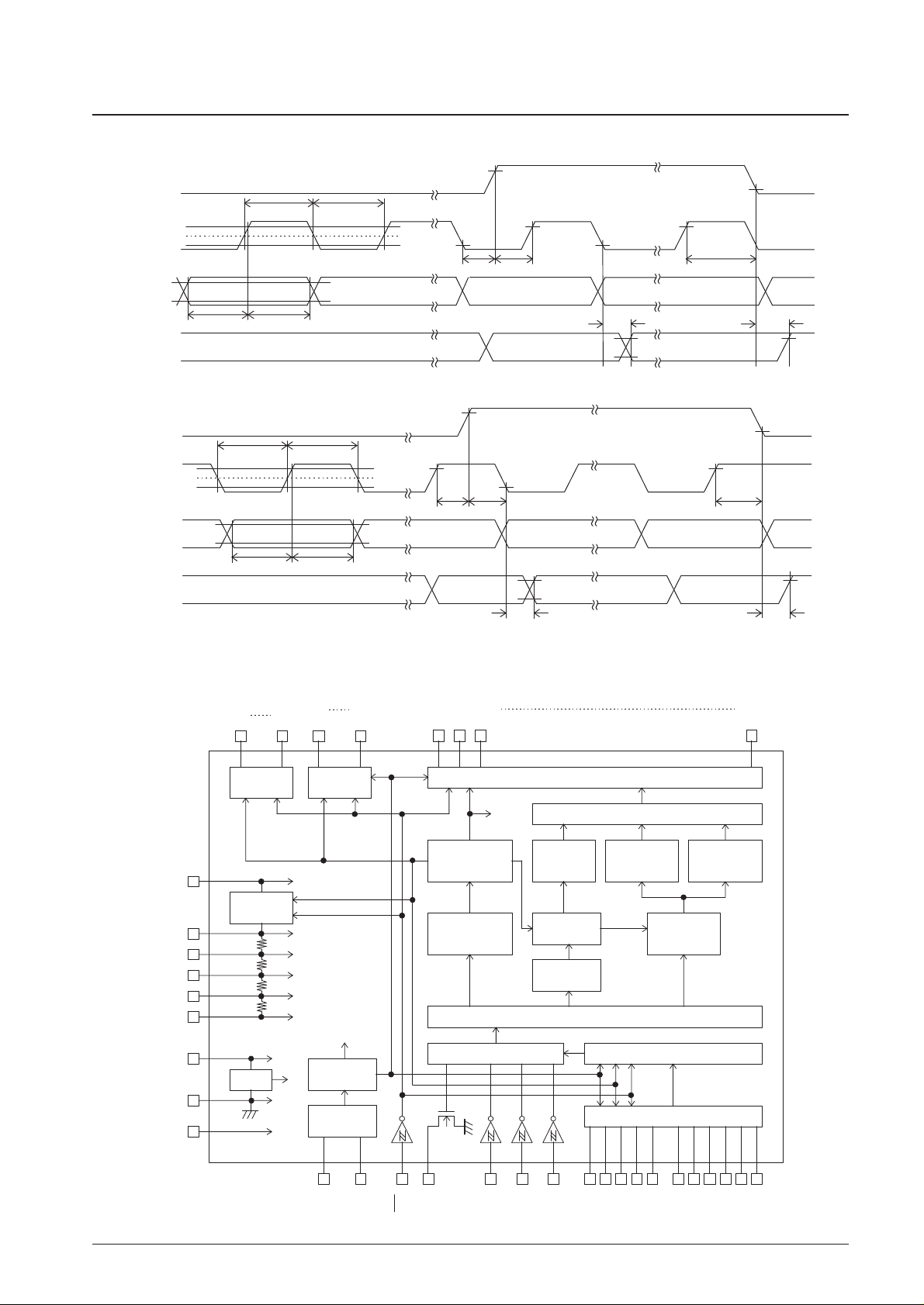
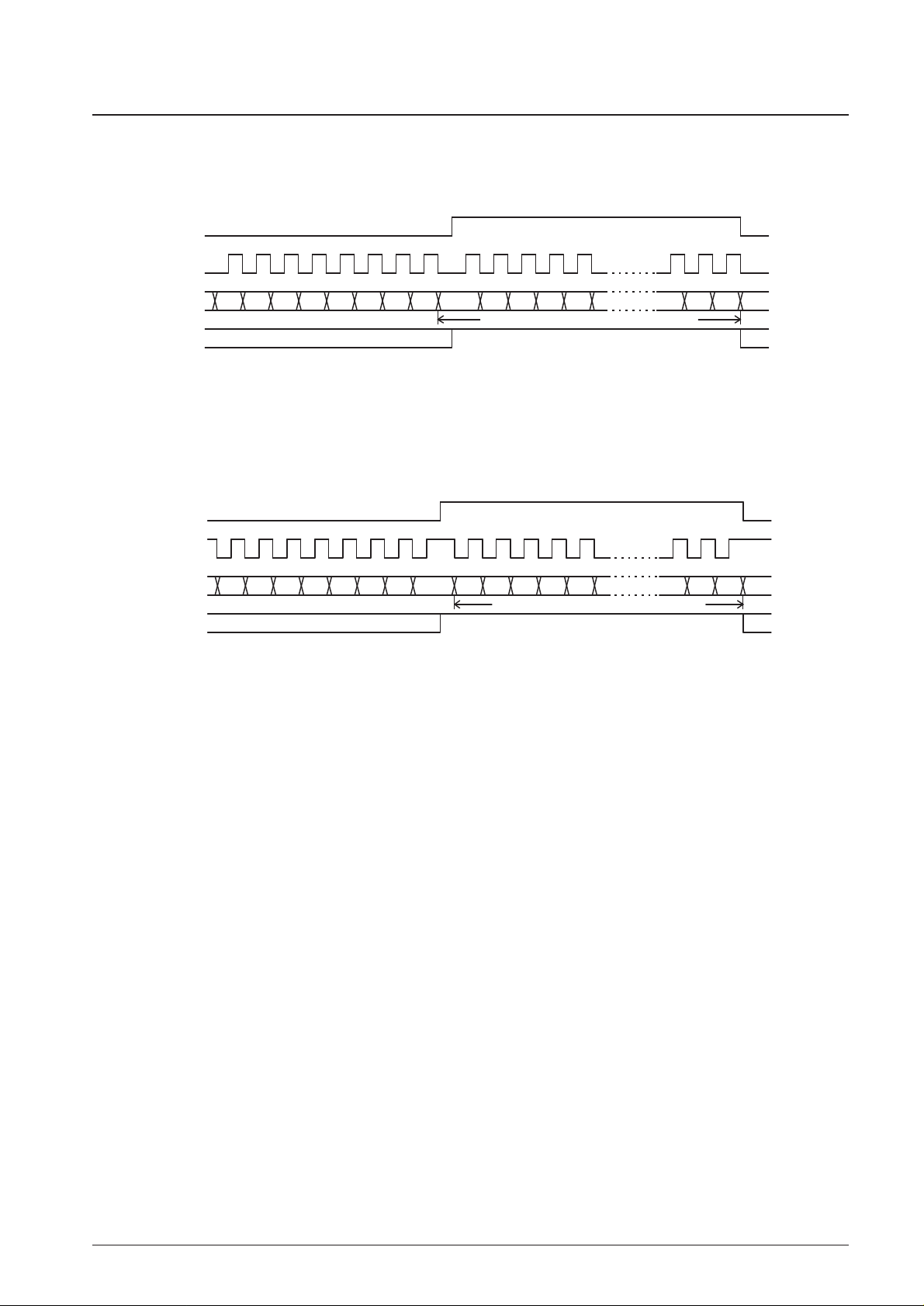
LC75817NE, 75817NW
• When CL is stopped at the low level
tdh
50%
VIH1
VIH1
VIL1
VIL1
VIH1
VIL1
tdr
tdc
tch
tcstcp
tds
CL
tøL
tøH
DO
DI
D1
D0
CE
• When CL is stopped at the high level
tøH
tøL
50%
VIH1
VIL1
tdh
VIH1
VIL1
VIH1
VIL1
tdr
tdc
tch
tcstcp
tds
CL
DO
DI
D1D0
CE
Block Diagram
S60/COM10
60
bits
CGRAM
5
× × × ×
×
9 16
bits
VDET
CLOCK
GENERATOR
CONTRAST
ADJUSTER
TIMING
GENERATOR
ADDRESS
REGISTER
INSTRUCTION
REGISTER
COMMON
DRIVER
INSTRUCTION
DECODER
ADDRESS
COUNTER
48 8
bits
CGROM
5 9 240
bits
S H I F T R E G I S T E R
L A T C H
S E G M E N T D R I V E R
OSCI
OSCO
INH
DO
DI
KS1
KS2
KS3
KS4
KS5
KS6
CE
KI1
KI2
KI3
KI4
KI5
CL
S1
S58
COM9
COM1
S59
KEY BUFFER
CCB INTERFACE
KEY SCAN
VDD
VLCD4
VLCD3
VLCD2
VLCD1
VLCD
VLCD0
GENERAL
PORT
P4
P1
VSS
TEST
Figure 2
ADRAM
DCRAM

No. 6144-7/43
LC75817NE, 75817NW
Pin Functions
Pin
Pin No.
Function Active I/O Handling when unused
LC75817NE LC75817NW
Segment driver outputs.
The S60/COM10 pin can be used as common driver output
under the “set display technique” instruction.
OPEN— O
S1 to S59
S60/COM10
3 to 61621 to 59
60
Common driver outputs. OPEN— OCOM1 to COM9 71 to 63 69 to 61
Oscillator connections. An oscillator circuit is formed by
connecting an external resistor and capacitor at these pins.
GND— IOSCI 97 95
Serial data interface connections to the controller. Note that DO,
being an open-drain output, requires a pull-up resistor.
CE : Chip enable
CL : Synchronization clock
DI : Transfer data
DO: Output data
GND
H ICE 100 98
ICL 1 99
— IDI 2 100
OPEN— OOSCO 96 94
Input that turns the display off, disables key scanning, and
forces the general-purpose output ports low.
• When INH is low (V
SS
):
• Display off
S1 to S59 = “L” (V
LCD
4).
S60/COM10 = “L” (V
LCD
4).
COM1 to COM9 = “L” (V
LCD
4).
• General-purpose output ports P1 to P4 = low (V
SS
)
• Key scanning disabled: KS1 to KS6 = low (V
SS
)
• All the key data is reset to low.
• When INH is high (V
DD
):
• Display on
• The state of the general-purpose output ports can
be set by executing a "Set general-purpose output
port state" instruction.
• Key scanning is enabled.
However, serial data can be transferred when the INH pin is
low.
V
DD
L IINH 98 96
LCD drive 3/4 bias voltage (middle level) supply pin. This pin can
be used to supply the 3/4 (V
LCD
0 – V
LCD
4) voltage level externally.
OPEN— I
V
LCD
1
90 88
LCD drive 2/4 bias voltage (middle level) supply pin. This pin can
be used to supply the 2/4 (V
LCD
0 - V
LCD
4) voltage level externally.
OPEN— I
V
LCD
2
91 89
LCD drive 1/4 bias voltage (middle level) supply pin. This pin can
be used to supply the 1/4 (V
LCD
0 – V
LCD
4) voltage level externally.
OPEN— I
V
LCD
3
92 90
Logic block power supply connection. Provide a voltage of
between 4.5 and 6.0 V.
—— —
V
DD
87 85
LCD driver block power supply connection. Provide a voltage of
between 7.0 and 10.0 V when the display contrast adjustment
circuit is used and provide a voltage of between 4.5 and 10.0 V
when the circuit is not used.
—— —
V
LCD
88 86
Power supply connection. Connect to ground.
—— —
V
SS
94 92
Key scan outputs. Although normal key scan timing lines
require diodes to be inserted in the timing lines to prevent
shorts, since these outputs are unbalanced CMOS transistor
outputs, these outputs will not be damaged by shorting when
these outputs are used to form a key matrix.
OPEN— OKS1 to KS6 72 to 77 70 to 75
Key scan inputs.
These pins have built-in pull-down resistors.
GNDH IKI1 to KI5 78 to 82 76 to 80
General-purpose output ports OPEN— OP1 to P4 83 to 86 81 to 84
DO 99 97 — O OPEN
This pin must be connected to ground. —— I
TEST
95 93
LCD drive 4/4 bias voltage (high level) supply pin. The level on
this pin can be changed by the display contrast adjustment circuit.
However, (V
LCD
0 – V
LCD
4) must be greater than or equal to 4.5
V. Also, external power must not be applied to this pin since the
pin circuit includes the display contrast adjustment circuit.
OPEN—
O
V
LCD
0
89 87
LCD drive 0/4 bias voltage (low level) supply pin. Fine
adjustment of the display contrast can be implemented by
connecting an external variable resistor to this pin.
However, (V
LCD
0 – V
LCD
4) must be greater than or equal to 4.5
V, and VLCD4 must be in the range 0 V to 1.5 V, inclusive.
GND— I
V
LCD
4
93 91
No. 6144-8/43
LC75817NE, 75817NW
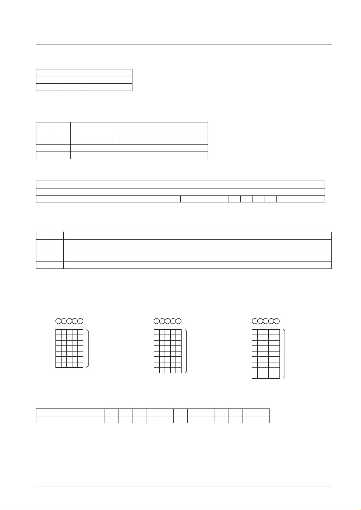
Block Functions
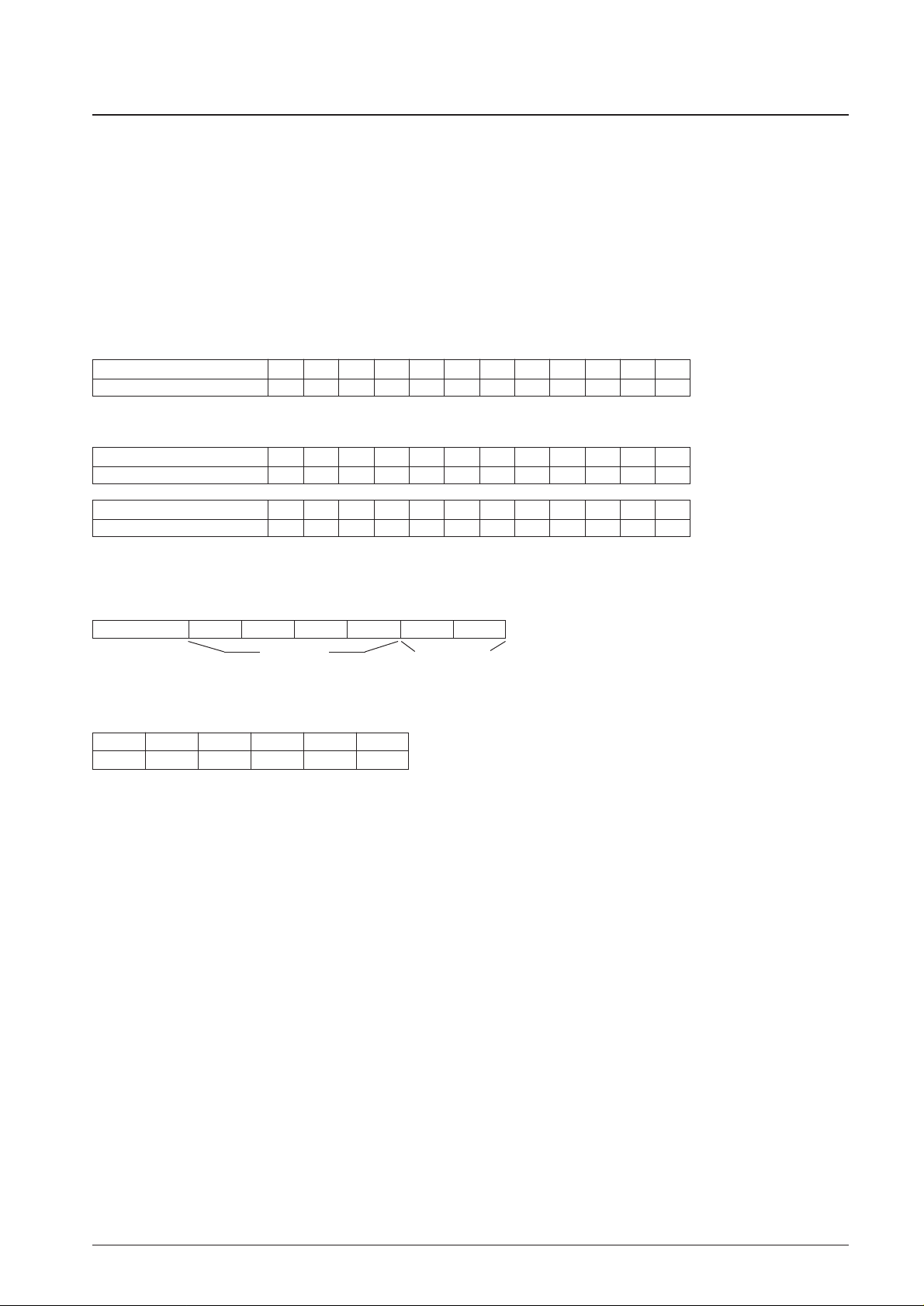
• AC (address counter)
AC is a counter that provides the addresses used for DCRAM and ADRAM.
The address is automatically modified internally, and the LCD display state is retained.
• DCRAM (data control RAM)
DCRAM is RAM that is used to store display data expressed as 8-bit character codes. (These character codes are
converted to 5 × 7, 5 × 8, or 5 × 9 dot matrix character patterns using CGROM or CGRAM.) DCRAM has a capacity of
48 × 8 bits, and can hold 48 characters. The table below lists the correspondence between the 6-bit DCRAM address
loaded into AC and the display position on the LCD panel.
•
When the DCRAM address loaded into AC is 00H.
Display digit 1 2 3 4 5 6 7 8 9 10 11 12
DCRAM address (hexadecimal) 00 01 02 03 04 05 06 07 08 09 0A 0B
However, when the display shift is performed by specifying MDATA, the DCRAM address shifts as shown below.
Note: *3. The DCRAM address is expressed in hexadecimal.
Example: When the DCRAM address is 2EH.
Note: *4. 5 × 7 dots ... 12-digit display 5 × 7 dots
5 × 8 dots ... 12-digit display 5 × 8 dots
5 × 9 dots ... 12-digit display 4 × 9 dots
Display digit 1 2 3 4 5 6 7 8 9 10 11 12
DCRAM address (hexadecimal) 01 02 03 04 05 06 07 08 09 0A 0B 0C
(Shift left)
Display digit 1 2 3 4 5 6 7 8 9 10 11 12
DCRAM address (hexadecimal) 2F 00 01 02 03 04 05 06 07 08 09 0A
DCRAM address DA0 DA1 DA2 DA3 DA4 DA5
(Shift right)
Least significant bit
↓
LSB
DA0 DA1 DA2 DA3 DA4 DA5
0 1 1 1 0 1
Most significant bit
↓
MSB
HexadecimalHexadecimal
No. 6144-9/43
LC75817NE, 75817NW
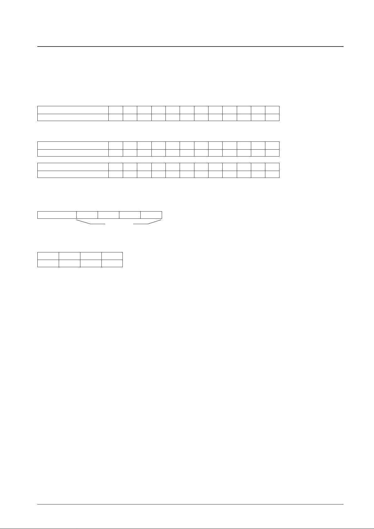
• ADRAM (Additional data RAM)
ADRAM is RAM that is used to store the ADATA display data. ADRAM has a capacity of 12 × 5 bits, and the stored
display data is displayed directly without the use of CGROM or CGRAM. The table below lists the correspondence
between the 4-bit ADRAM address loaded into AC and the display position on the LCD panel.
•
When the ADRAM address loaded into AC is 0H. (Number of digit displayed: 12)
Display digit 1 2 3 4 5 6 7 8 9 10 11 12
ADRAM address (hexadecimal) 0 1 2 3 4 5 6 7 8 9 A B
However, when the display shift is performed by specifying ADATA, the ADRAM address shifts as shown below.
Display digit 1 2 3 4 5 6 7 8 9 10 11 12
ADRAM address (hexadecimal) 1 2 3 4 5 6 7 8 9 A B 0
(Shift left)
Display digit 1 2 3 4 5 6 7 8 9 10 11 12
ADRAM address (hexadecimal) B 0 1 2 3 4 5 6 7 8 9 A
(Shift right)
Note: *5. The ADRAM address is expressed in hexadecimal.
Example: When the ADRAM address is A
H
Note: *6. 5 × 7 dots ... 12-digit display 5 dots
5 × 8 dots ... 12-digit display 5 dots
5 × 9 dots ... 12-digit display 4 dots
• CGROM (Character generator ROM)
CGROM is ROM that is used to generate the 240 kinds of 5 × 7, 5 × 8, or 5 × 9 dot matrix character patterns from the
8-bit character codes. CGROM has a capacity of 240 × 45 bits. When a character code is written to DCRAM, the
character pattern stored in CGROM corresponding to the character code is displayed at the position on the LCD
corresponding to the DCRAM address loaded into AC.
• CGRAM (Character generator RAM)
CGRAM is RAM to which user programs can freely write arbitrary character patterns. Up to 16 kinds of 5 × 7, 5 × 8,
or 5 × 9 dot matrix character patterns can be stored. CGRAM has a capacity of 16 × 45 bits.
ADRAM address RA0 RA1 RA2 RA3
RA0 RA1 RA2 RA3
0 1 0 1
Hexadecimal
Least significant bit
↓
LSB
Most significant bit
↓
MSB
No. 6144-10/43
LC75817NE, 75817NW
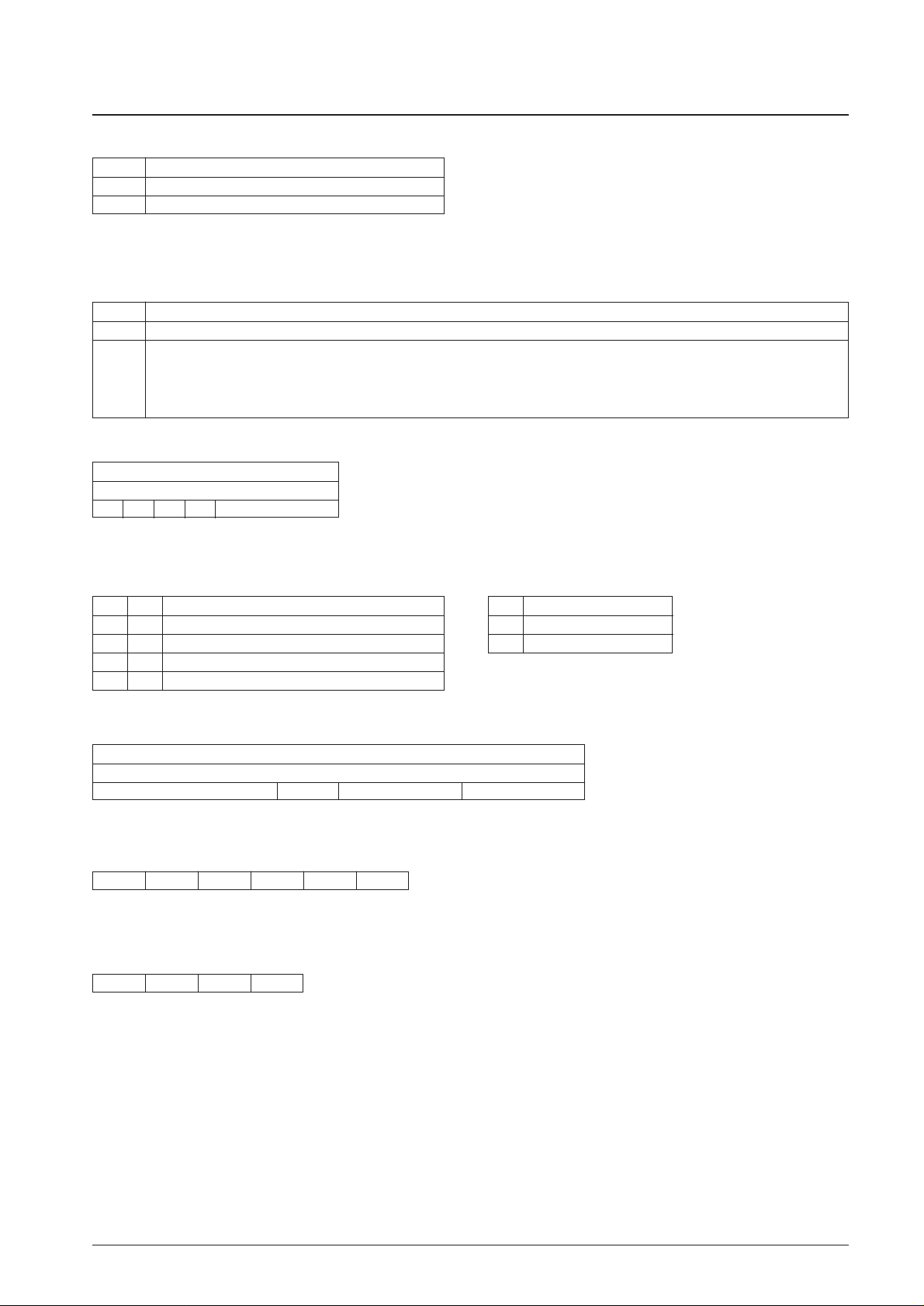
Serial Data Input
• When CL is stopped at the low level
D63D62
D4D3D21 0000010 D0 D1
CE
CL
DI
DO
• When CL is stopped at the high level
•
B0 to B3, A0 to A3: CCB address 42H
•
D0 to D63: Instruction data
The data is acquired on the rising edge of the CL signal and latched on the falling edge of the CE signal. When
transferring instruction data from the microcontroller, applications must assure that the time from the transfer of one set
of instruction data until the next instruction data transfer is significantly longer than the instruction execution time.
D63D62
D4D3D20000 1010 D0 D1
CE
DI
DO
CL
Instruction data (Up to 64 bits)
Instruction data (Up to 64 bits)
A3A2A1A0B3B2B1B0
A3A2A1A0B3B2B1B0

No. 6144-11/43
LC75817NE, 75817NW
Instruction Table
Notes: *7. The data format differs when the “DCRAM data write” instruction is executed in the increment mode (IM = 1).
(See detailed instruction descriptions .)
*8. The data format differs when the “ADRAM data write” instruction is executed in the increment mode (IM = 1).
(See detailed instruction descriptions.)
*9. The execution times listed here apply when fosc = 300 kHz. The execution times differ when the oscillator frequency fosc differs.
Example: When fosc = 210 kHz
300
27 µs ×—— = 39 µs
210
*10.When the sleep mode (SP = 1) is set, the execution time is 27 µs (when f
osc
= 300 kHz).
Instruction D0 D1...D39 D40 D41 D42 D43 D44 D45 D46 D47 D48 D49 D50 D51 D52 D53 D54 D55 Execution time *
9
Set display technique
Display on/off control DG1 DG2 DG3 DG4 DG5 DG6 DG7 DG8 DG9 DG10 DG11 DG12 X X X X
Display shift
Set AC address DA0 DA1 DA2 DA3 DA4 DA5 X X
DCRAM data write *
7
AC0 AC1 AC2 AC3 AC4 AC5 AC6 AC7 DA0 DA1 DA2 DA3 DA4 DA5 X X
ADRAM data write *
8
AD1 AD2 AD3 AD4 AD5 X X X RA0 RA1 RA2 RA3 X X X X
CGRAM data write CD1 CD2...CD40 CD41 CD42 CD43 CD44 CD45 X X X CA0 CA1 CA2 CA3 CA4 CA5 CA6 CA7
Set display contrast CT0 CT1 CT2 CT3 X X X X
Set key scan output state
KC1 KC2 KC3 KC4 KC5 KC6 X X
Set general-purpose output port state
D56 D57 D58 D59 D60 D61 D62 D63
DT1 DT2 X X 0 0 0 1 0 µs
M A SC SP 0 0 1 0 0 µs/27 µs *
10
M A R/L X 0 0 1 1 27 µs
RA0 RA1 RA2 RA3 0 1 0 0 27 µs
IM X X X 0 1 0 1 27 µs
IM X X X 0 1 1 0 27 µs
X X X X 0 1 1 1 27 µs
CTC X X X 1 0 0 0 0 µs
X X X X 1 0 0 1 0 µs
PC1 PC2 PC3 PC4 1 0 1 0 0 µs
X: don’t care
No. 6144-12/43
LC75817NE, 75817NW
Detailed Instruction Descriptions
• Set display technique ... <Sets the display technique>
Code
D56 D57 D58 D59 D60 D61 D62 D63
DT1 DT2 X X 0 0 0 1
X: don’t care
X: don’t care
Note: *11 S60: Segment outputs
COMn (n = 9, 10): Common outputs
DT1, DT2: Sets the display technique
DT1 DT2 Display technique
Output pins
COM9 S60/COM10
0 0 1/8 duty, 1/4 bias drive
Fixed at the V
LCD
4 level
S60
1 0 1/9 duty, 1/4 bias drive COM9 S60
0 1 1/10 duty, 1/4 bias drive COM9 COM10
• Display on/off control ... <Turns the display on or off>
Code
D40 D41 D42 D43 D44 D45 D46 D47 D48 D49 D50 D51 D52 D53 D54 D55 D56 D57 D58 D59
DG1 DG2 DG3 DG4 DG5 DG6 DG7 DG8 DG9 DG10 DG11 DG12 X X X X M A SC SP
D60 D61 D62 D63
0 0 1 0
M, A: Specifies the data to be turned on or off
Note: *12. MDATA, ADATA
5 × 7 dot matrix display 5 × 8 dot matrix display 5 ×9 dot matrix display
M A Display operating state
0 0 Both MDATA and ADATA are turned off (The display is forcibly turned off regardless of the DG1 to DG12 data.)
0 1 Only ADATA is turned on (The ADATA of display digits specified by the DG1 to DG12 data are turned on.)
1 0 Only MDATA is turned on (The MDATA of display digits specified by the DG1 to DG12 data are turned on.)
1 1 Both MDATA and ADATA are turned on (The MDATA and ADATA of display digits specified by the DG1 to DG12 data are turned on.)
DG1 to DG12: Specifies the display digit
For example, if DG1 to DG6 are 1, and DG7 to DG12 are 0, then display digits 1 to 6 will be turned on, and display digits 7
to 12 will be turned off (blanked).
Display digit 1 2 3 4 5 6 7 8 9 10 11 12
Display digit data DG1 DG2 DG3 DG4 DG5 DG6 DG7 DG8 DG9 DG10 DG11 DG12
. . . .
. . .
ADATA
MDATA
. . . .
. . .
ADATA
MDATA
. . . .
. . .
ADATA
MDATA
No. 6144-13/43
LC75817NE, 75817NW
SC: Controls the common and segment output pins
Note: *13. When SC is 1, the S1 to S60 and COM1 to COM10 output pins are set to the V
LCD
4 level, regardless of the M, A, and DG1 to DG12 data.
SC Common and segment output pin states
0 Output of LCD drive waveforms
1 Fixed at the V
LCD
4 level (all segments off)
SP: Controls the normal mode and sleep mode
SP Mode
0 Normal mode
Sleep mode
1
The common and segment pins go to the V
LCD
4 level and the oscillator on the OSCI, OSCO pins is stopped (although it operates during key
scan operations) to reduce current drain. Although the “display on/off control”, “set display contrast”, “set key scan output state”, and “set
general-purpose output port state” instructions can be executed in this mode, applications must return the IC to normal mode to execute any of
the other instruction settings.
• Display shift ... <Shifts the display>
Code
D56 D57 D58 D59 D60 D61 D62 D63
M A R/L X 0 0 1 1
X: don’t care
M, A: Specifies the data to be shifted
M A Shift operating state
0 0 Neither MDATA nor ADATA is shifted
0 1 Only ADATA is shifted
1 0 Only MDATA is shifted
1 1 Both MDATA and ADATA are shifted
R/L: Specifies the shift direction
R/L Shift direction
0 Shift left
1 Shift right
X: don’t care
• Set AC address... <Specifies the DCRAM and ADRAM address for AC>
Code
D48 D49 D50 D51 D52 D53 D54 D55 D56 D57 D58 D59 D60 D61 D62 D63
DA0 DA1 DA2 DA3 DA4 DA5 X X RA0 RA1 RA2 RA3 0 1 0 0
DA0 to DA5: DCRAM address
DA0 DA1 DA2 DA3 DA4 DA5
LSB
↑
Least significant bit
MSB
↑
Most significant bit
RA0 to RA3: ADRAM address
RA0 RA1 RA2 RA3
LSB
↑
Least significant bit
MSB
↑
Most significant bit
This instruction loads the 6-bit DCRAM address DA0 to DA5 and the 4-bit ADRAM address RA0 to RA3 into the AC.
 Loading...