


Ordering number : EN5915A
N1098RM (OT) No. 5915-1/27
LC75811E, 75811W
SANYO Electric Co.,Ltd. Semiconductor Bussiness Headquarters
TOKYO OFFICE Tokyo Bldg., 1-10, 1 Chome, Ueno, Taito-ku, TOKYO, 110-8534 JAPAN
1/8 to 1/10 Duty Dot Matrix LCD Display Controller/Driver
CMOS IC
Any and all SANYO products described or contained herein do not have specifications that can handle
applications that require extremely high levels of reliability, such as life-support systems, aircraft’s
control systems, or other applications whose failure can be reasonably expected to result in serious
physical and/or material damage. Consult with your SANYO representative nearest you before using
any SANYO products described or contained herein in such applications.
SANYO assumes no responsibility for equipment failures that result from using products at values that
exceed, even momentarily, rated values (such as maximum ratings, operating condition ranges, or other
parameters) listed in products specifications of any and all SANYO products described or contained
herein.
• CCB is a trademark of SANYO ELECTRIC CO., LTD.
• CCB is SANYO’s original bus format and all the bus
addresses are controlled by SANYO.
Overview
The LC75811E and LC75811W are 1/8 to 1/10 duty dot
matrix LCD display controller/drivers that supports the
display of characters, numbers, and symbols. In addition to
generating dot matrix LCD drive signals based on data
transferred serially from a microcontroller, the LC75811E
and LC75811W also provide on-chip character display ROM
and RAM to allow display systems to be implemented easily.
Features
• Controls and drives a 5 ×7, 5 × 8, or 5 × 9 dot matrix LCD.
• Supports accessory display segment drive (up to 60
segments)
• Display technique: 1/8 duty 1/4 bias drive (5 × 7 dots)
1/9 duty 1/4 bias drive (5 × 8 dots)
1/10 duty 1/4 bias drive (5 × 9 dots)
• Display digits: 12 digits ×1 line (5 × 7 dots),
11 digits × 1 line (5 × 8 or 5 × 9 dots)
• Display control memory
CGROM: 240 characters (5 × 7, 5 × 8, or 5 × 9 dots)
CGRAM: 16 characters (5 × 7, 5 × 8, or 5 × 9 dots)
ADRAM: 12 × 5 bits
DCRAM: 48 × 8 bits
• Instruction function
Display on/off control
Display shift function
• Provides a backup function based on low power modes.
• Serial data input supports CCB format communication
with the system controller.
• Independent LCD drive block power supply VLCD
• Provides a RES pin for LSI internal initialization
• RC oscillator circuit
Package Dimensions
unit: mm
3174-QFP80E
unit: mm
3220-SQFP80
SANYO: QFP80E
[LC75811E]
SANYO: SQFP80
[LC75811W]
No. 5915-2/27
LC75811E, 75811W
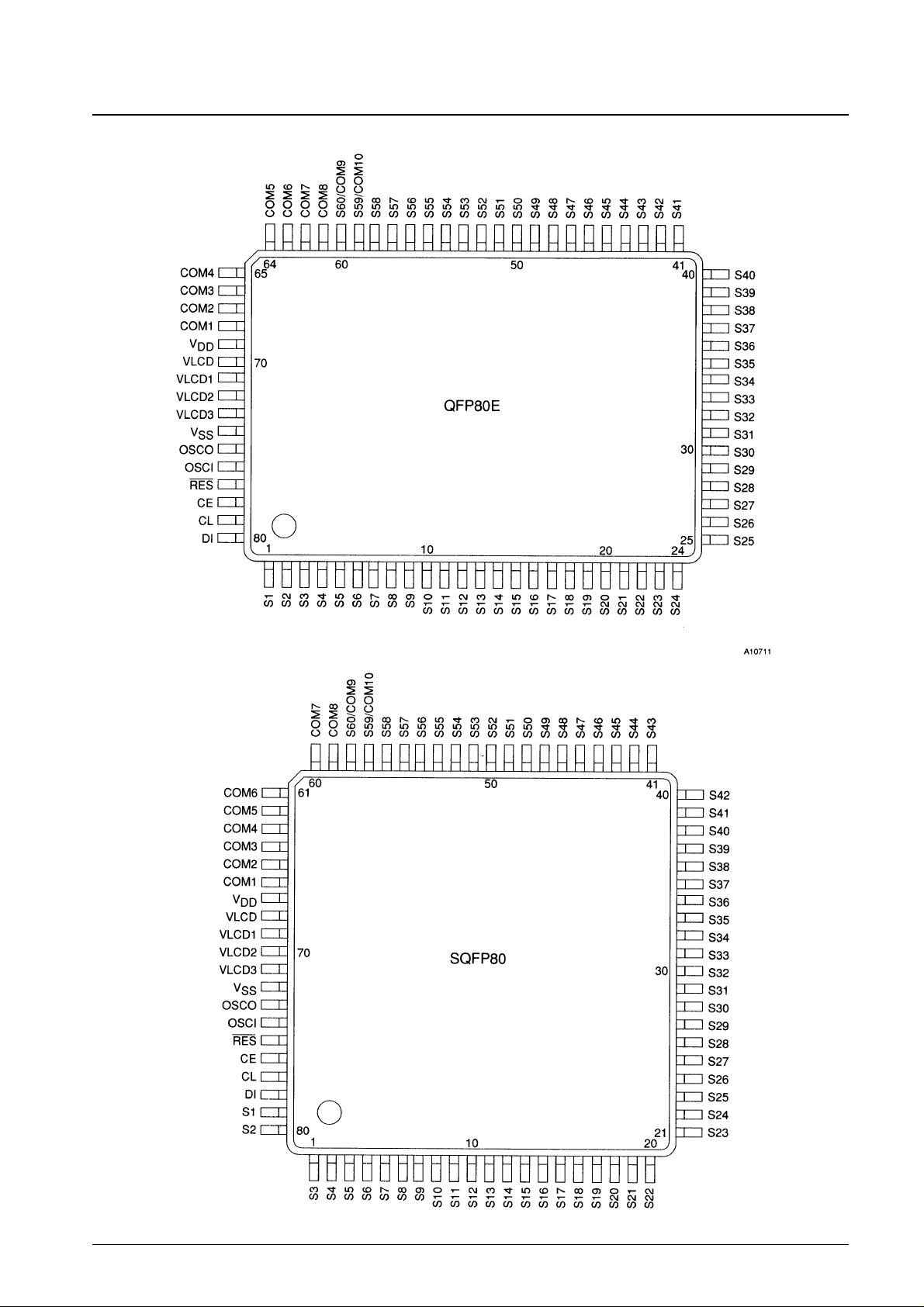
Pin Assignments (Top View)
LC75811E
LC75811W
No. 5915-3/27
LC75811E, 75811W
Parameter Symbol Conditions Ratings Unit
Maximum supply voltage
V
DD
max V
DD
–0.3 to +7.0 V
V
LCD
max V
LCD
–0.3 to +11.0 V
V
IN
1 CE, CL, DI, RES –0.3 to +7.0 V
Input voltage V
IN
2 OSCI –0.3 to VDD+ 0.3 V
V
IN
3 V
LCD
1, V
LCD
2, V
LCD
3 –0.3 to V
LCD
+ 0.3 V
Output voltage
V
OUT
1 OSCO –0.3 to VDD+ 0.3 V
V
OUT
2 S1 to S60, COM1 to COM10 –0.3 to V
LCD
+ 0.3 V
Output current
I
OUT
1 S1 to S60 300 µA
I
OUT
2 COM1 to COM10 3 mA
Allowable power dissipation Pd max Ta = 85°C 200 mW
Operating temperature Topr –40 to +85 °C
Storage temperature Tstg –55 to +125 °C
Specifications
Absolute Maximum Ratings at Ta = 25°C, VSS= 0 V
Parameter Symbol Conditions
Ratings
Unit
min typ max
Supply voltage
V
DD
V
DD
2.7 6.0 V
V
LCDVLCD
4.5 10.0 V
V
LCD
1 V
LCD
1 3/4 V
LCD
V
LCD
V
Input voltage V
LCD
2 V
LCD
2 2/4 V
LCD
V
LCD
V
V
LCD
3 V
LCD
3 1/4 V
LCD
V
LCD
V
Input high level voltage
V
IH
1 CE, CL, DI, RES 0.8 V
DD
6.0 V
V
IH
2 OSCI 0.7 V
DD
V
DD
V
Input low level voltage
V
IL
1 CE, CL, DI, RES 0 0.2 V
DD
V
V
IL
2 OSCI 0 0.3 V
DD
V
Recommended external resistance R
OSC
OSCI, OSCO 33 kΩ
Recommended external capacitance C
OSC
OSCI, OSCO 220 pF
Guaranteed oscillation range f
OSC
OSC 150 300 600 kHz
Data setup time t
ds
CL, DI: Figure 2 160 ns
Data hold time t
dh
CL, DI: Figure 2 160 ns
CE wait time t
cp
CE, CL: Figure 2 160 ns
CE setup time t
cs
CE, CL: Figure 2 160 ns
CE hold time t
ch
CE, CL: Figure 2 160 ns
High level clock pulse width tøH CL: Figure 2 160 ns
Low level clock pulse width tøL CL: Figure 2 160 ns
Minimum reset pulse width t
WRES
RES: Figure 3 1 µs
Allowable Operating Ranges at Ta = –40 to 85°C, VSS= 0 V
No. 5915-4/27
LC75811E, 75811W
Parameter Symbol Conditions
Ratings
Unit
min typ max
Hysteresis V
H
CE, CL, DI, RES 0.1 V
DD
V
Input high level current I
IH
CE, CL, DI, RES, OSCI: VI= 6.0 V 5.0 µA
Input low level current I
IL
CE, CL, DI, RES, OSCI: VI= 0 V –5.0 µA
V
OH
1 S1 to S60: IO= –20 µA V
LCD
– 0.6 V
Output high level voltage V
OH
2 COM1 to COM10: IO= –100 µA V
LCD
– 0.6 V
V
OH
3 OSCO: IO= –500 µA VDD– 1.0 V
V
OL
1 S1 to S60: IO= 20 µA 0.6 V
Output low level voltage V
OL
2 COM1 to COM10: IO= 100 µA 0.6 V
V
OL
3 OSCO: IO= 500 µA 1.0 V
V
MID
1 S1 to S60: IO±20 µA
2/4 V
LCD
– 0.6 2/4 V
LCD
+ 0.6
V
Output middle level voltage*1 V
MID
2 COM1 to COM10: IO= ±100 µA
3/4 V
LCD
– 0.6 3/4 V
LCD
+ 0.6
V
V
MID
3 COM1 to COM10: IO= ±100 µA
1/4 V
LCD
– 0.6 1/4 V
LCD
+ 0.6
V
Oscillator frequency f
OSC
OSCI, OSCO: R
OSC
= 33 kΩ, C
OSC
= 220 pF 210 300 390 kHz
I
DD
1 VDD: power saving mode 5 µA
Current drain
I
DD
2 VDD: VDD= 6.0 V, output open, f
OSC
= 300 kHz 450 900 µA
I
LCD
1 V
LCD
: power saving mode 5 µA
I
LCD
2 V
LCD
: V
LCD
= 10.0 V, output open, f
OSC
= 300 kHz 200 400 µA
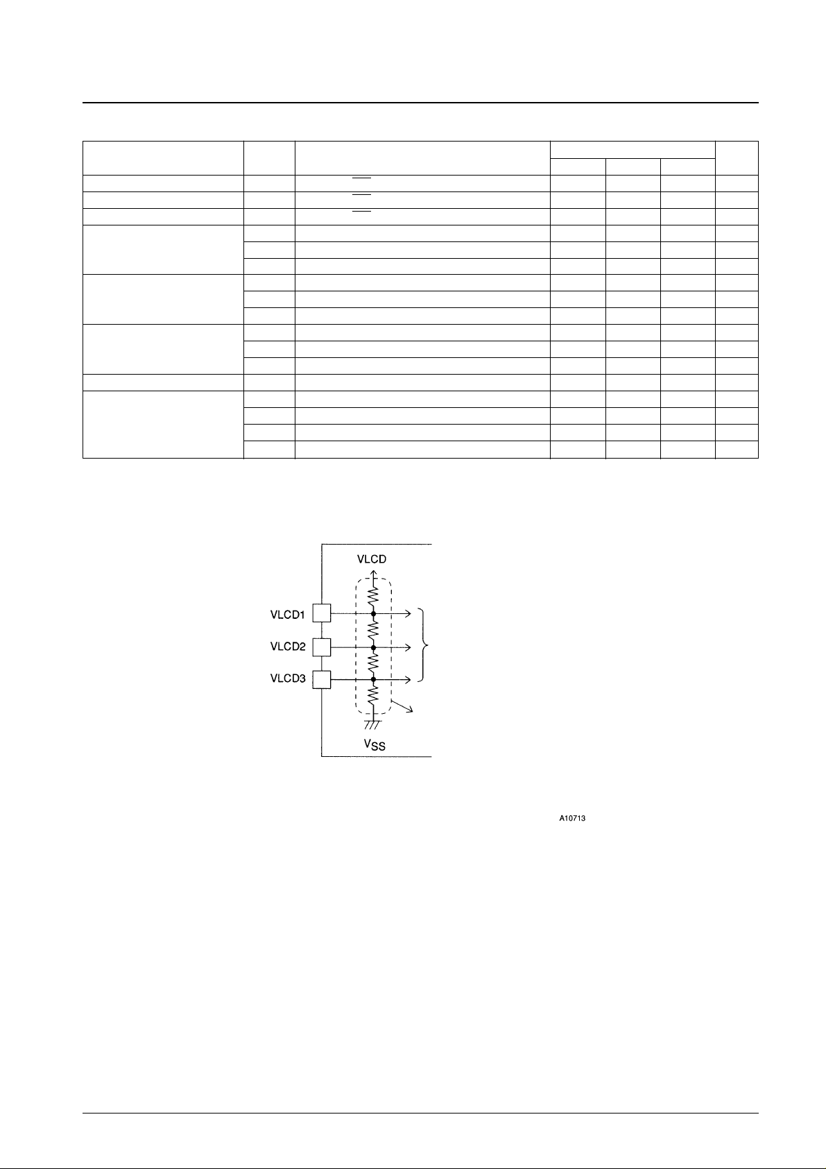
Electrical Characteristics in the Allowable Operating Ranges
Note *1: Excluding the bias voltage generation divider resistor built into the V
LCD
1, V
LCD
2, and V
LCD
3. (See figure 1.)
Excluding these resistors
To the common and segment drivers
Figure 1

No. 5915-5/27
LC75811E, 75811W
• When CL is stopped at the low level
• When CL is stopped at the high level
Block Diagram
Figure 2
No. 5915-6/27
LC75811E, 75811W
Pin Functions
Pin
Pin No.
Function Active I/O Handling when unused
LC75811E LC75811W
Segment driver outputs.
The S59/COM10 and S60/COM9 pins can be used as common
driver outputs under the “set display technique” instruction.
OPEN— O
S1 to S58
S59/COM10
S60/COM9
1 to 58
59
60
79, 80
1 to 56
57
58
Common driver outputs. OPEN— OCOM1 to COM8 68 to 61 66 to 59
Oscillator connections. An oscillator circuit is formed by
connecting an external resistor and capacitor at these pins.
GND— IOSCI 76 74
Serial data transfer inputs. These pins are connected to the
microcontroller.
CE: Chip enable
CL: Synchronization clock
DI: Transfer data
GND
H ICE 78 76
ICL 79 77
— IDI 80 78
OPEN— OOSCO 75 73
Reset signal input.
• When RES is low (V
SS
):
• Display off
S1 to S58 = “L” (V
SS
).
S59/COM10 and S60/COM9 = “L” (V
SS
).
COM1 to COM8 = “L” (V
SS
).
• Serial data transfer is disabled.
• The OSCI/OSCO pin oscillator is stopped.
• When RES is high (V
DD
):
• Display on after a “display on/off control” (display on
state setting) instruction is executed.
• Serial data transfers are enabled.
• The OSCI/OSCO pin oscillator operates.
GNDL IRES 77 75
Used for applying the LCD drive 3/4 bias voltage externally. OPEN— I
V
LCD
1
71 69
Used for applying the LCD drive 2/4 bias voltage externally. OPEN— I
V
LCD
2
72 70
Used for applying the LCD drive 1/4 bias voltage externally. OPEN— I
V
LCD
3
73 71
Logic block power supply connection. Provide a voltage of
between 2.7 and 6.0 V.
—— —
V
DD
69 67
LCD driver block power supply connection. Provide a voltage of
between 4.5 and 10.0 V.
—— —
V
LCD
70 68
Power supply connection. Connect to ground. —— —
V
SS
74 72

No. 5915-7/27
LC75811E, 75811W
Block Functions
• AC (address counter)
AC is a counter that provides the addresses used for DCRAM and ADRAM.
The address is automatically modified internally, and the LCD display state is retained.
• DCRAM (data control RAM)
DCRAM is RAM that is used to store display data expressed as 8-bit character codes. (These character codes are
converted to 5 × 7, 5 × 8, or 5 × 9 dot matrix character patterns using CGROM or CGRAM.) DCRAM has a capacity of
48 × 8 bits, and can hold 48 characters. The table below lists the correspondence between the 6-bit DCRAM address
loaded into AC and the display position on the LCD panel.
• When the DCRAM address loaded into AC is 00H.
Display digit 1 2 3 4 5 6 7 8 9 10 11 12
DCRAM address (hexadecimal) 00 01 02 03 04 05 06 07 08 09 0A 0B
However, when the display shift is performed by specifying MDATA, the DCRAM address shifts as shown below.
Note:*2. The DCRAM addresses are expressed in hexadecimal.
Example: When the DCRAM address is 2EH.
Note:*3. 5 × 7 dots ... 12-digit display 5 × 7 dots
5 × 8 dots ... 12-digit display 4 × 8 dots
5 × 9 dots ... 12-digit display 3 × 9 dots
Display digit 1 2 3 4 5 6 7 8 9 10 11 12
DCRAM address (hexadecimal) 01 02 03 04 05 06 07 08 09 0A 0B 0C
(Left shift)
Display digit 1 2 3 4 5 6 7 8 9 10 11 12
DCRAM address (hexadecimal) 2F 00 01 02 03 04 05 06 07 08 09 0A
DCRAM address DA0 DA1 DA2 DA3 DA4 DA5
(Right shift)
LSB
DA0 DA1 DA2 DA3 DA4 DA5
0 1 1 1 0 1
MSB
Least significant bit Most significant bit
HexadecimalHexadecimal
No. 5915-8/27
LC75811E, 75811W
• ADRAM (Additional data RAM)
ADRAM is RAM used to store the ADATA display data. ADRAM has a capacity of 12 × 5 bits, and the stored display
data is displayed directly without the use of CGROM or CGRAM. The table below lists the correspondence between
the 4-bit ADRAM address loaded into AC and the display position on the LCD panel.
• When the ADRAM address loaded into AC is 0H. (Number of digit displayed: 12)
Display digit 1 2 3 4 5 6 7 8 9 10 11 12
ADRAM address (hexadecimal) 0 1 2 3 4 5 6 7 8 9 A B
However, when the display shift is performed by specifying ADATA, the ADRAM address shifts as shown below.
Display digit 1 2 3 4 5 6 7 8 9 10 11 12
ADRAM address (hexadecimal) 1 2 3 4 5 6 7 8 9 A B 0
(Left shift)
Display digit 1 2 3 4 5 6 7 8 9 10 11 12
ADRAM address (hexadecimal) B 0 1 2 3 4 5 6 7 8 9 A
(Right shift)
Note: *4. The ADRAM addresses are expressed in hexadecimal.
Example: When the ADRAM address is A
H
Note: *5. 5 × 7 dots ... 12-digit display 5 dots
5 × 8 dots ... 12-digit display 4 dots
5 × 9 dots ... 12-digit display 3 dots
• CGROM (Character generator ROM)
CGROM is ROM used to generate the 240 kinds of 5 × 7, 5 × 8, or 5 × 9 dot matrix character patterns from the 8-bit
character codes. CGROM has a capacity of 240 × 45 bits. When a character code is written to DCRAM, the character
pattern stored in CGROM corresponding to the character code is displayed at the position on the LCD corresponding to
the DCRAM address loaded into AC.
• CGRAM (Character generator RAM)
CGRAM is RAM to which user programs can freely write arbitrary character patterns. Up to 16 kinds of 5 × 7, 5 × 8,
or 5 × 9 dot matrix character patterns can be stored. CGRAM has a capacity of 16 × 45 bits.
ADRAM address RA0 RA1 RA2 RA3
LSB
RA0 RA1 RA2 RA3
0 1 0 1
MSB
Least significant bit Most significant bit
Hexadecimal

No. 5915-9/27
LC75811E, 75811W
Reset Function
The LC75811E and LC75811W are reset when a low level is applied to the RES pin at power on and, in normal mode.
On a reset the LC75811E and LC75811W create a display with all LCD panels turned off. However, after a reset
applications must set the contents of DCRAM, ADRAM, and CGRAM before turning on display with a “display on/off
control” instruction since the contents of these memories are undefined. That is, applications must execute the following
instructions.
• Set display technique
• DCRAM data write
• ADRAM data write (If ADRAM is used.)
• CGRAM data write (If CGRAM is used.)
• Set AC address
After executing the above instructions, applications must turn on the display with a “display on/off control” instruction.
Note that when applications turn off in the normal mode, applications must turn off the display with a “display on/off
control” instruction. (See the detailed instruction descriptions.)
Serial Data Transfer Format
• When CL is stopped at the low level
Instruction data
Up to 64 bits
• When CL is stopped at the high level
• CCB address: 47H
• D0 to D63: Instruction data
The data is acquired on the rising edge of the CL signal and latched on the falling edge of the CE signal. When
transferring instruction data from the microcontroller, applications must assure that the time from the transfer of one set
of instruction data until the next instruction data transfer is significantly longer than the instruction execution time.
CCB address
8 bits
CCB address
8 bits
Instruction data
Up to 64 bits

No. 5915-10/27
LC75811E, 75811W
Instruction Table
Notes:*6.The data format differs when the “DCRAM data write” instruction is executed in the increment mode (IM = 1).
(See detailed instruction descriptions .)
*7.The data format differs when the “ADRAM data write” instruction is executed in the increment mode (IM = 1).
(See detailed instruction descriptions.)
*8.The execution times listed here apply when fosc = 300 kHz. The execution times differ when the oscillator frequency fosc differs.
Example: When fosc = 210 kHz
300
27 µs × —— = 39 µs
210
*9.When the power saving mode (BU = 1) is set, the execution time is 27 µs (when f
osc
= 300 kHz).
Instruction D0 D1...D39 D40 D41 D42 D43 D44 D45 D46 D47 D48 D49 D50 D51 D52 D53 D54 D55 Execution time *
8
Set display technique
Display on/off control DG1 DG2 DG3 DG4 DG5 DG6 DG7 DG8 DG9 DG10 DG11 DG12 X X X X
Display shift
Set AC address DA0 DA1 DA2 DA3 DA4 DA5 X X
DCRAM data write *
6
AC0 AC1 AC2 AC3 AC4 AC5 AC6 AC7 DA0 DA1 DA2 DA3 DA4 DA5 X X
ADRAM data write *
7
AD1 AD2 AD3 AD4 AD5 X X X RA0 RA1 RA2 RA3 X X X X
CGRAM data write CD1 CD2...CD40 CD41 CD42 CD43 CD44 CD45 X X X CA0 CA1 CA2 CA3 CA4 CA5 CA6 CA7
D56 D57 D58 D59 D60 D61 D62 D63
DT1 DT2 X X 0 0 0 1 0 µs
M A SC BU 0 0 1 0 0 µs/27 µs *
9
M A R/L X 0 0 1 1 27 µs
RA0 RA1 RA2 RA3 0 1 0 0 27 µs
IM X X X 0 1 0 1 27 µs
IM X X X 0 1 1 0 27 µs
X X X X 0 1 1 1 27 µs
X: don’t care

No. 5915-11/27
LC75811E, 75811W
Detailed Instruction Descriptions
• Set display technique ... <Sets the display technique>
Code
D56 D57 D58 D59 D60 D61 D62 D63
DT1 DT2 X X 0 0 0 1
X: don’t care
X: don’t care
Note: *10. Sn (n = 59, 60): Segment outputs
COMn (n = 9, 10): Common outputs
DT1, DT2: Setting the display technique
DT1 DT2 Display technique
Output pins
S60/COM9 S59/COM10
0 0 1/8 duty, 1/4 bias drive S60 S59
1 0 1/9 duty, 1/4 bias drive COM9 S59
0 1 1/10 duty, 1/4 bias drive COM9 COM10
• Display on/off control ... <Turns the display on or off>
Code
D40 D41 D42 D43 D44 D45 D46 D47 D48 D49 D50 D51 D52 D53 D54 D55 D56 D57 D58 D59
DG1 DG2 DG3 DG4 DG5 DG6 DG7 DG8 DG9 DG10 DG11 DG12 X X X X M A SC BU
D60 D61 D62 D63
0 0 1 0
M, A: Specifies the data to be turned on or off.
Note: *11. MDATA, ADATA
5 × 7 dot matrix display 5 × 8 dot matrix display 5 × 9 dot matrix display
M A Display operating state
0 0 Both MDATA and ADATA are turned off (The display is forcibly turned off regardless of the DG1 to DG12 data.)
0 1 Only ADATA is turned on (The ADATA of display digits specified by the DG1 to DG12 data are turned on.)
1 0 Only MDATA is turned on (The MDATA of display digits specified by the DG1 to DG12 data are turned on.)
1 1 Both MDATA and ADATA are turned on (The MDATA and ADATA of display digits specified by the DG1 to DG12 data are turned on.)
DG1 to DG12: Specifies the display digit
For example, if DG1 to DG6 are 1, and DG7 to DG12 are 0, then display digits 1 to 6 will be turned on, and display digits 7
to 12 will be turned off (blanked).
Display digit 1 2 3 4 5 6 7 8 9 10 11 12
Display digit data DG1 DG2 DG3 DG4 DG5 DG6 DG7 DG8 DG9 DG10 DG11 DG12

No. 5915-12/27
LC75811E, 75811W
SC: Controls the common and segment output pins.
Note: *12. When SC is 1, the S1 to S60 and COM1 to COM10 output pins are set to the VSS level, regardless of the M, A, and DG1 to DG12 data.
SC Common and segment output pin states
0 Output of LCD drive waveforms
1 Fixed at the V
SS
level (all segments off)
BU: Controls the normal mode and power saving mode.
BU Mode
0 Normal mode
Power saving mode
1
(In this mode, the OSCI and OSCO pins oscillator is stopped, and the common and segment pins are set to the V
SS
level. In this mode,
instructions other than the “display on/off control” instruction cannot be executed. Thus applications must set the LSI to normal mode before
executing any of the other instructions.)
• Display shift ... <Shifts the display>
Code
D56 D57 D58 D59 D60 D61 D62 D63
M A R/L X 0 0 1 1
X: don’t care
M, A: Specifies the data to be shifted
M A Shift operating state
0 0 Neither MDATA nor ADATA is shifted
0 1 Only ADATA is shifted
1 0 Only MDATA is shifted
1 1 Both MDATA and ADATA are shifted
R/L: Shift direction specification
R/L Shift direction
0 Left shift
1 Right shift
X: don’t care
• Set AC address... <Specifies the DCRAM and ADRAM address for AC>
Code
D48 D49 D50 D51 D52 D53 D54 D55 D56 D57 D58 D59 D60 D61 D62 D63
DA0 DA1 DA2 DA3 DA4 DA5 X X RA0 RA1 RA2 RA3 0 1 0 0
DA0 to DA5: DCRAM address
DA0 DA1 DA2 DA3 DA4 DA5
LSB MSB
Least significant bit Most significant bit
RA0 to RA3: ADRAM address
RA0 RA1 RA2 RA3
LSB MSB
Least significant bit Most significant bit
This instruction loads the 6-bit DCRAM address DA0 to DA5 and the 4-bit ADRAM address RA0 to RA3 into the AC.

No. 5915-13/27
LC75811E, 75811W
X: don’t care
• DCRAM data write ... <Specifies the DCRAM address and stores data at that address>
Code
D40 D41 D42 D43 D44 D45 D46 D47 D48 D49 D50 D51 D52 D53 D54 D55 D56 D57 D58 D59
AC0 AC1 AC2 AC3 AC4 AC5 AC6 AC7 DA0 DA1 DA2 DA3 DA4 DA5 X X IM X X X
D60 D61 D62 D63
0 1 0 1
DA0 to DA5: DCRAM address
DA0 DA1 DA2 DA3 DA4 DA5
LSB MSB
Least significant bit Most significant bit
AC0 to AC7: DCRAM data (character code)
This instruction writes the 8 bits of data AC0 to AC7 to DCRAM. This data is a character code, and is converted to a
5 × 7, 5 × 8, or 5 × 9 dot matrix display data using CGROM or CGRAM.
AC0 AC1 AC2 AC3 AC4 AC5 AC6 AC7
LSB MSB
Least significant bit Most significant bit
IM: Setting the method of writing data to DCRAM
Notes: *13.
· DCRAM data write method when IM = 0
IM DCRAM data write method
0 Normal DCRAM data write (Specifies the DCRAM address and writes the DCRAM data.)
1 Increment mode DCRAM data write (Increments the DCRAM address by +1 each time data is written to DCRAM.)
DCRAM data
write finishes
· DCRAM data write method when IM = 1 (Instructions other than the “DCRAM data write” instruction cannot be
executed.)
CCB address CCB address
CCB address
CCB address
DCRAM data
write finishes
DCRAM data
write finishes
DCRAM data
write finishes
Instruction
execution time
Instruction
execution time
Instruction
execution time
Instruction
execution time
24 bits
24 bits
24 bits
24 bits
(1)
(1) (1)
(1)
CCB address
CCB address
CCB address
CCB address
CCB address CCB address
24 bits
8 bits
8 bits
8 bits
8 bits
16 bits
A10721
Instruction
execution time
Instruction
execution
time
Instruction
execution
time
Instruction
execution time
Instruction
execution
time
Instruction
execution time
DCRAM data
write finishes
DCRAM data
write finishes
DCRAM data
write finishes
DCRAM data
write finishes
DCRAM data
write finishes
DCRAM dat
write finishes
Instructions other than the “DCRAM data write” instruction cannot be executed.
(1)
(2)
(2)
(2)
(2)
(3)

No. 5915-14/27
LC75811E, 75811W
X: don’t care
Data format at (1) (24 bits)
Code
D40 D41 D42 D43 D44 D45 D46 D47 D48 D49 D50 D51 D52 D53 D54 D55 D56 D57 D58 D59
AC0 AC1 AC2 AC3 AC4 AC5 AC6 AC7 DA0 DA1 DA2 DA3 DA4 DA5 X X IM X X X
D60 D61 D62 D63
0 1 0 1
X: don’t care
• ADRAM data write ... <Specifies the ADRAM address and stores data at that address>
Code
D40 D41 D42 D43 D44 D45 D46 D47 D48 D49 D50 D51 D52 D53 D54 D55 D56 D57 D58 D59
AD1 AD2 AD3 AD4 AD5 X X X RA0 RA1 RA2 RA3 X X X X IM X X X
D60 D61 D62 D63
0 1 1 0
X: don’t care
Data format at (3) (16 bits)
Code
D48 D49 D50 D51 D52 D53 D54 D55 D56 D57 D58 D59 D60 D61 D62 D63
AC0 AC1 AC2 AC3 AC4 AC5 AC6 AC7 0 X X X 0 1 0 1
Data format at (2) (8 bits)
Code
D56 D57 D58 D59 D60 D61 D62 D63
AC0 AC1 AC2 AC3 AC4 AC5 AC6 AC7
RA0 to RA3: ADRAM address
AD1 to AD5: ADATA display data
In addition to the 5 × 7, 5 × 8, or 5 × 9 dot matrix display data (MDATA), this LSI supports direct display of the five
accessory display segments provided in each digit as ADATA. This display function does not use CGROM or CGRAM.
The figure below shows the correspondence between the data and the display. When ADn = 1 (where n is an integer
between 1 and 5) the segment corresponding to that data will be turned on.
RA0 RA1 RA2 RA3
LSB MSB
Least significant bit Most significant bit
ADATA Corresponding output pin
AD1 S5m + 1 (m is an integer between 0 and 11)
AD2 S5m + 2
AD3 S5m + 3
AD4 S5m + 4
AD5 S5m + 5
(m is an integer between
0 and 11)

No. 5915-15/27
LC75811E, 75811W
IM: Setting the method of writing data to ADRAM
IM ADRAM data write method
0 Normal ADRAM data write (Specifies the ADRAM address and writes the ADRAM data.)
1 Increment mode ADRAM data write (Increments the ADRAM address by +1 each time data is written to ADRAM.)
Notes: *14.
· ADRAM data write method when IM = 0
· ADRAM data write method when IM = 1 (Instructions other than the “ADRAM data write” instruction cannot be used.)
X: don’t care
X: don’t care
Data format at (4) (24 bits)
Code
D40 D41 D42 D43 D44 D45 D46 D47 D48 D49 D50 D51 D52 D53 D54 D55 D56 D57 D58 D59
AD1 AD2 AD3 AD4 AD5 X X X RA0 RA1 RA2 RA3 X X X X IM X X X
D60 D61 D62 D63
0 1 1 0
X: don’t care
Data format at (6) (16 bits)
Code
D48 D49 D50 D51 D52 D53 D54 D55 D56 D57 D58 D59 D60 D61 D62 D63
AD1 AD2 AD3 AD4 AD5 X X X 0 X X X 0 1 1 0
Data format at (5) (8 bits)
Code
D56 D57 D58 D59 D60 D61 D62 D63
AD1 AD2 AD3 AD4 AD5 X X X
ADRAM data
write finishes
CCB address
CCB address
CCB address
CCB address
ADRAM data
write finishes
ADRAM data
write finishes
ADRAM data
write finishes
Instruction
execution time
Instruction
execution time
Instruction
execution time
Instruction
execution time
24 bits
24 bits
24 bits
24 bits
(4)
(4)
(4)
(4)
CCB address
CCB address
CCB address
CCB address CCB address CCB address
24 bits
8 bits
8 bits
8 bits
8 bits
16 bits
Instruction
execution time
Instruction
execution
time
Instruction
execution
time
Instruction
execution time
Instruction
execution
time
Instruction
execution time
ADRAM data
write finishes
ADRAM data
write finishes
ADRAM data
write finishes
ADRAM data
write finishes
ADRAM data
write finishes
ADRAM data
write finishes
Instructions other than the “ADRAM data write” instruction cannot be used.
(4)
(5)
(5)
(5)
(5)
(6)

No. 5915-16/27
LC75811E, 75811W
X: don’t care
• CGRAM data write ... <Specifies the CGRAM address and stores data at that address>
Code
D0 D1 D2 D3 D4 D5 D6 D7 D8 D9 D10 D11 D12 D13 D14 D15
CD1 CD2 CD3 CD4 CD5 CD6 CD7 CD8 CD9 CD10 CD11 CD12 CD13 CD14 CD15 CD16
Code
D16 D17 D18 D19 D20 D21 D22 D23 D24 D25 D26 D27 D28 D29 D30 D31
CD17 CD18 CD19 CD20 CD21 CD22 CD23 CD24 CD25 CD26 CD27 CD28 CD29 CD30 CD31 CD32
Code
D32 D33 D34 D35 D36 D37 D38 D39 D40 D41 D42 D43 D44 D45 D46 D47
CD33 CD34 CD35 CD36 CD37 CD38 CD39 CD40 CD41 CD42 CD43 CD44 CD45 X X X
Code
D48 D49 D50 D51 D52 D53 D54 D55 D56 D57 D58 D59 D60 D61 D62 D63
CA0 CA1 CA2 CA3 CA4 CA5 CA6 CA7 X X X X 0 1 1 1
CA0 to CA7: CGRAM address
CD1 to CD45: CGRAM data (5 × 7, 5 × 8, or 5 × 9 dot matrix display data)
The bit CDn (where n is an integer between 1 and 45) corresponds to the 5 × 7, 5 × 8, or 5 × 9 dot matrix display data.
The figure below shows that correspondence. The dots for which the corresponding data CDn is 1 will be turned on.
Note:*15. CD1 to CD35: 5 × 7 dot matrix display data
CD1 to CD40: 5 × 8 dot matrix display data
CD1 to CD45: 5 × 9 dot matrix display data
CA0 CA1 CA2 CA3 CA4 CA5 CA6 CA7
CD1 CD2 CD3 CD4 CD5
CD6 CD7 CD8 CD9 CD10
CD11 CD12 CD13 CD14 CD15
CD16 CD17 CD18 CD19 CD20
CD21 CD22 CD23 CD24 CD25
CD26 CD27 CD28 CD29 CD30
CD31 CD32 CD33 CD34 CD35
CD36 CD37 CD38 CD39 CD40
CD41 CD42 CD43 CD44 CD45
LSB MSB
Least significant bit Most significant bit

No. 5915-17/27
LC75811E, 75811W
Notes on the Power On and Power Off Sequences
• At power on: Logic block power supply (VDD) on → LCD driver block power supply (V
LCD
) on
• At power off: LCD driver block power supply (V
LCD
) off → Logic block power supply (VDD) off
However, if the logic and LCD driver block use a shared power supply, then the power supplies can be turned on and off
at the same time.
• t1 ≥ 0
• t2 > 0
• t3 ≥ 0 (t2 > t3)
• t
WRES
.....1 µs min
Initial state settings
• Set display technique
• DCRAM data write
• ADRAM data write (If ADRAM is used.)
• CGRAM data write (If CGRAM is used.)
• Set AC address
Instruction
execution
Display state
Initial state settings
Display off
Display on
Display on/off control
instruction execution
(Turning the display off)
Display on/off control
instruction execution
(Turning the display on)
Display off
Figure 3

No. 5915-18/27
LC75811E, 75811W
1/8 Duty, 1/4 Bias Drive Technique
LCD driver output when all
LCD segments
corresponding to COM1 to
COM8 are turned on
LCD driver output when all
LCD segments
corresponding to COM1 to
COM8 are turned off
LCD driver output when
only LCD segments
corresponding to COM1
are turned on
LCD driver output when
only LCD segments
corresponding to COM2
are turned on

No. 5915-19/27
LC75811E, 75811W
1/9 Duty, 1/4 Bias Drive Technique
LCD driver output when all
LCD segments
corresponding to COM1 to
COM9 are turned on
LCD driver output when all
LCD segments
corresponding to COM1 to
COM9 are turned off
LCD driver output when
only LCD segments
corresponding to COM1
are turned on
LCD driver output when
only LCD segments
corresponding to COM2
are turned on

No. 5915-20/27
LC75811E, 75811W
1/10 Duty, 1/4 Bias Drive Technique
LCD driver output when all
LCD segments
corresponding to COM1 to
COM10 are turned on
LCD driver output when all
LCD segments
corresponding to COM1 to
COM10 are turned off
LCD driver output when
only LCD segments
corresponding to COM1
are turned on
LCD driver output when
only LCD segments
corresponding to COM2
are turned on

No. 5915-21/27
LC75811E, 75811W
Sample Application Circuit 1
1/8 Duty, 1/4 Bias Drive (For use with normal panels)
From the
microcontroller
Sample Application Circuit 2
1/8 Duty, 1/4 Bias Drive (For use with large panels)
LCD panel
A10729
A10730
LCD panel
From the
microcontroller
C ≥ 0.047 µF
C ≥ 0.047 µF
10 kΩ ≥ R ≥ 1 kΩ

No. 5915-22/27
LC75811E, 75811W
Sample Application Circuit 3
1/9 Duty, 1/4 Bias Drive (For use with normal panels)
Sample Application Circuit 4
1/9 Duty, 1/4 Bias Drive (For use with large panels)
C ≥ 0.047 µF
LCD panel
From the
microcontroller
LCD panel
From the
microcontroller
C ≥ 0.047 µF
10 kΩ ≥ R ≥ 1 kΩ

No. 5915-23/27
LC75811E, 75811W
Sample Application Circuit 5
1/10 Duty, 1/4 Bias Drive (For use with normal panels)
Sample Application Circuit 6
1/10 Duty, 1/4 Bias Drive (For use with large panels)
LCD panel
LCD panel
From the
microcontroller
From the
microcontroller
C ≥ 0.047 µF
C ≥ 0.047 µF
10 kΩ ≥ R ≥ 1 kΩ

No. 5915-24/27
LC75811E, 75811W
Sample Correspondence between Instructions and the Display (When the LC75811-8715 is used)
No.
LSB
Instruction (hexadecimal)
MSB
Display Operation
D40 to D43 D44 to D47 D48 to D51 D52 to D55 D56 to D59 D60 to D63
1
Power application Initializes the IC.
(Initialization with the RES pin.) The display is in the off state.
2
Set display technique
Sets to 1/8 duty 1/4 bias display drive technique
0 8
3
DCRAM data write (increment mode)
Writes the display data “ ” to DCRAM address 00H
0 2 0 0 1 A
4
DCRAM data write (increment mode)
Writes the display data “S” to DCRAM address 01H
3 5
5
DCRAM data write (increment mode)
Writes the display data “A” to DCRAM address 02H
1 4
6
DCRAM data write (increment mode)
Writes the display data “N” to DCRAM address 03H
E 4
7
DCRAM data write (increment mode)
Writes the display data “Y” to DCRAM address 04H
9 5
8
DCRAM data write (increment mode)
Writes the display data “O” to DCRAM address 05H
F 4
9
DCRAM data write (increment mode)
Writes the display data “ ” to DCRAM address 06H
0 2
10
DCRAM data write (increment mode)
Writes the display data “L” to DCRAM address 07H
C 4
11
DCRAM data write (increment mode)
Writes the display data “S” to DCRAM address 08H
3 5
12
DCRAM data write (increment mode)
Writes the display data “I” to DCRAM address 09H
9 4
13
DCRAM data write (increment mode)
Writes the display data “ ” to DCRAM address 0AH
0 2
14
DCRAM data write (increment mode)
Writes the display data “ ” to DCRAM address 0BH
0 2
15
DCRAM data write (increment mode)
Writes the display data “L” to DCRAM address 0CH
C 4
16
DCRAM data write (increment mode)
Writes the display data “C” to DCRAM address 0DH
3 4
17
DCRAM data write (increment mode)
Writes the display data “7” to DCRAM address 0EH
7 3
18
DCRAM data write (increment mode)
Writes the display data “5” to DCRAM address 0FH
5 3
19
DCRAM data write (increment mode)
Writes the display data “8” to DCRAM address 10H
8 3
20
DCRAM data write (increment mode)
Writes the display data “1” to DCRAM address 11H
1 3
21
DCRAM data write (increment mode)
Writes the display data “1” to DCRAM address 12H
1 3 0 A
Continued on next page.

No. 5915-25/27
LC75811E, 75811W
Continued from preceding page.
Note: *16. This example above assumes the use of 12 digits 5 × 7 dot matrix LCD. CGRAM and ADRAM are not used.
X: don’t care
No.
LSB
Instruction (hexadecimal)
MSB
Display Operation
D40 to D43 D44 to D47 D48 to D51 D52 to D55 D56 to D59 D60 to D63
22
Set AC address Loads the DCRAM address 00H and the ADRAM
0 0 0 2 address 0H into AC
23
Display on/off control
Turns on the LCD for all digits (12 digits) in MDATA
F F F X 1 4
24
Display shift
Shifts the display (MDATA only) to the left
1 C
25
Display shift
Shifts the display (MDATA only) to the left
1 C
26
Display shift
Shifts the display (MDATA only) to the left
1 C
27
Display shift
Shifts the display (MDATA only) to the left
1 C
28
Display shift
Shifts the display (MDATA only) to the left
1 C
29
Display shift
Shifts the display (MDATA only) to the left
1 C
30
Display shift
Shifts the display (MDATA only) to the left
1 C
31
Display on/off control
Set to power saving mode, turns off the LCD for all digits
0 0 0 X 8 4
32
Display on/off control
Turns on the LCD for all digits (12 digits) in MDATA
F F F X 1 4
33
Set AC address Loads the DCRAM address 00H and the ADRAM
0 0 0 2 address 0H into AC
S A N Y O L S I
S A N Y O L S I L
A N Y O L S I L C
N Y O L S I L C 7
Y O L S I L C 7 5
O L S I L C 7 5 8
L S I L C 7 5 8 1
L S I L C 7 5 8 1 1
L S I L C 7 5 8 1 1
S A N Y O L S I

No. 5915-26/27
LC75811E, 75811W
LC75811-8715 Character Font (Standard)
A10735

PS No. 5915-27/27
LC75811E, 75811W
This catalog provides information as of November, 1998. Specifications and information herein are
subject to change without notice.
Specifications of any and all SANYO products described or contained herein stipulate the performance,
characteristics, and functions of the described products in the independent state, and are not guarantees
of the performance, characteristics, and functions of the described products as mounted in the customer’s
products or equipment. To verify symptoms and states that cannot be evaluated in an independent device,
the customer should always evaluate and test devices mounted in the customer’s products or equipment.
SANYO Electric Co., Ltd. strives to supply high-quality high-reliability products. However, any and all
semiconductor products fail with some probability. It is possible that these probabilistic failures could
give rise to accidents or events that could endanger human lives, that could give rise to smoke or fire,
or that could cause damage to other property. When designing equipment, adopt safety measures so
that these kinds of accidents or events cannot occur. Such measures include but are not limited to protective
circuits and error prevention circuits for safe design, redundant design, and structural design.
In the event that any or all SANYO products (including technical data, services) described or contained
herein are controlled under any of applicable local export control laws and regulations, such products must
not be exported without obtaining the export license from the authorities concerned in accordance with the
above law.
No part of this publication may be reproduced or transmitted in any form or by any means, electronic or
mechanical, including photocopying and recording, or any information storage or retrieval system,
or otherwise, without the prior written permission of SANYO Electric Co., Ltd.
Any and all information described or contained herein are subject to change without notice due to
product/technology improvement, etc. When designing equipment, refer to the “Delivery Specification”
for the SANYO product that you intend to use.
Information (including circuit diagrams and circuit parameters) herein is for example only; it is not
guaranteed for volume production. SANYO believes information herein is accurate and reliable, but
no guarantees are made or implied regarding its use or any infringements of intellectual property rights
or other rights of third parties.
 Loading...