

Overview
The LC75725E is a 1/4 to 1/11 duty dynamic drive VFD
driver. It provides 43 segment outputs and 11 digit
outputs. It facilitates the construction of display systems
operating under the control of a controller.
Features
• Dynamic drive display technique to display four to
eleven digits on the VFD.
• Serial data input supports CCB* format communication
with the system controller.
• The dimmer level is controlled by serial data input.
(The dimmer has a resolution of 10 bits.)
• High generality since display data is displayed without
the intervention of a decoder.
• All segments can be turned off with the BLK pin.
• CR oscillator circuit.
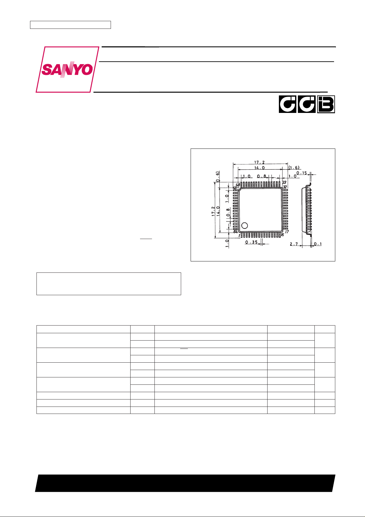
Package Dimensions
unit: mm
3159-QFP64E
CMOS LSI
Ordering number : EN5606
3398HA (OT) No. 5606-1/13
SANYO Electric Co.,Ltd. Semiconductor Bussiness Headquarters
TOKYO OFFICE Tokyo Bldg., 1-10, 1 Chome, Ueno, Taito-ku, TOKYO, 110-8534 JAPAN
1/4 to 1/11 Duty Dynamic Drive VFD Driver
LC75725E
SANYO: QIP64E
[LC75725E]
• CCB is a trademark of SANYO ELECTRIC CO., LTD.
• CCB is SANYO’s original bus format and all the bus
addresses are controlled by SANYO.
Parameter Symbol Conditions Ratings Unit
Maximum supply voltage
V
DD
max V
DD
–0.3 to +6.5
V
V
FL
max V
FL
VDD– 47 to VDD+0.3
Input voltage
V
IN
1 DI, CL, CE, BLK –0.3 to +6.5
V
V
IN
2 OSCI –0.3 to V
DD
+0.3
Output voltage
V
OUT
1 S1 to S43, G1 to G11 V
DD
– 47 to VDD+0.3
V
V
OUT
2 OSCO –0.3 to V
DD
+0.3
Output current
I
OUT
1 S1 to S43 10
mA
I
OUT
2 G1 to G11 30
Allowable power dissipation Pd max Ta = 85°C 300 mW
Operating temperature Topr –40 to +85 °C
Storage temperature Tstg –50 to +150 °C
Specifications
Absolute Maximum Ratings at Ta = 25°C, VSS= 0 V
No. 5606-2/13
LC75725E
Parameter Symbol Conditions
Ratings
Unit
min typ max
Supply voltage
V
DDVDD
4.5 5.0 5.5
V
V
FL
V
FL
VDD– 45 V
DD
Input high-level voltage
V
IH
1 DI, CL, CE, BLK 0.8 V
DD
5.5
V
V
IH
2 OSCI 0.8 V
DD
V
DD
Input low-level voltage V
IL
DI, CL, CE, BLK, OSCI 0 0.2 V
DD
V
Guaranteed oscillator range f
OSC
OSCI, OSCO 1.8 3.7 4.9 MHz
Recommended external resistance R
OSC
OSCI, OSCO 1.0 5.6 22 KΩ
Recommended external capacitance C
OSC
OSCI, OSCO 10 22 47 pF
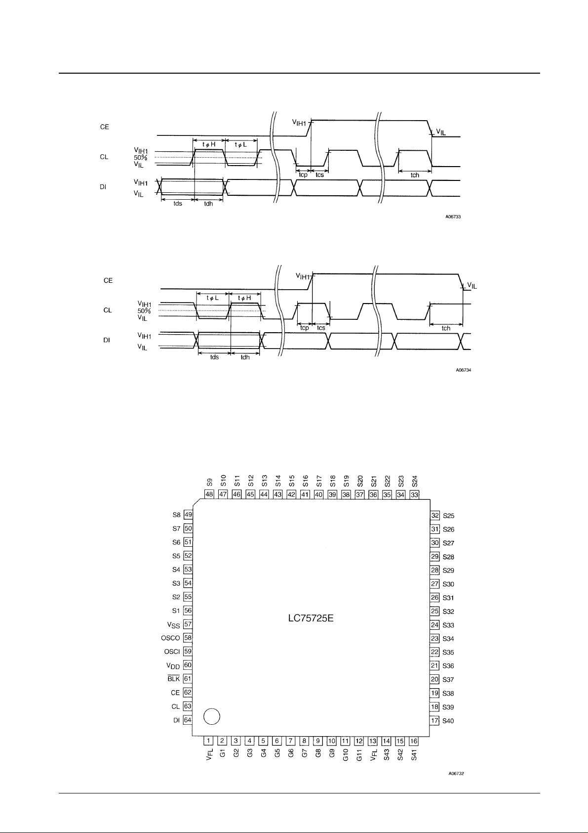
Low level clock pulse width t
øL
CL Figure 1 0.5 µs
High level clock pulse width t
øH
CL Figure 1 0.5 µs
Data setup time t
ds
DI, CL Figure 1 0.5 µs
Data hold time t
dh
DI, CL Figure 1 0.5 µs
CE wait time t
cp
CE, CL Figure 1 0.5 µs
CE setup time t
cs
CE, CL Figure 1 0.5 µs
CE hold time t
ch
CE, CL Figure 1 0.5 µs
BLK switching time t
c
BLK, CE Figure 3 10 µs
Allowable Operating Ranges at Ta = –40 to +85°C, VDD= 4.5 to 5.5 V, VSS= 0 V
Parameter Symbol Conditions
Ratings
Unit
min typ max
Input high-level current
I
IH
1 DI, CL, CE, BLK:V
I
= 5.5 V 5
µA
I
IH
2 OSCI:V
I
= V
DD
5
Input low-level current I
IL
DI, CL, CE, BLK: VI= 0 V –5 µA
V
OH
1 S1 to S43: I
O
= 5 mA VDD– 2.0
Output high-level voltage V
OH
2 G1 to G11: I
O
= 20 mA VDD– 2.0 V
V
OH
3 OSCO: I
O
= 0.5 mA VDD– 2.0
Output low-level voltage V
OL
OSCO: IO= –0.5 mA 2.0 V
Output off voltage V
OFF
S1 to S43, G1 to G11: VFL= VDD– 45 V,
V
DD
– 44 V
Outputs off
Pull-down resistors R
PD
S1 to S43, G1 to G11: VFL= VDD– 45 V,
50 100 200 kΩ
V
O
= V
DD
Oscillator frequency f
OSC
OSCI, OSCO: R
OSC
= 5.6 kΩ, C
OSC
= 22 pF 3.7 MHz
Hysteresis voltage V
H
DI, CL, CE, BLK 0.1 V
DD
V
Current drain I
DD
VDD: Outputs open. Display off,
5 mA
f
OSC
= 3.7 MHz, VFL= VDD– 45 V
Electrical Characteristics in the Allowable Operating Ranges
No. 5606-3/13
LC75725E
1. When CL is stopped at the low level
2. When CL is stopped at the high level
Pin Assignment
Figure 1
Top view
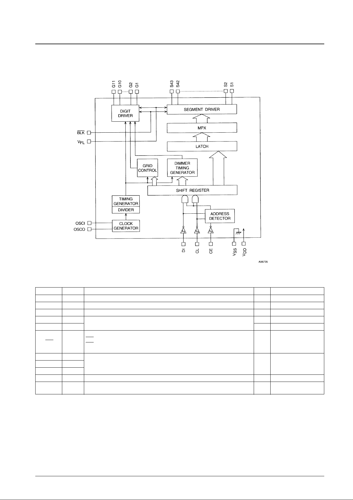
Block Diagram
No. 5606-4/13
LC75725E
Pin Functions
Pin Pin No. Function I/O Handling when unused
V
FL
1, 13 Driver block power supply connection. (Both pins must be connected.) — —
V
DD
60 Logic block power supply connection. Provide a voltage between 4.5 and 5.5 V. — —
V
SS
57 Power supply connection. Connect to the ground. — —
OSCI 59
Oscillator connection. An oscillator circuit is formed by connecting an external resistor
I GND
OSCO 58
and capacitor to these pins.
O OPEN
Display off control input.
BLK 61
BLK = Low (V
SS
) ... Display off. (S1 to S43 and G1 to G11 at VFLlevel.)
I GND
BLK = High (V
DD
) ... Display on.
Note that serial data can be transferred while the display is turned off.
CL 63
DI 64 I GND
CE 62
G1 to G11 2 to 12 Digit outputs. These pins are P-channel open drain outputs with pull-down resistors. O OPEN
S1 to S43 56 to 14
Segment outputs for displaying the display data transferred by serial data input. These pins
O OPEN
are P-channel open drain outputs with pull-down resistors.
Serial data transfer inputs. These pins must be connected to the system microcontroller.
CL: Synchronization clock
DI: Transfer data
CE: Chip enable
 Loading...