

Ordering number : EN6037
40299RM (OT) No. 6037-1/8
Overview
The LC72723 is an RDS (Radio Data System) signal
demodulation IC. This IC integrates a bandpass filter, the
demodulation circuit, and buffer RAM on a single chip
and can read out RDS data in slave mode operation with
the provision of an external clock input. It also supports
master mode, in which the data is read out in
synchronization with an RDS clock output provided by the
IC itself.
Functions
• Bandpass filter: Switched capacitor filter (SCF)
• RDS demodulation: Functions include 57kHz carrier
regeneration, clock regeneration, biphase decoding, and
differential decoding
• Buffer RAM: Stores 128 bits (about 100 ms) of data.
• Data output: Output can be switched between master
mode and slave mode readout.
• RDS ID detection: Supports ID reset
• Standby control: Stops the crystal oscillator.
• Fully adjustment free.
Ratings
• Operating supply voltage: 4.5 to 5.5 V
• Operating temperature: –40 to 85°C
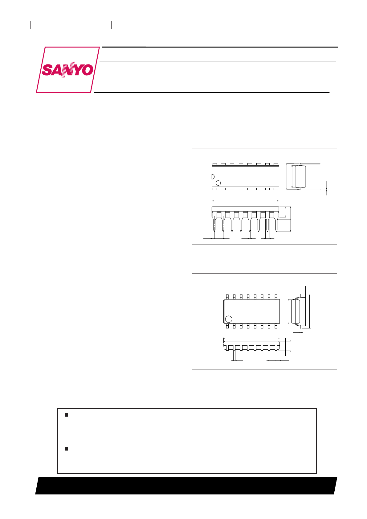
• Packages: DIP16 and MFP16
Package Dimensions
unit: mm
3006B-DIP16
unit: mm
3035A-MFP16
LC72723, LC72723M
SANYO Electric Co.,Ltd. Semiconductor Company
TOKYO OFFICE Tokyo Bldg., 1-10, 1 Chome, Ueno, Taito-ku, TOKYO, 110-8534 JAPAN
RDS Demodulation IC
CMOS IC
Any and all SANYO products described or contained herein do not have specifications that can handle
applications that require extremely high levels of reliability, such as life-support systems, aircraft’s
control systems, or other applications whose failure can be reasonably expected to result in serious
physical and/or material damage. Consult with your SANYO representative nearest you before using
any SANYO products described or contained herein in such applications.
SANYO assumes no responsibility for equipment failures that result from using products at values that
exceed, even momentarily, rated values (such as maximum ratings, operating condition ranges, or other
parameters) listed in products specifications of any and all SANYO products described or contained
herein.
SANYO: DIP16
[LC72723]
1
16
8
9
10.1
0.15
0.6051.27
0.35
0.1
1.8max
1.5
0.625
4.4
5.15
6.4
SANYO: MFP16
[LC72723M]
16
1
19.2
0.71 2.54
0.48
9
6.4
7.62
8
3.0
3.65max
3.4
1.2
0.25

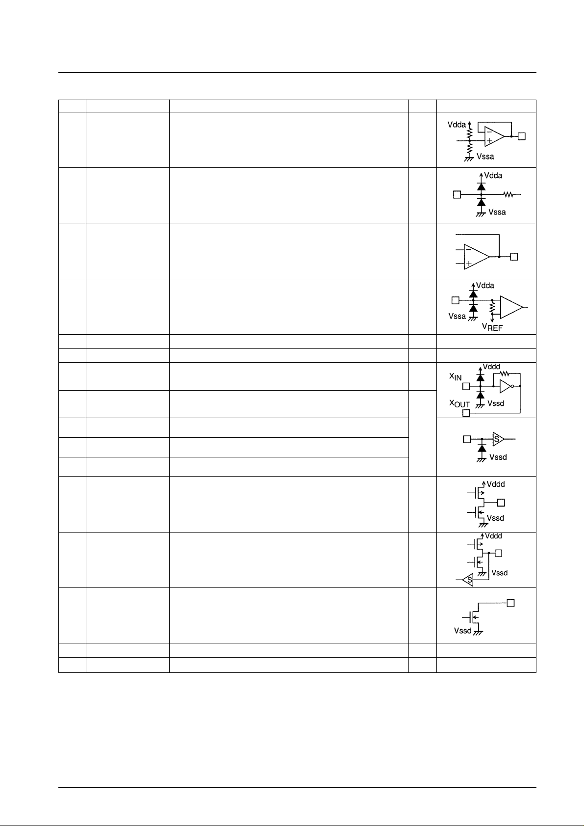
Pin Assignment (DIP16/MFP16)
No. 6037-2/8
LC72723, LC72723M
Block Diagram
No. 6037-3/8
LC72723, LC72723M
Pin Descriptions
Pin No. Pin Function I/O Pin circuit type
Reference voltage output (Vdda/2) Output1 VREF
Base band (multiplex) signal input Input2 MPXIN
Subcarrier output (filter output) Output5 FLOUT
Subcarrier input (comparator input) Input6 CIN
Analog system power supply (+5 V) — —3 Vdda
Analog system ground — —4 Vssa
Crystal element output (4.332 MHz) Output8 XOUT
RDS data output Output14 RDDA
RDS clock output (master mode)
RDS clock input (slave mode)
I/O15 RDCL
RDS ID/ready output (Active low) Output
—
—
—
—
16 RDS-ID/READY
Digital system power supply (+5 V)11 Vddd
Digital system ground10 Vssd
Test input7 TEST
Crystal element input (or external reference signal input)
Input
9 XIN
Readout mode setting (0: master, 1: slave)12 MODE
RDS ID and RAM reset (Active high logic)13 RST
 Loading...