

Ordering number : ENN6123A
51202AS (OT)/83199TH (OT) No. 6123-1/15
Overview
The LC72722 and LC72722M, LC72722PM are singlechip system ICs that implement the signal processing
required by the European Broadcasting Union RDS (Radio
Data System) standard and by the US NRSC (National
Radio System Committee) RDBS (Radio Broadcast Data
System) standard. These ICs include band-pass filter,
demodulator, synchronization, and error correction circuits
as well as data buffer RAM on chip and perform effective
error correction using a soft-decision error correction
technique.
Functions
• Band-pass filter: Switched capacitor filter (SCF)
• Demodulator: RDS data clock regeneration and
demodulated data reliability information
• Synchronization: Block synchronization detection (with
variable backward and forward protection conditions)
• Error correction: Soft-decision/hard-decision error
correction
• Buffer RAM: Adequate for 24 blocks of data (about 500
ms) and flag memory
• Data I/O: CCB interface (power on reset)
Features
• Error correction capability improved by soft-decision
error correction
• The load on the control microprocessor can be reduced
by storing decoded data in the on-chip data buffer RAM.
• Two synchronization detection circuits provide
continuous and stable detection of the synchronization
timing.
• Data can be read out starting with the backwardprotection block data after a synchronization reset.
• Bit slip detection and correction
• Low spurious radiation
• Fully adjustment free
• Operating power-supply voltage: 4.5 to 5.5 V
• Operating temperature: –40 to +85°C
• Package: LC72722 : DIP24S
LC72722M : MFP24S
LC72722PM : MFP24
Package Dimensions
unit: mm
3067A-DIP24S
LC72722, 72722M, 72722PM
SANYO Electric Co.,Ltd. Semiconductor Company
TOKYO OFFICE Tokyo Bldg., 1-10, 1 Chome, Ueno, Taito-ku, TOKYO, 110-8534 JAPAN
Single-Chip RDS
Signal-Processing System LSI
CMOS IC
Any and all SANYO products described or contained herein do not have specifications that can handle
applications that require extremely high levels of reliability, such as life-support systems, aircraft’s
control systems, or other applications whose failure can be reasonably expected to result in serious
physical and/or material damage. Consult with your SANYO representative nearest you before using
any SANYO products described or contained herein in such applications.
SANYO assumes no responsibility for equipment failures that result from using products at values that
exceed, even momentarily, rated values (such as maximum ratings, operating condition ranges, or other
parameters) listed in products specifications of any and all SANYO products described or contained
herein.
• CCB is a trademark of SANYO ELECTRIC CO., LTD.
• CCB is SANYO’s original bus format and all the bus
addresses are controlled by SANYO.
0.48
(3.25)
3.3
3.9max
0.51min
21.0
(0.71)
1.78
0.25
7.62
6.4
1
12
24
13
0.95
0.9
SANYO: DIP24S
[LC72722]
unit: mm
3112A-MFP24S
unit: mm
3045C-MFP24
No. 5602-2/15
LC72722, 72722M, 72722PM
1
12
24 13
1.27
15.2
0.35
10.5
7.9
(0.62)
2.35max
0.1
(2.15)
0.65
0.15
SANYO: MFP24
[LC72722PM]
1 12
24
13
12.5
(0.75)
1.0
0.15
0.35
5.4
7.6
0.63
1.7max
1.5
0.1
SANYO: MFP24S
[LC72722M]
Pin Assignment
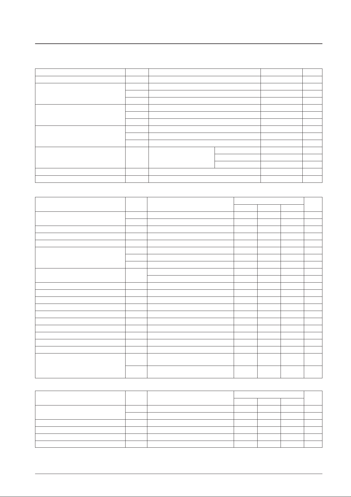
Block Diagram
A12363
1 24V
REF
SYR
2 23MPXIN CE
3 22Vdda DI
4 21Vssa CL
5 20FLOUT DO
6 19CIN
LC72722
LC72722M
LC72722PM
Top view
RDS-ID
7 18T1 SYNC
8 17T2 T7(CORREC/ARI-ID/TA/BEO)
9 16T3(RDCL) T6(ERROR/57K/TP/BE1)
10 15T4(RDDA) Vssd
11 14T5(RSFT) Vddd
12 13X
OUT
X
IN
REFERENCE
VOLTAGE
ANTIALIASING
FILTER
SMOOTHING
FILTER
57 kHz
BPF
(SCF)
TEST
+
–
PLL
(57 kHz)
V
REF
CLOCK
RECOVERY
(1187.5 Hz)
DATA
DECODER
SYNC
DETECT-2
SYNC
DETECT-1
OSC/DIVIDER
MEMORY CONTROL
CLK(4.332 MHz)
+5V +5V
Vdda
Vssa
MPXIN
T2
T3 to T7
T1
CCB
DI
CE
CL
RAM
(24 BLOCK DATA)
ERROR CORRECTION
(SOFT DECISION)
SYNC/EC CONTROLLER
DO
X
IN
X
OUT
SYR
SYNC
RDS-ID
Vssd
Vddd
CINFLOUT
V
REF
A12364
No. 5602-3/15
LC72722, 72722M, 72722PM
Pin Functions
Pin No. Pin name Function I/O Pin circuit
1 VREF Reference voltage output (Vdda/2) Output
2 MPXIN Baseband (multiplexed) signal input Input
5 FLOUT Subcarrier output (filter output) Output
6 CIN Subcarrier input (comparator input) Input
3 Vdda Analog system power supply (+5 V) — —
4 Vssa Analog system ground — —
12 XOUT Crystal oscillator output (4.332/8.664 MHz) Output
13 XIN Crystal oscillator input (external reference signal input)
7 T1 Test input (This pin must always be connected to ground.) Input
8 T2
Test input (standby control)
0: Normal operation, 1: Standby state (crystal oscillator stopped)
9 T3 (RDCL) Test I/O (RDS clock output)
10 T4 (RDDA) Test I/O (RDS data output)
11 T5 (RSFT) Test I/O (soft-decision control data output)
16 T6 (ERROR/57K/TP/BE1)
Test I/O (error status output, regenerated carrier output,
I/O*
TP output, error block count output)
17 T7 (CORREC/ARI-ID/TA/BE0)
Test I/O (Error correction status output, SK detection output,
TA output, error block count output)
18 SYNC Block synchronization detection output
19 RDS-ID RDS detection output
Output
20 DO Data output
21 CL Clock input
22 DI Data input
Input
23 CE Chip enable
24 SYR Synchronization and RAM address reset (active high)
14 Vddd Digital system power supply (+5 V) — —
15 Vssd Digital system ground — —
Note: * Normally function as an output pin. Used as an I/O pin in test mode, which is not available to user applications.
Serial data interface (CCB)
Vdda
Vssa
A12365
Vdda
Vssa
A12366
A12367
–
+
Vdda
V
REF
Vssa
A12368
Vddd
Vssd
A12369
X
OUT
X
IN
A12370
Vssd
S
A12371
Vssd
A12372
Vssd
A12373
Vssd
S
No. 5602-4/15
LC72722, 72722M, 72722PM
Parameter Symbol Conditions Ratings Unit
Maximum supply voltage V
DD
max Vddd, Vdda: Vdda ≤ Vddd +0.3 V –0.3 to +7.0 V
V
IN
1 max CL, DI, CE, SYR, T1, T2, T3, T4, T5, T6, T7, SYNC –0.3 to +7.0 V
Maximum input voltage V
IN
2 max XIN –0.3 to Vddd +0.3 V
V
IN
3 max MPXIN, CIN –0.3 to Vdda +0.3 V
V
O
1 max DO, SYNC, RDS-ID, T3, T4, T5, T6, T7 –0.3 to +7.0 V
Maximum output voltage V
O
2 max XOUT –0.3 to Vddd +0.3 V
V
O
3 max FLOUT –0.3 to Vdda +0.3 V
I
O
1 max DO, T3, T4, T5, T6, T7 6.0 mA
Maximum output current I
O
2 max XOUT, FLOUT 3.0 mA
I
O
3 max SYNC, RDS-ID 20.0 mA
LC72722:DIP24S: 350 mW
Allowable power dissipation Pd max Ta ≤ 85°C LC72722M:MFP24S: 150 mW
LC72722PM:MFP24: 175 mW
Operating temperature Topr –40 to +85 °C
Storage temperature Tstg –55 to +125 °C
Specifications
Absolute Maximum Ratings at Ta = 25°C, Vssd = Vssa = 0 V
Parameter Symbol Conditions
Ratings
Unit
min typ max
Supply voltage
V
DD
1 Vddd, Vdda: Vddd = Vdda 4.5 5.0 5.5 V
V
DD
2 Vddd: Serial data hold voltage 2.0 V
Input high-level voltage V
IH
CL, DI, CE, SYR, T1, T2 0.7 Vddd 6.5 V
Input low-level voltage V
IL
CL, DI, CE, SYR, T1, T2 0 0.3 Vddd V
Output voltage V
O
DO, SYNC, RDS-ID, T3, T4, T5, T6, T7 6.5 V
V
IN
1 MPXIN : f = 57 ±2 kHz 50 mVrms
Input amplitude V
IN
2 MPXIN : 100% modulation composite 100 mVrms
V
XIN
XIN 400 1500 mVrms
Guaranteed crystal oscillator frequencies Xtal
XIN, XOUT : CI ≤ 120 Ω (XS = 0) 4.332 MHz
XIN, XOUT : CI ≤ 70 Ω (XS = 1) 8.664 MHz
Crystal oscillator frequency deviation TXtal XIN, XOUT : f
O
= 4.322 MHz, 8.664 MHz ±100 ppm
Data setup time t
SU
DI, CL 0.75 µs
Data hold time t
HD
DI, CL 0.75 µs
Clock low-level time t
CL
CL 0.75 µs
Clock high-level time t
CH
CL 0.75 µs
CE wait time t
EL
CE, CL 0.75 µs
CE setup time t
ES
CE, CL 0.75 µs
CE hold time t
EH
CE, CL 0.75 µs
CE high-level time t
CE
CE 20 ms
Data latch change time t
LC
1.15 µs
t
DC
DO, CL: Differs depending on the value of the
0.46 µs
Data output time
pull-up resistor used.
t
DH
DO, CE: Differs depending on the value of the
0.46 µs
Allowable Operating Ranges at Ta = –40 to +85°C, Vssd = Vssa = 0 V
Parameter Symbol Conditions
Ratings
Unit
min typ max
Input resistance
Rmpxin MPXIN–Vssa : f = 57 kHz 43 kΩ
Rcin CIN–Vssa : f = 57 kHz 100 kΩ
Internal feedback resistance Rf XIN 1.0 MΩ
Center frequency fc FLOUT 56.5 57.0 57.5 kHz
–3 dB bandwidth BW – 3 dB FLOUT 2.5 3.0 3.5 kHz
Gain Gain MPXIN–FLOOUT : f = 57 kHz 28 31 34 dB
Electrical Characteristics at Ta = –40 to +85°C, Vssd = Vssa = 0 V
Continued on next page.
No. 5602-5/15
LC72722, 72722M, 72722PM
Parameter Symbol Conditions
Ratings
Unit
min typ max
Att1 FLOUT : ∆f = ±7 kHz 30 dB
Stop band attenuation Att2 FLOUT : f < 45 kHz, f > 70 kHz 40 dB
Att3 FLOUT : f < 20 kHz 50 dB
pull-up resistor used.Reference voltage output Vref VREF : Vdda = 5 V 2.5 V
Hysteresis V
HIS
CL, DI, CE, SYR, T1, T2 0.1 Vddd V
Output low-level voltage
V
OL
1 DO, T3, T4, T5, T6, T7 : I = 2 mA 0.4 V
V
OL
2 SYNC, RDS-ID : I = 8 mA 0.4 V
Input high-level current
I
IH
1 CL, DI, CE, SYR, T1, T2 : VI= 6.5 V 5.0 µA
I
IH
2 XIN : VI= Vddd 2.0 11 µA
Input low-level current
I
IL
1 CL, DI, CE, SYR, T1, T2 : VI= 0 V 5.0 µA
I
IL
2 XIN : VI= 0 V 2.0 11 µA
Output off leakage current I
OFF
DO, SYNC, RDS-ID, T3, T4, T5, T6, T7 :
5.0 µA
V
O
= 6.5 V
Current drain Idd Vddd + Vdda 9 mA
Continued from preceding page.
CCB Output Data Format
• Each block of output data consists of 32 bits (4 bytes), of which 2 bytes are RDS data and 2 bytes are flag data.
• Any number of 32-bit output data blocks can be output consecutively.
• When there is no data that can be read out in the internal memory, the system outputs blocks of all-zero data
consecutively.
• If data readout is interrupted, the next read operation starts with the 32-bit data block whose readout was interrupted.
However, if only the last bit remains to be read, it will not be possible to reread that whole block.
• The check bits (10 bits) are not output.
• The data valid/invalid decision is made by referencing the error information flags (E0 to E2) must not be referred to.
• When the first leading bits are not "1010", the read in data is invalid, and the read operation is cancelled.
1. Offset word detection flag (1 bit): OWD
OWD Offset word detection
1 Detected
0 Not detected (protection function operating)
CCB address 6C
Output data/first bit
Last bit
(8) RDS data
(7) Error information flags
(6) Synchronization established flag
(5) ARI (SK) detection flag
(4) RAM data remaining flag
(3) Consecutive RAM read out possible flag
(2) Offset word information flag
(1) Offset word detection flag
Fixed pattern (1010)
B
B1B2B3A0A1A2A
DI
0
0
0 1 1 0 1 1 0
3
O
B
DO
1 0 1 0
B1B0R
W
2
D
E
R
R
A
S
F
F
1
0
E2E1E
R
Y
I
C
D
D
D
D
D
D
1
1
1
0
5
1
4
3
2
D9D8D7D6D5D4D3D2D1D
1
1
1
0
0

No. 5602-6/15
LC72722, 72722M, 72722PM
2. Offset word information flag (3 bits): B0 to B2
B B B
Offset word
2 1 0
0 0 0 A
0 0 1 B
0 1 0 C
0 1 1 C’
1 0 0 D
1 0 1 E
1 1 0 Unused
1 1 1 Unused
3. Consecutive RAM readout possible flag (1 bit): RE
RE RAM data information
1 The next data to be read out is in RAM.
0 This data item is the last item in RAM, and the next data is not present.
ARI SK signal
1 Detected
0 Not detected
4. RAM data remaining flag (2 bits): RF0, RF1
Caution: This value is only meaningful when RE is 1. When RE is 0, there is no data in RAM, even if RF is 00.
If a synchronization reset was applied using SYR, then the backward protection block data that was written to memory is also counted in this
value.
Caution: This flag indicates the synchronization state of the circuit at the point where the data block being output was received.
On the other hand, the SYNC pin (pin 18) output indicates the current synchronization state of the circuit.
Caution: If the number of errors exceeds the value of the EC0 to EC2 setting (see the section on the CCB input format), the error information flags will be
set to the “Correction not possible” value.
When the error flags E0 to E2 are 011 (indicating that correction is not possible) the data must be handled as invalid data.
RF1 RF0 Remaining data in RAM (number of blocks)
0 0 1 to 7
0 1 8 to 15
1 0 16 to 23
1 1 24
5. ARI (SK) detection flag (1 bit): ARI
SYC Synchronization detection
1 Synchronized
0 Not synchronized
6. Synchronization established flag (1 bit): SYC
7. Error information flags (3 bits): E0 to E2
8. RDS data (16 bits): D0 to D15
This data is output with the MSB first and the LSB last.
Caution: When error correction was not possible, the input data is output without change.
E E E Number of
2 1 0 bits corrected
0 0 0 0 (no errors)
0 0 1 1
0 1 0 2
0 1 1 3
1 0 0 4
1 0 1 5
1 1 0 Correction not possible
1 1 1 Unused

No. 5602-7/15
LC72722, 72722M, 72722PM
CCB Input Data Format
Caution: The bits labeled with an asterisk must be set to 0.
1. Synchronization protection (forward protection) method setting (4 bits): FS0 to FS3
FS3 = 0: If offset words in the correct order could not be detected continuously during the number of blocks specified
by FS0 to FS2, take that to be a lost synchronization state.
FS3 = 1: If blocks with uncorrectable errors were received consecutively during the number of blocks specified by
FS0 to FS2, take that to be a lost synchronization state.
Initial value: FS0 = 0, FS1 = 1, FS2 = 0, FS3 = 0
Initial value: BS = 0
F F F
S S S Condition for detecting lost synchronization
0 1 2
0 0 0 If 3 consecutive blocks matching the FS3 condition are received.
1 0 0 If 4 consecutive blocks matching the FS3 condition are received.
0 1 0 If 5 consecutive blocks matching the FS3 condition are received.
1 1 0 If 6 consecutive blocks matching the FS3 condition are received.
0 0 1 If 8 consecutive blocks matching the FS3 condition are received.
1 0 1 If 10 consecutive blocks matching the FS3 condition are received.
0 1 1 If 12 consecutive blocks matching the FS3 condition are received.
1 1 1 If 16 consecutive blocks matching the FS3 condition are received.
2. Synchronization detection method setting (1 bit): BS
BS Synchronization detection conditions
0 If, during 3 blocks, 2 blocks of offset words were detected in the correct order.
1 If the offset words were detected in the correct order in 2 consecutive blocks.
[1] CCB address 6A
[2] CCB address 6B
IN1 data, first bit
IN2 data, first bit
(12) Circuit control
(5) Error correction method setting
(4) RAM write control
(3) Synchronization and RAM address reset
(2) Synchronization detection method setting
(1) Synchronization protection method setting
(11) Test mode settings
(10) Output pin settings
(9) RDS/RBDS selection
(8) Demodulation circuit phase control
(7) Crystal oscillator frequency selection
(6) Intermittent DO output setting
(12) Circuit control
DI
B
0
1 1 0 1 0 1 1 0
B1B2B3A0A1A2A
3
C
T
1
S
P
0
S
P
1
P
T
0
T
S
0
T
S
1
T
S
2
T
S
3
P
T
1
P
T
2
X
S
P
L
0
P
L
1
* *
R
M
B
B1B2B3A0A1A2A
0
DI
0 1 0 1 0 1 1 0
S
F
F
F
3
F
S
S
S
S
0
1
2
3
O
E
E
B
Y
* * *
S
R
E
W
C
C
C
E
0
1
2
E
E
C
C
C
T
3
4
0

No. 5602-8/15
LC72722, 72722M, 72722PM
3. Synchronization and RAM address reset (1 bit): SYR
Initial value: SYR =0
Caution: 1. To apply a synchronization reset, set SYR to 1 temporarily using the CCB, and then set it back to 0 again using the CCB.
The circuit will start synchronization capture operation at the point SYR is set to 0.
2. The SYR pin (pin 24) also provides an identical reset control operation. Applications can use either method. However, the control method
that is not used must be set to 0 at all times. Any pulse with a width of over 250 ns will suffice.
3. A reset must be applied immediately after the reception channel is changed. If a reset is not applied, reception data from the previous
channel may remain in memory.
4. Data read out after a synchronization reset is read out starting with the backward protection block data preceding the establishment of
synchronization.
SYR Synchronization detection circuit RAM
0 Normal operation (reset cleared) Normal write (See the description of the OWE bit.)
1 Forced to the unsynchronized state (synchronization reset)
After the reset is cleared, start writing from the data prior to the
establishment of synchronization, i.e. the data in backward protection.
Initial value: OWE = 0
Initial values: EC0 = 0, EC1 = 1, EC2 = 0, EC3 = 0, EC4 = 1
Caution: 1. If soft-decision A or soft-decision B is specified, soft-decision control will be performed even if the number of bits corrected is set to 0 (error
detection only). With these settings, data will be output for blocks with no errors.
2.As opposed to soft-decision B, the soft-decision A setting suppresses soft decision error correction.
4. RAM write control (1 bit): OWE
5. Error correction method setting (5 bits): EC0 to EC4
OWE RAM write conditions
0 Only data for which synchronization had been established is written.
1 Data for which synchronization not has been established (unsynchronized data) is also written. (However, this applies when SYR = 0.)
E E E
Number of
C C C
bits corrected
0 1 2
0 0 0 0 (error detection only)
1 0 0 1 or fewer bits
0 1 0 2 or fewer bits
1 1 0 3 or fewer bits
0 0 1 4 or fewer bits
1 0 1 5 or fewer bits
0 1 1 Illegal value
1 1 1 Illegal value
E E
C C Soft-decision setting
3 4
0 0 Mode 0: Hard decision
1 0 Mode 1: Soft decision A
0 1 Mode 2: Soft decision B
1 1 Illegal value
6. Intermittent DO output setting
SP0 SP1 DO output state
0 0 DO goes low when one or more blocks of data are written to memory.
1 0 DO goes low when 4 or more blocks of data are written to memory.
0 1 DO goes low when 8 or more blocks of data are written to memory.
1 1 DO goes low when 12 or more blocks of data are written to memory.
7. Crystal oscillator frequency selection (1 bit): XS
XS = 0: 4.332 MHz
XS = 1: 8.664 MHz
Initial value: XS = 0
Initial values: SP0 = 0, SP1 = 0

No. 5602-9/15
LC72722, 72722M, 72722PM
8. Demodulation circuit phase control (2 bits): PL0, PL1
Initial values: PL0 = 0, PL1 = 1
Caution: 1. When PL0 is 0 (normal operation), the IC detects the presence or absence of the ARI signal and reproduces the RDS data by automatically
controlling the demodulation phase with respect to the reproduced carrier. However, the initial phase following a synchronization reset is set
by PL1.
2.If PL0 is set to 1, the demodulation circuit phase is locked according to the PL1 setting at either 90° (PL1 = 0) or 0° (PL1 = 1), allowing RDS
data to be reproduced. When ARI is not present, PL1 should be set to 0, since the RDS data is reproduced by detecting at a phase of 90°
with respect to the reproduced carrier. When ARI is present, PL1 should be set to 1, since detection is at 0°. In cases where the ARI
presence is known in advance, more stable reproduction can be achieved by fixing the demodulation phase in this manner.
PL0 PL1 Demodulation circuit phase control
0 0/1 <Normal operation> when ARI presence or absence is unclear.
1
0 If the circuit determines that the ARI signal is absent: 90° phase
1 If the circuit determines that the ARI signal is present: 0° phase
9. RDS/RBDS (MMBS) selection (1 bit): RM
Initial value: RM = 0
—: Open,
●●, ●: Output enabled (● = reverse polarity)
Initial values: PT0 = 1, PT1 = 1, PT2 = 0 (mode 3)
Caution: 1. When PT2 is set to 1, T6 (ERROR/57K/TP), T7 (CORREC/ARI-ID/TA) SYNC, and RDS-ID pins change to active high.
2.The output pins (T3 to T7, SYNC, and RDS-ID) are all open-drain pins, and require external pull-up resistors to output data.
TP = Traffic program code
RM RBDS support Decoding method
0 None Only RDS data is decoded correctly (Offset word E is not detected.)
1 Provided RDS and MMBS data is decoded correctly (Offset word E is also detected.)
10. Output pin settings (3 bits): PT0 to PT2
These bits control the T3, T4, T5, T6, T7, SYNC, and RDS-ID pins.
P P P
T3 T4 T5 T6 T7
Mode T T T
0 1 2 RDCL RDDA RSFT ERROR 57K TP BE1 CORREC ARI-ID TA BE0
0 0 0 0 — — — — — — — — — — —
1 1 0 0 — — — — — ●● — — — ●● —
2 0 1 0 ●● ●● ●● — ●● — — — ●● — —
3 1 1 0 ●● ●● ●● ●● — — — ●● — — —
4 0 0 1 — — — — — — ●● — — — ●●
5 1 0 1 — — — — — ● — — — ● —
6 0 1 1 ●● ●● ●● — ● — — — ● — —
7 1 1 1 ●● ●● ●● ● — — — ● — — —
Mode 1 (PT2 = 0) Pin T6 (TP)
TP = 0 detected High (1)
TP = 1 detected Low (0)
TA = Traffic announcement code
Mode 1 (PT2 = 0) Pin T7 (TA)
TA = 0 detected High (1)
TA = 1 detected Low (0)
Mode 2 (PT2 = 0) Pin T7 (ARI-ID)
No SK High (1)
SK present Low (0)
Mode 3 (PT2 = 0) Pin T6 (ERROR) Pin T7 (CORREC)
Correction not possible Low (0) Low (0)
Errors corrected High (1) Low (0)
No errors High (1) High (1)

No. 5602-10/15
LC72722, 72722M, 72722PM
These pins indicate the number of blocks in a set of 48 blocks that had errors before correction. The output polarity of these pins is fixed at the values
listed in the table.
Mode 4
Pin T6 (BE1) Pin T7 (BE0)
Number of error blocks (B)
B = 0 Low (0) Low (0)
1 ≤ B ≤ 20 Low (0) High (1)
20 < B ≤ 40 High (1) Low (0)
40 < B ≤ 48 High (1) High (1)
Caution: The output indicates the synchronization state for the previous block.
Mode (PT2 = 0) The SYNC pin
0 to 2 When synchronized: Low (0). When unsynchronized: High (1)
When synchronized: Goes high for a fixed period (421 µs) at
3 the start of a block and then goes low.
When unsynchronized: High (1)
When PT2 = 0 The RDS-ID pin
No RDS High (1)
RDS present Low (0)
11. Test mode settings (4 bits): TS0 to TS3
Initial values: TS0 = 0, TS1 = 0, TS2 = 0, TS3 = 0
(Applications must set these bits to the above values.)
Notes: The T1 and T2 pins (pins 7 and 8) are related to test mode as follows:
The T1 pin must be tied to VSS(0 V).
Initial values: CT0 = 0, CT1 = 0
Pin T1 Pin T2 LSI operation Notes
0 0 Normal operating mode
These states are user settable
0 1 Standby mode (crystal oscillator stopped)
1 0/1 LSI test mode Users cannot use this state
12. Circuit control (2 bits): CT0 and CT1
Item Control
CT0 RSFT control When set to 1, soft-decision control data (RSFT) is more difficult to generate.
CT1 RDS-ID detection condition When set to 1, the RDS-ID detection conditions are made more restrictive.
RDCL/RDDA/RSFT and ERROR/CORREC/SYNC Output Timing
Timing 1
17 µs
421 µs 421 µs
Tp2
Tp1
17 µs
RDCL output
RSFT output
RDDA output
A12377

No. 5602-11/15
LC72722, 72722M, 72722PM
Timing 2 (mode 3, PT2 = 0)
A12378
Input data
Error correction
SYNC output
ERROR output
CORREC output
Sync NG Sync OK Sync OK Sync OK Sync OK Sync OK Sync NG Sync NG
Data
correctedNoerrorsNoerrors
Data
corrected
Uncorrectable Uncorrectable
Tp1 Tp1
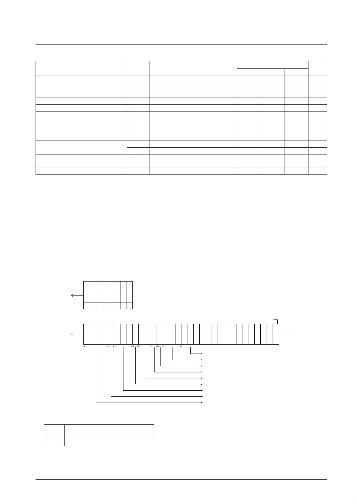
Serial Data Input and Output Methods
Data is input and output using the CCB (computer control bus), which is the Sanyo audio IC serial bus format. This IC
adopts an 8-bit address CCB format.
I/O mode
(LSB) Address (MSB)
Comment
B0 B1 B2 B3 A0 A1 A2 A3
1 IN1 (6A) 0 1 0 1 0 1 1 0
· Control data input mode, also referred to as “serial data input” mode.
· This is a 16-bit data input mode.
2 IN2 (6B) 1 1 0 1 0 1 1 0
· Control data input mode, also referred to as “serial data input” mode.
· This is a 16-bit data input mode.
3 OUT (6C) 0 0 1 1 0 1 1 0
· Data output mode, also referred to as “serial data output” mode.
· The data for multiple blocks can be output sequentially in this mode.
I/O mode determined
For the CL normal high state
For the CL normal low state
CE
CL
DI
DO
1
2
B0 B1 B2 B3 A0 A1 A2 A3
1
2
1
2
First Data IN1/2
First Data OUT
First Data OUT
A12379

No. 5602-12/15
LC72722, 72722M, 72722PM
Serial data input (IN1, IN2) tSU, tHD, tEL, tES, tEH≥ 0.75 µs tLC< 1.15µs tCE< 20 ms
CL: Normal high
CL: Normal low
t
SU
t
HD
t
EL
t
ES
t
EH
t
LC
t
CE
B0 B1 B2 B3 A0 A1 A2 A3
FS0
CT1
FS10FS2
SP0
FS3
SP1
EC3
TS0
EC4
TS1
CT0
TS20TS3
CE
CL
DI
Internal data
A12380
t
SU
t
HD
t
EL
t
ES
t
EH
t
LC
t
CE
B0 B1 B2 B3 A0 A1 A2
A3
FS1
0
FS0
CT1
FS2
SP0
FS3
SP1
EC3
TS0
EC4
TS1
CT0
TS20TS3
CE
CL
DI
Internal data
A12381
Serial data output (OUT) tSU, tHD, tEL, tES, tEH≥ 0.75 µs tDC, tDH< 0.46 µs tCE< 20 ms
CL: Normal high
CL: Normal low
Notes: 1. Since the DO pin is an n-channel open-drain output, the transition times (tDC, tDH) will differ with the value of
the pull-up resistor used.
2. The CE, CL, DI, and DO pins can be connected to the corresponding pins on other ICs that use the CCB
interface. (However, we recommend connecting the DO and CE pins separately if the number of available
microcontroller ports allows it.)
3. Serial data I/O becomes possible after the crystal oscillator starts oscillation.
t
SU
t
HD
t
EL
t
ES
t
EH
t
DC
t
DC
t
CE
B0 B1 B2 B3 A0 A1 A2 A3
1 0 1 0 D3 D2 D1 D0
CE
CL
DI
DO
A12382
t
DH
t
SU
t
HD
t
DC
t
DC
B0 B1 B2 B3 A0 A1 A2 A3
1 0 1 0 D3 D2 D1 D0
CE
CL
DI
DO
A12383
t
DH
t
EL
t
ES
t
EH
t
CE

No. 5602-13/15
LC72722, 72722M, 72722PM
Serial data timing
CL: Normal high
CL: Normal low
Old
New
t
CE
V
IH
V
IL
V
IH
V
IL
t
EH
t
DH
t
LC
t
ES
t
DC
t
EL
t
CL
t
CH
t
SU
t
HD
V
IH
V
IL
V
IH
V
IL
V
IH
V
IL
V
IH
CE
CL
DI
DO
Internal data latch
A12384
t
CE
V
IH
V
IL
V
IL
V
IH
V
IL
t
EH
t
DH
t
LC
t
ES
t
DC
t
DC
t
EL
Old New
t
CL
t
CH
t
SU
t
HD
V
IH
V
IL
V
IH
V
IL
V
IH
V
IL
V
IL
CE
CL
DI
DO
A12385
Internal data latch
Parameter Symbol Conditions
Ratings
Unit
min typ max
Data setup time t
SU
DI, CL 0.75 µs
Data hold time t
HD
DI, CL 0.75 µs
Clock low-level time t
CL
CL 0.75 µs
Clock high-level time t
CH
CL 0.75 µs
CE wait time t
EL
CE, CL 0.75 µs
CE setup time t
ES
CE, CL 0.75 µs
CE hold time t
EH
CE, CL 0.75 µs
CE high-level time t
CE
CE 20 ms
Data latch transition time t
LC
1.15 µs
Data output time
t
DC
DO, CL 0.46 µs
t
DH
DO, CE 0.46 µs
Differs with the value of
the pull-up resistor used.

No. 5602-14/15
LC72722, 72722M, 72722PM
CE pin
DO pin
(Last data)-1 Last data
New data
T
Tdo
DO check (Tdo < T)
A12386
2. When DO goes low 265 µs after data is read out
Here, there is data that has not been read out remaining in the data buffer. In this case, applications are guaranteed to
be able to read out that data without it being overwritten by new data if they start a readout operation within 20 ms of
DO going low. (Note that this is the worst case condition.)
Notes: 1. Although an application can determine whether or not there is data remaining in the buffer by checking the DO
level with the above timing, checking the RE and RF flags in the serial data is a preferable method.
2. Applications are not limited to reading out one block of data at a time, but rather can read out multiple blocks
of data continuously as described above. When using this method, if an application references the RE and RF
flags in the data while reading out data, it can determine the amount of data remaining. However, the length of
the period for data readout (the period the CE pin remains high) must be kept under 20 ms.
3. If the DO pin is shared with other ICs that use the CCB interface, the application must identify which IC
issued the readout request. One method is to read out data from the LC72722 and either check whether
meaningful data has been read (if the LC72722 is not requesting a read, data consisting of all zeros will be read
out) or check whether the DO level goes low within the 256 µs following the completion of the read (if the DO
pin goes low, then the request was from another IC).
CE pin
DO pin
(Last data)-2
(Last data)-1
Last data
T
Tdo
DO check (Tdo < T)
A12387
1. When the DO pin is high following the 265 µs period (Tdo) after data is read out
Here, the buffer is in the empty state, i.e. the state where new data has not been written. After this, when the DO pin
goes low, applications are guaranteed to be able to read out that data without it being overwritten by new data if they
start a readout operation within 480 ms of DO going low.
DO pin operation
This IC incorporates a RAM data buffer that can hold up to 24 blocks of data. At the point where one block of data is
written to this RAM, the IC issues a read request by switching the DO pin from high to low when SP = 00. (See the CCB
input data fromat.)
The DO pin always goes high for a fixed period (Tdo = 265 µ s) after a readout and CE goes low. When all the data in the
data buffer has been read out, the DO pin is held in the high state until a new block of data has been written to the RAM.
(When SP = 00) If there is data that has not yet been read remaining in the data buffer, the DO pin goes low after the Tdo
time has elapsed.
After a synchronization reset, the DO pin is held high until synchronization is established. It goes low at the point where
the IC synchronizes(When SP = 00).

PS No. 5602-15/15
LC72722, 72722M, 72722PM
This catalog provides information as of May, 2002. Specifications and information herein are subject to
change without notice.
Specifications of any and all SANYO products described or contained herein stipulate the performance,
characteristics, and functions of the described products in the independent state, and are not guarantees
of the performance, characteristics, and functions of the described products as mounted in the customer’s
products or equipment. To verify symptoms and states that cannot be evaluated in an independent device,
the customer should always evaluate and test devices mounted in the customer’s products or equipment.
SANYO Electric Co., Ltd. strives to supply high-quality high-reliability products. However, any and all
semiconductor products fail with some probability. It is possible that these probabilistic failures could
give rise to accidents or events that could endanger human lives, that could give rise to smoke or fire,
or that could cause damage to other property. When designing equipment, adopt safety measures so
that these kinds of accidents or events cannot occur. Such measures include but are not limited to protective
circuits and error prevention circuits for safe design, redundant design, and structural design.
In the event that any or all SANYO products (including technical data, services) described or contained
herein are controlled under any of applicable local export control laws and regulations, such products must
not be exported without obtaining the export license from the authorities concerned in accordance with the
above law.
No part of this publication may be reproduced or transmitted in any form or by any means, electronic or
mechanical, including photocopying and recording, or any information storage or retrieval system,
or otherwise, without the prior written permission of SANYO Electric Co., Ltd.
Any and all information described or contained herein are subject to change without notice due to
product/technology improvement, etc. When designing equipment, refer to the “Delivery Specification”
for the SANYO product that you intend to use.
Information (including circuit diagrams and circuit parameters) herein is for example only; it is not
guaranteed for volume production. SANYO believes information herein is accurate and reliable, but
no guarantees are made or implied regarding its use or any infringements of intellectual property rights
or other rights of third parties.
Sample Application Circuit
Notes: 1. Determine the value of the DO pin pull-up resistor based on the required serial data transfer speed.
2. If the SYR pin is unused, it must be connected to ground.
+
1 24
V
REF
SYR
SYR
2 23
MPXIN CE
3 22
Vdda DI
4 21
Vssa CL
5 20
FLOUT DO
6 19
CIN RDS-ID
7 18
T1 SYNC
12 13
X
OUT
X
IN
10 µF
MPXIN
Vdda
Vssa
8
T2
Vssd
9
T3
NC
NC
NC
NC
NC
10
T4
11
T5
Vssd Vssd
330 pF
560 pF
22 pF
22 pF
17
T7
16
T6
Vssd
Vssd
Vddd
0.1 µF
15
Vssd
14
Vddd
0.1 µF
Vssa
4.332 MHz
DI
CE
CL
DO
Vddd
10 kΩ
Vddd
10 kΩ
RDS-ID
SYNC
Vddd
10 kΩ
A12388
 Loading...