

Sanyo LC72720NM Specifications
CMOS IC
Ordering number : EN5877
51398RM (OT) No. 5877-1/14
LC72720N, 72720NM
SANYO Electric Co.,Ltd. Semiconductor Bussiness Headquarters
TOKYO OFFICE Tokyo Bldg., 1-10, 1 Chome, Ueno, Taito-ku, TOKYO, 110-8534 JAPAN
Overview
The LC72720N and LC72720NM are single-chip system
ICs that implement the signal processing required by the
European Broadcasting Union RDS (Radio Data System)
standard and by the US NRSC (National Radio System
Committee) RDBS (Radio Broadcast Data System)
standard. These ICs include band-pass filter, demodulator,
synchronization, and error correction circuits as well as
data buffer RAM on chip and perform effective error
correction using a soft-decision error correction technique.
Functions
• Band-pass filter: Switched capacitor filter (SCF)
• Demodulator: RDS data clock regeneration and
demodulated data reliability information
• Synchronization: Block synchronization detection (with
variable backward and forward protection conditions)
• Error correction: Soft-decision/hard-decision error
correction
• Buffer RAM: Adequate for 24 blocks of data (about 500
ms) and flag memory
• Data I/O: CCB interface (power on reset)
Features
• Error correction capability improved by soft-decision
error correction
• The load on the microcontroller can be reduced by
storing decoded data in the on-chip data buffer RAM.
• Two synchronization detection circuits provide
continuous and stable detection of the synchronization
timing.
• Data can be read out starting with the backwardprotection block data after a synchronization reset.
• Fully adjustment free
• Operating power-supply voltage: 4.5 to 5.5 V
• Operating temperature: –40 to +85°C
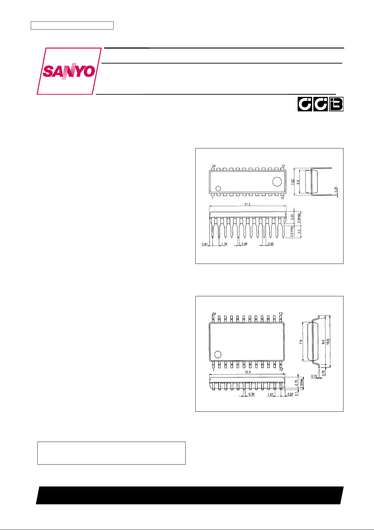
• Packages: DIP24S, MFP24
Package Dimensions
unit: mm
3067-DIP24S
unit: mm
3045B-MFP24
SANYO: DIP24S
[LC72720N]
SANYO: MFP24
[LC72720NM]
• CCB is a trademark of SANYO ELECTRIC CO., LTD.
• CCB is SANYO’s original bus format and all the bus
addresses are controlled by SANYO.
Single-Chip RDS
Signal-Processing System LSI
Pin Assignment
Block Diagram
No. 5877-2/14
LC72720N, 72720NM
T3 to T7
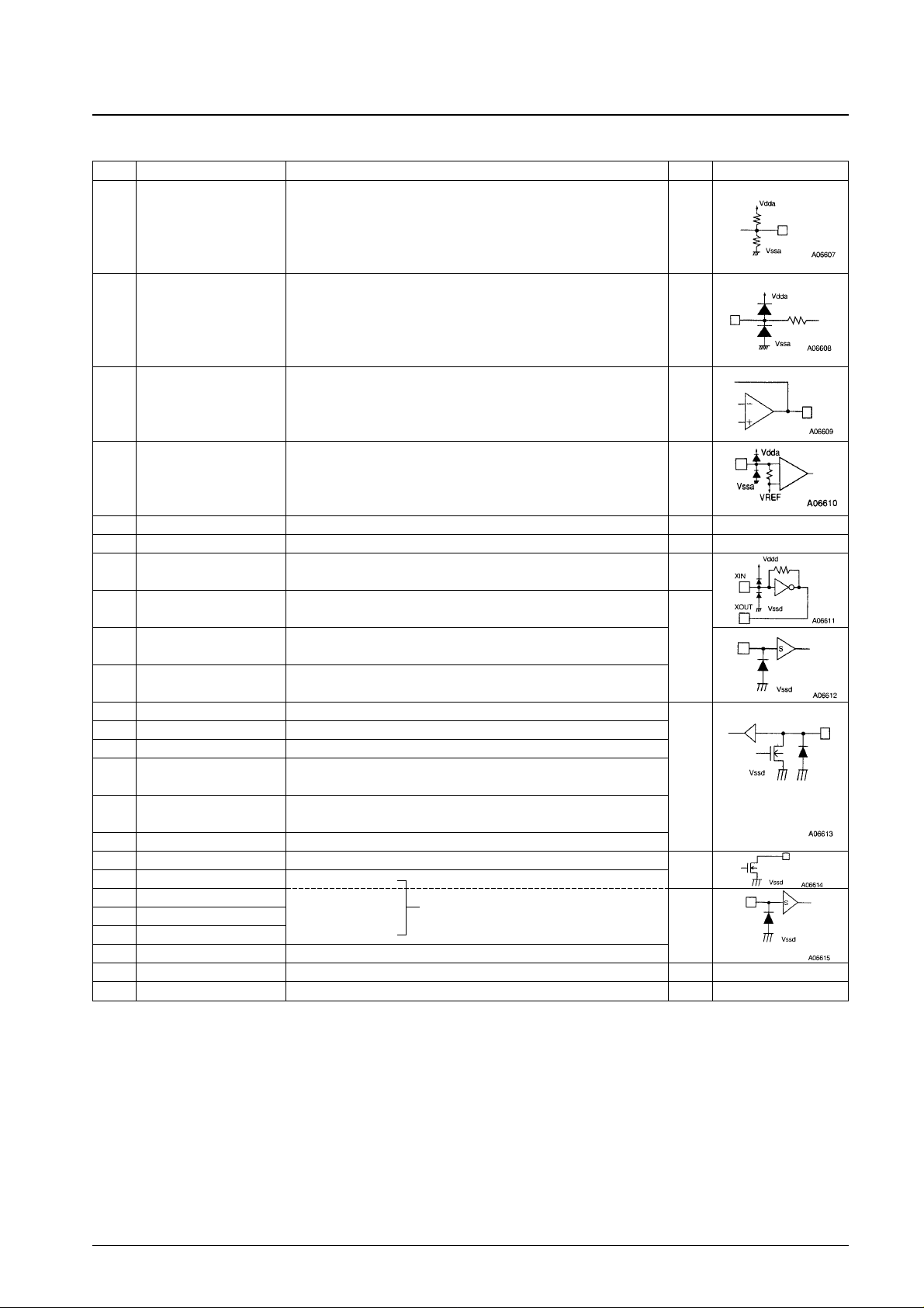
Pin Descriptions
No. 5877-3/14
LC72720N, 72720NM
Pin No. Pin name Function I/O Equivalent circuit
1 VREF Reference voltage output (Vdda/2) Output
2 MPXIN Baseband (multiplexed) signal input Input
5 FLOUT Subcarrier output (filter output) Output
6 CIN Subcarrier input (comparator input) Input
3 Vdda Analog system power supply (+5 V) — —
4 Vssa Analog system ground — —
12 XOUT Crystal oscillator output (4.332/8.664 MHz) Output
13 XIN Crystal oscillator input (external reference signal input)
7 T1 Test input (This pin must always be connected to ground.) Input
8 T2
Test input (standby control)
0: Normal operation, 1: Standby state (crystal oscillator stopped)
9 T3 (RDCL) Test I/O (RDS clock output)
10 T4 (RDDA) Test I/O (RDS data output)
11 T5 (RSFT) Test I/O (soft-decision control data output)
16 T6 (ERROR/57K/BE1)
Test I/O (error status output, regenerated carrier output, error block count
I/O*
output)
17 T7 (CORREC/ARI-ID/BE0)
Test I/O (Error correction status output, SK detection output, error block count
output)
18 SYNC Block synchronization detection output
19 RDS-ID RDS detection output
Output
20 DO Data output
21 CL Clock input
22 DI Data input
Input
23 CE Chip enable
24 SYR Synchronization and RAM address reset (active high)
14 Vddd Digital system power supply (+5 V) — —
15 Vssd Digital system ground — —
Note: * Normally function as an output pin. Used as an I/O pin in test mode, which is not available to user applications.
Serial data interface (CCB)
No. 5877-4/14
LC72720N, 72720NM
Parameter Symbol Conditions Ratings Unit
Maximum supply voltage V
DD
max Vddd, Vdda (Vdda ≤ Vddd + 0.3 V) –0.3 to +7.0 V
V
IN
1 max CL, DI, CE, SYR, T1, T2, T3, T4, T5, T6, T7, SYNC –0.3 to +7.0 V
Maximum input voltage V
IN
2 max XIN –0.3 to Vddd +0.3 V
V
IN
3 max MPXIN, CIN –0.3 to Vdda +0.3 V
V
O
1 max DO, SYNC, RDS-ID, T3, T4, T5, T6, T7 –0.3 to +7.0 V
Maximum output voltage V
O
2 max XOUT –0.3 to Vddd +0.3 V
V
O
3 max FLOUT –0.3 to Vdda +0.3 V
I
O
1 max DO, T3, T4, T5, T6, T7 6.0 mA
Maximum output current I
O
2 max XOUT, FLOUT 3.0 mA
I
O
3 max SYNC, RDS-ID 20.0 mA
Allowable power dissipation Pd max Ta ≤ 85°C
DIP24S: 350 mW
MFP24: 300 mW
Operating temperature Topr –40 to +85 °C
Storage temperature Tstg –55 to +125 °C
Specifications
Absolute Maximum Ratings at Ta = 25°C, Vssd = Vssa = 0 V
Parameter Symbol Conditions
Ratings
Unit
min typ max
Supply voltage
V
DD
1 Vddd, Vdda (Vddd = Vdda) 4.5 5.0 5.5 V
V
DD
2 Vddd: Serial data hold voltage 2.0 V
Input high-level voltage V
IH
CL, DI, CE, SYR, T1, T2 0.7 Vddd 6.5 V
Input low-level voltage V
IL
CL, DI, CE, SYR, T1, T2 0 0.3 Vddd V
Output voltage V
O
DO, SYNC, RDS-ID, T3, T4, T5, T6, T7 6.5 V
V
IN
1 MPXIN : f = 57 ±2 kHz 50 mVrms
Input amplitude V
IN
2 MPXIN : 100% modulation composite 100 mVrms
V
XIN
XIN 400 1500 mVrms
Guaranteed crystal oscillator frequencies Xtal
XIN, XOUT : CI ≤ 120 Ω (XS = 0) 4.332 MHz
XIN, XOUT : CI ≤ 70 Ω (XS = 1) 8.664 MHz
Crystal oscillator frequency deviation TXtal XIN, XOUT : f
O
= 4.322 MHz, 8.664 MHz ±100 ppm
Data setup time t
SU
DI, CL 0.75 µs
Data hold time t
HD
DI, CL 0.75 µs
Clock low-level time t
CL
CL 0.75 µs
Clock high-level time t
CH
CL 0.75 µs
CE wait time t
EL
CE, CL 0.75 µs
CE setup time t
ES
CE, CL 0.75 µs
CE hold time t
EH
CE, CL 0.75 µs
CE high-level time t
CE
CE 20 ms
Data latch change time t
LC
1.15 µs
t
DC
DO, CL: Differs depending on the value of the
0.46 µs
Data output time
pull-up resistor used.
t
DH
DO, CE: Differs depending on the value of the
0.46 µs
pull-up resistor used.
Allowable Operating Ranges at Ta = –40 to +85°C, Vssd = Vssa = 0 V
Parameter Symbol Conditions
Ratings
Unit
min typ max
Input resistance
Rmpxin MPXIN–Vssa : f = 57 kHz 23 kΩ
Rcin CIN–Vssa : f = 57 kHz 100 kΩ
Internal feedback resistance Rf XIN 1.0 MΩ
Center frequency fc FLOUT 56.5 57.0 57.5 kHz
–3 dB bandwidth BW – 3 dB FLOUT 2.5 3.0 3.5 kHz
Gain Gain MPXIN–FLOOUT : f = 57 kHz 28 31 34 dB
Att1 FLOUT : ∆f = ±7 kHz 30 dB
Stop band attenuation Att2 FLOUT : f < 45 kHz, f > 70 kHz 40 dB
Att3 FLOUT : f < 20 kHz 50 dB
Reference voltage output Vref VREF : Vdda = 5 V 2.5 V
Electrical Characteristics in the allowable operating ranges
Continued on next page.
Note: A capacitor of at least 1000 pF must be inserted between the power supply pins Vdd and Vss.
No. 5877-5/14
LC72720N, 72720NM
Parameter Symbol Conditions
Ratings
Unit
min typ max
Hysteresis V
HIS
CL, DI, CE, SYR, T1, T2 0.1 Vddd V
Output low-level voltage
V
OL
1 DO, T3, T4, T5, T6, T7 : I = 2 mA 0.4 V
V
OL
2 SYNC, RDS-ID : I = 8 mA 0.4 V
Input high-level current
I
IH
1 CL, DI, CE, SYR, T1, T2 : VI= 6.5 V 5.0 µA
I
IH
2 XIN : VI= Vddd 2.0 11 µA
Input low-level current
I
IL
1 CL, DI, CE, SYR, T1, T2 : VI= 0 V 5.0 µA
I
IL
2 XIN : VI= 0 V 2.0 11 µA
Output off leakage current I
OFF
DO, SYNC, RDS-ID, T3, T4, T5, T6, T7 :
5.0 µA
V
O
= 6.5 V
Current drain Idd Vddd + Vdda 12 mA
Continued from preceding page.
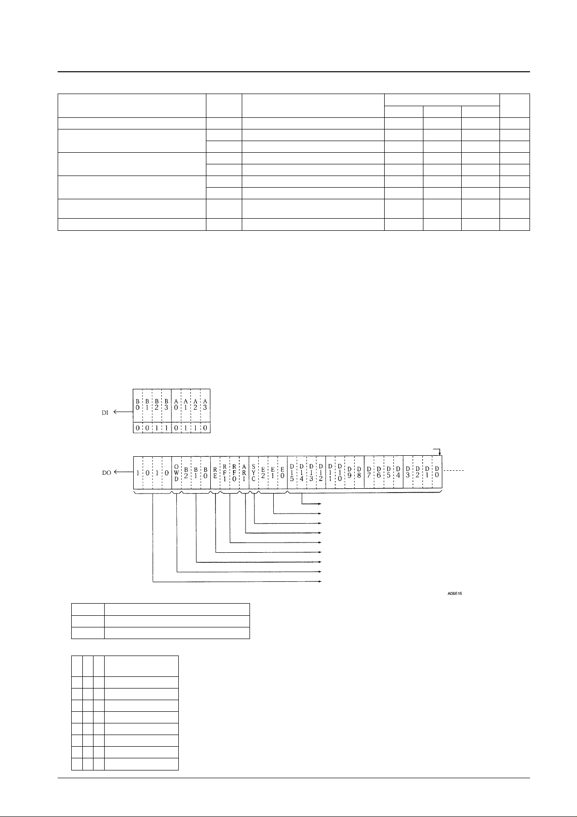
CCB Output Data Format
• Each block of output data consists of 32 bits (4 bytes), of which 2 bytes are RDS data and 2 bytes are flag data.
• Any number of 32-bit output data blocks can be output consecutively.
• When there is no data that can be read out in the internal memory, the system outputs blocks of all-zero data
consecutively.
• If data readout is interrupted, the next read operation starts with the 32-bit data block whose readout was interrupted.
However, if only the last bit remains to be read, it will not be possible to reread that whole block.
• The check bits (10 bits) are not output.
• To judge whether or not the data is valid, refer to the error information flags E0 to E2, but the offset word detection
flags (OWD) should never be reffered to.
• If the first four-bits are not “1010”, since the readout data is invalid, readout operation must be halted.
1. Offset word detection flag (1 bit): OWD
2. Offset word information flag (3 bits): B0 to B2
OWD Offset word detection
1 Detected
0 Not detected (protection function operating)
B B B
Offset word
2 1 0
0 0 0 A
0 0 1 B
0 1 0 C
0 1 1 C’
1 0 0 D
1 0 1 E
1 1 0 Unused
1 1 1 Unused
CCB address 6C
Output data/first bit Last bit
(8) RDS data
(7) Error information flags
(6) Synchronization established flag
(5) ARI (SK) detection flag
(4) RAM data remaining flag
(3) Consecutive RAM read out possible flag
(2) Offset word information flag
(1) Offset word detection flag
Fixed pattern (1010)
 Loading...