

Sanyo LC72713W Specifications
Ordering number : ENN6870A
92001TN (OT) No. 6870-1/29
Overview
The LC72713W is data demodulator ICs for receiving FM
multiplex broadcasts for mobile reception in the DARC
format. This IC includes an on-chip bandpass filter for
extracting the DARC signal from the FM baseband signal.
It also integrates a decoder circuit that performs the VICS
data processing on the same chip and can implement a
compact, multifunction VICS reception system. The
LC72713W is an improved version of the LC72710W that
features circuit improvements that allow a single tuner to
receive both the VICS data and the dGPS data supported
by the earlier device. Note that a contract with VICS
Center is required to evaluate this sample IC and to
produce end products that support VICS.
Functions
• Adjustment-free 76 kHz SCF bandpass filter
• Built-in VICS decoder
• MSK delay detection system based on a 1T delay.
• Error correction function based on a 2T delay (in the
MSK detection stage)
• Digital PLL based clock regeneration function
• Shift-register 1T and 2T delay circuits
• Block and frame synchronization detection circuits
• Functions for setting the number of allowable BIC errors
and the number of synchronization protection
operations.
• Error correction using (272, 190) codes
• Built-in layer 4 CRC code checking circuit
• On-chip frame memory and memory control circuit for
vertical correction
• 7.2 MHz crystal oscillator circuit
• Two power saving modes: STNBY and EC STOP
• Dedicated frame synchronization circuit for
simultaneous reception of dGPS and VICS data
• Applications can use either a parallel CPU interface
(DMA) or a CCB serial interface.
• Supply voltage: 4.5 to 5.5 V
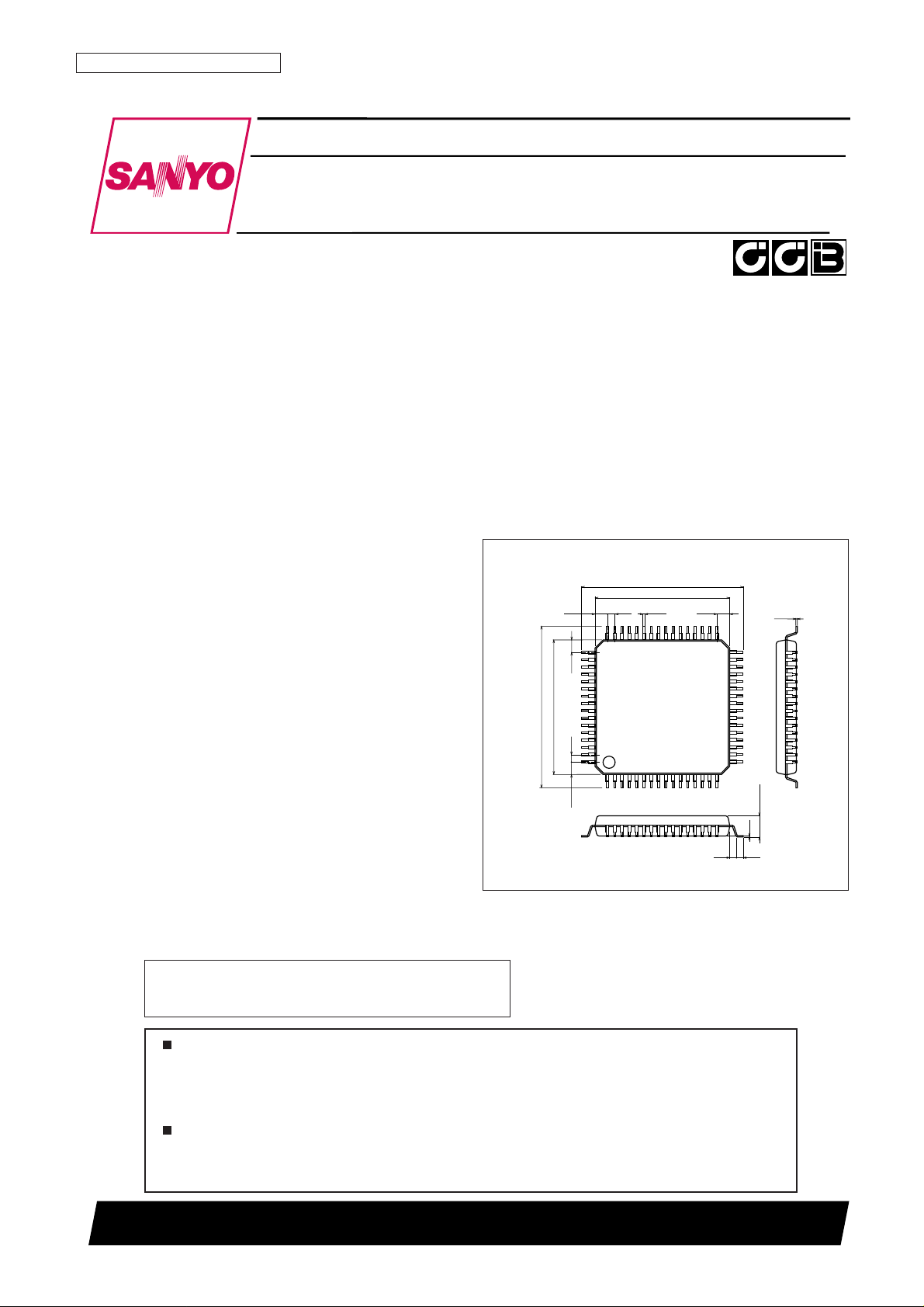
Package Dimensions
unit: mm
3190-SQFP64
10.0
12.0
1.25
0.51.25
1.25 0.5 1.250.18
12.0
116
17
32
33
48
49
64
10.0
0.5
1.7max
0.5
0.1
0.15
SANYO: SQFP64
[LC72713W]
LC72713W
SANYO Electric Co.,Ltd. Semiconductor Company
TOKYO OFFICE Tokyo Bldg., 1-10, 1 Chome, Ueno, Taito-ku, TOKYO, 110-8534 JAPAN
Mobile FM Multiplex Broadcast IC
with On-Chip VICS Decoder
CMOS IC
Any and all SANYO products described or contained herein do not have specifications that can handle
applications that require extremely high levels of reliability, such as life-support systems, aircraft’s
control systems, or other applications whose failure can be reasonably expected to result in serious
physical and/or material damage. Consult with your SANYO representative nearest you before using
any SANYO products described or contained herein in such applications.
SANYO assumes no responsibility for equipment failures that result from using products at values that
exceed, even momentarily, rated values (such as maximum ratings, operating condition ranges, or other
parameters) listed in products specifications of any and all SANYO products described or contained
herein.
• CCB is a trademark of SANYO ELECTRIC CO., LTD.
• CCB is SANYO’s original bus format and all the bus
addresses are controlled by SANYO.
No. 6870-2/29
LC72713W
Parameter Symbol Conditions Ratings Unit
Maximum supply voltage V
DD
–0.3 to +7.0 V
Input voltage
V
IN
(1) A0/CL, A1/CE, A2/DI, RST, STNBY –0.3 to +7.0 V
V
IN
(2) Pins other than VIN(1) –0.3 to VDD+ 0.3 V
Output voltage
V
OUT
(1) DO –0.3 to +7.0 V
V
OUT
(2) Pins other than V
OUT
(1) –0.3 to VDD+ 0.3 V
Output current
I
OUT
(1) INT, RDY, DREQ, and D0 to D15 0 to 4.0 mA
I
OUT
(2) Pins other than I
OUT
(1) 0 to 2.0 mA
Allowable output current (total) I
TTL
Total for all the output pins 20 mA
Allowable power dissipation Pdmax Ta ≤ 85°C 200 mW
Operating temperature Topr –40 to +85 °C
Storage temperature Tstg –55 to +125 °C
Specifications
Absolute Maximum Ratings at Ta = 25°C, VSS= 0 V
Parameter Symbol Conditions
Ratings
Unit
min typ max
Supply voltage V
DD
4.5 5.5 V
High-level input voltage
V
IH
1 A0/CL, A1/CE, A2/DI, RST, STNBY 0.7 V
DD
5.5 V
V
IH
2 DACK, WR, RD, CS, SP, BUSWD, A3, IOCNT1, IOCNT2 0.7 V
DD
V
DD
V
Low-level input voltage
V
IL
1 Pins for which VIH1 applies V
SS
0.3 V
DD
V
V
IL
2 Pins for which VIH2 applies V
SS
0.3 V
DD
V
Oscillator frequency FOSC This IC operates with a frequency precision of ±250 ppm 7.2 MHz
X
IN
input sensitivity VXI
With a sine wave input to X
IN
, capacitor coupling,
400 1500 mVrms
V
DD
= +4.5 to +5.5 V
Input amplitude VMPX
With a 100% modulated composite signal input to
150 500 mVrms
MP
XIN
, VDD= +4.5 to +5.5 V
Clock low-level period t
CL
A0/CL 0.7 µs
Clock high-level period t
CH
A0/CL 0.7 µs
Data setup time t
SU
A0/CL, A2/DI 0.7 µs
Data hold time t
HD
A0/CL, A2/DI 0.7 µs
CE wait time t
EL
A0/CL, A1/CE 0.7 µs
CE setup time t
ES
A0/CL, A1/CE 0.7 µs
CE hold time t
EH
A0/CL, A1/CE 0.7 µs
Data latch change time t
LC
A1/CE 0.7 µs
Data output time t
DDO
DO, A0/CL 277 555 ns
CRC4 change time t
CRC
CRC4, A0/CL 0.7 µs
Allowable Operating Ranges at Ta = –40 to +85°C, VSS= 0 V
Serial I/O
No. 6870-3/29
LC72713W
Allowable Operating Ranges: Parallel Interface at Ta = –40 to +85°C, VSS= 0 V
Notes: Application designs must take the RDY signal output delay into consideration if the RDY signal is used as the CPU bus wait signal.
When the RDY signal is used, the “RD low-level width” and the “Corrected output RD width” values express the basic timing (excluding the wait
time) settings for the CPU bus.
If the RDY signal is not used, (that is, if no wait states are inserted) the value of the RD low-level width will be 250 ns (minimum).
Parameter Symbol Conditions
Ratings
Unit
min typ max
Address to RD setup t
SARD
A0/CL, A1/CE, A2/DI, A3, RD 20 ns
RD to address hold t
HARD
A0/CL, A1/CE, A2/DI, A3, RD, t
WRDL
=>250 ns –20 ns
RD low-level width t
WRDL
1 RD 250 ns
RD low-level width (when RDY is used) t
WRDL
2 RD 100 250 ns
RD cycle wait t
CYRD
A0/CL, A1/CE, A2/DI, A3, RD 150 ns
RDY width (Register read) t
WRDY
RDY 60 210 ns
RD data hold t
RDH
RD, DATn 0 ns
Address to WR setup t
SAWR
A0/CL, A1/CE, A2/DI, A3, WR 20 ns
WR to address hold t
HAWR
A0/CL, A1/CE, A2/DI, A3, WR 20 ns
WR cycle wait t
CYWR
A0/CL, A1/CE, A2/DI, A3, WR 150 ns
WR low-level width t
WWRL
WR 200 ns
WR data hold t
WDH
WR, DATn 0 ns
RDY output delay t
DRDY
RD, RDY 0 30 ns
Corrected output RD width t
WDRD
1
RD (BUSWD = L 8 bits) 300 ns
RD (BUSWD = H 16 bits) 540 ns
Corrected output RD width
t
WDRD
2
RD (BUSWD = L 8 bits) 100 300 ns
(when RDY is used) RD (BUSWD = H 16 bits) 300 540 ns
RDY width (corrected output read) t
WDRDY
RDY (BUSWD = L 8 bits) 60 210 ns
RDY ((BUSWD = H 16 bits) 300 490 ns
DACK to DREQ delay t
DREQ
DREQ, DACK 260 ns
DMA cycle wait t
CYDM
RD, DREQ 420 ns
RD low-level width (DMA) t
WRDM
RD 300 ns
Parallel I/O
Electrical Characteristics at VDD= +4.5 to +5.5 V, within the allowable operating ranges
Parameter Symbol Conditions
Ratings
Unit
min typ max
V
OH
1
Io = 2 mA, BCK, FCK, BLOCK, FLOCK,
VDD– 0.4 V
High-level output voltage
CRC4, CLK16DATA
V
OH
2 Io = 4 mA, INT, RDY, DREQ, D0 to D15 VDD– 0.4 V
V
OL
1 Io = 2 mA, Pins for which VOH1 applies 0.4 V
Low-level output voltage V
OL
2 Io = 4 mA, Pins for which VOH2 applies 0.4 V
V
OL
3 Io = 2 mA, DO, INT 0.4 V
I
IH
1
V
IN
= 5.5 V, A0/CL, A1/CE, A2/DI, RST,
1.0 µA
High-level input current
STNBY
I
IH
2 VIN= V
DDD
, All input pins other than IIH1 1.0 µA
Low-level input current I
IL
VIN= V
SSD
, All input pins –1.0 µA
Input resistance Rmpx MP
XIN
– Vssa f = 100 kHz 50 kΩ
Reference supply voltage output Vref Vref, Vdda = 5 V 2.5 V
Bandpass filter center frequency Fc FLOUT 76.0 kHz
–3 dB bandwidth Fbw FLOUT 19.0 kHz
Group delay Dgd FLOUT –7.5 +7.5 µs
Gain Gain FLOUT – MPXIN f = 76 kHz 20 dB
ATT1 FLOUT f = 50 kHz 25 dB
Stop band attenuation
ATT2 FLOUT f = 100 kHz 15 dB
ATT3 FLOUT f = 30 kHz 50 dB
ATT4 FLOUT f = 150 kHz 50 dB
Output off leakage current IOFF V0 = V
DDD
, DO 5.0 µA
Hysteresis voltage VHIS
A0/CL, A1/CE, A2/DI, A3, CS, RD, WR,
0.1 V
DDD
V
DACK, IOCNT1, IOCNT2, RST, STNBY
Internal feedback resistor Rf XIN, XOUT 1.0 MΩ
Current drain I
DD
18 25 mA
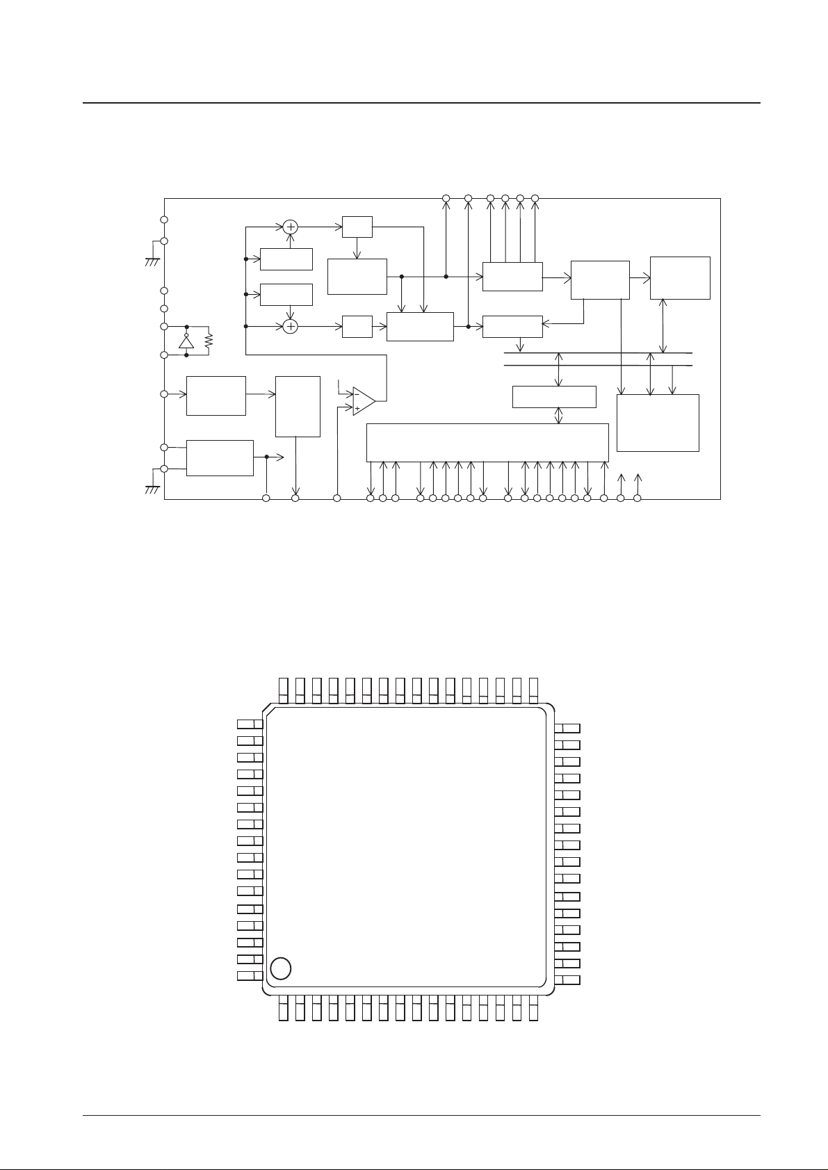
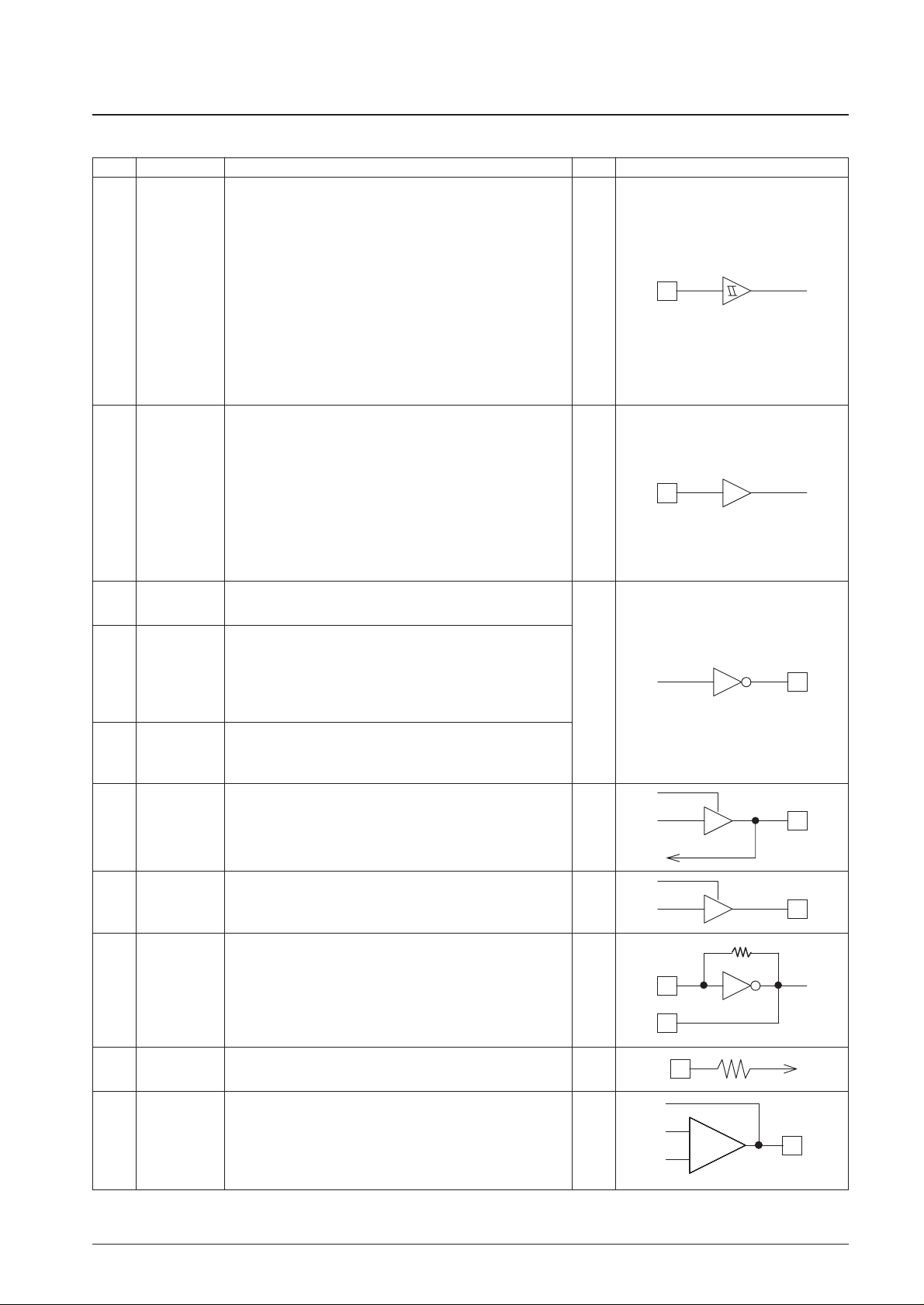
Block Diagram
No. 6870-4/29
LC72713W
VICS processing
PN decoding
Memory array
LPF
MPXIN
7.2MHz
Vref
XIN
Vssa
Vdda
XOUT
RST
CLK16
DATA
BCK
FCK
FLOCK
BLOCK
Data
Address
STNBY
Vssd
Vddd
LPF
Error correction:
layer 2 CRC
76kHz
BPF
(SCF)
Anti-aliasing
filter
Timing
control
Vref
Synchronization
regeneration
MSK correction
circuit
Clock
regeneration
2T delay
1T delay
IOCNT1
DACK
DREQ
IOCNT2
CRC4
FLOUT
CIN
VREF
CS
RD
WR
RDY
INT
BUSWD
TIN
SP
A3
DO
A2/DI
A1/CE
A0/CL
D0 to D15
Output control (CPU interface) and
layer 4 CRC detection circuit
Pin Assignment
IOCNT1
WR
RD
A0/CL
A1/CE
A2/DI
A3
CS
STNBY
BUSWDSPRST
32
D15
49
D14
D13
TIN
LC72713W
Vssa
D12
Vref
MPXIN
D11
D10
Vdda
D9
FLOUT
D8
NC
NC
CIN
D7
D6
TPC1
(Top view)
64
1
16
D5
TPC2
BCK
CRC4
FCK
BLOCK
FLOCK
DATA
CLK16
IOCNT2
Vddd
XOUT
INT
Vddd
Vssd
DO
NC
TEST
TOSEL1
TOSEL2
Vssd
XIN
Vddd
RDY
Vssd
DACK
DREQ
D4
D3
D2
D1
D0
No. 6870-5/29
LC72713W
Pin Functions
Pin No. Pin Function I/O Pin circuit
Data bus I/O control 1 (SP = low)*
1
Data bus I/O control 2 (SP = low)*
1
DMA acknowledge (SP = low)*
1
Write control signal (SP = low)*
1
Read control signal (SP = low)*
1
Address input 0 (SP = low) CCB CL input (SP = low)
1 (SP = low) CCB CE input (SP = low)
2 (SP = low) CCB DI input (SP = low)
3 (SP = low)*
1
Chip select input (SP = L)*
1
System reset input (negative logic)
Standby mode (positive logic)
3
4
13
38
39
40
41
42
43
44
46
45
IOCNT1
IOCNT2
DACK
WR
RD
A0/CL
A1/CE
A2/DI
A3
CS
RST
STNBY
SP = low: parallel, SP = high: serial
BUSWD = low: 8 bits, BUSWD = high: 16 bits
The test pin must be connected to the digital system ground (V
SS
).
Must be connected to the digital system power supply (V
DD
) or ground
(VSS) in normal operation.
As above
As above
As above
As above
47
48
60
58
59
61
62
49
SP
BUSWD
TEST
TPC1
TPC2
TOSEL1
TOSEL2
TIN
Clock regeneration monitor
Demodulated data monitor
5
6
CLK16
DATA
Frame start signal output
Block start signal output
Outputs a high level during frame synchronization
Outputs a high level during block synchronization
Level 4 CRC detection result output
9
10
7
8
11
FCK
BCK
FLOCK
BLOCK
CRC4
External CPU interrupt request output
DMA request signal
Read ready signal
Input
Input
Output
I/O
33
12
16
INT
DREQ
RDY
Data bus
The bus width can be set to be either 8 bits or 16 bits by the BUSWD
pin (pin 48).
For data input, only the lower 8 bits (D0 to D7) are valid. *
3
17 to 24 D0 to D7
Output
Data bus (in 16-bit mode)
These pins are held in the output off state when BUSWD is low.
25 to 32 D8 to D15
I/O
Connections for the system clock crystal oscillator circuit.
The XIN pin can also be used as an external clock signal input.
64
1
XIN
XOUT
InputBaseband (multiplex) signal input53 MPXIN
–
+
OutputSubcarrier output (76 kHz bandpass filter output)55 FLOUT
Continued on next page.
No. 6870-6/29
LC72713W
Continued from preceding page.
Pin No. Pin Function I/O Pin circuit
Subcarrier input (comparator input)56 CIN
Vref
–
+
Input
Reference voltage output (Vdda/2)52 VREF
Vssa
Vdda
Output
CCB serial interface data output36 DO
Output
—
—
—
—
This pin must be left open
37
50
57
NC
Analog system power supply
Analog system ground
Digital system power supply (+4.5 V to +5.5 V)
Digital system ground
54
51
2, 15, 34
14, 35, 63
V
DDA
V
SSA
V
DDD
V
SSD
Notes: 1. This pin must be connected to V
DDD
or V
SSD
if the IC is used in serial interface mode (when SP is high).
2. A capacitor of at least 2000 pF must be inserted between V
DDD
and V
SSD
.
3. When used in the SP = high mode (as set by the serial interface), the D0 to D7 data bus lines must be connected to either V
DDD
or V
SSD
.
Control Registers
This IC includes both registers that can be read and registers that can be written. These registers can be accessed using
either the serial interface (CCB) or the parallel interface. The SP pin switches between these interfaces.
The initial values of the write registers are the data loaded into internal registers when a reset signal (RST) is received.
These values are recommended values that do not need to be changed during normal operation.
If the parallel interface is used, applications must hold the address fixed at 00H when reading out data to which error
correction has been applied. If the CCB interface is used, the application needs only to specify the CCB address (#FB).
The address 00H is an invalid address for writing.
The addresses other than those specified below are control addresses particular to the IC. Applications must not specify
those addresses.
Address Register Function R/W Address Register Function R/W
1 BIC Number of allowable BIC errors W 1 STAT Status register R
2 SYNCB Block synchronization: error protection count W 2 BLNO Block number register R
3 SYNCF Frame synchronization: error protection count W
4 CTL1 Control register 1 W
5 CTL2 Control register 2 W
6 CRC4 Layer 4 CRC register W
The synchronization circuit in this IC operates by recognizing a 16-bit BIC code. The number of allowable errors is the
number of incorrect bits allowed in those 16 bits. This data sets up separate values for forward protection mode (when
synchronized) and for back protection mode (when not synchronized).
The default value is to allow 2 incorrect bits in both forward and back modes. If the block synchronization discrimination
output (BLOCK) is used for discriminating whether or not FM multiplex data is present, we recommend setting the back
protection mode BIC allowable error count to 1 or 0.
No. 6870-7/29
LC72713W
Number of Allowable BIC Errors
Address Register R/W Initial value BIT7 BIT6 BIT5 BIT4 BIT3 BIT2 BIT1 BIT0
01H BIC W 22H Back protection (LSB) Forward protection (LSB)
The synchronization protection count can be set separately for both forward and back protection. The count conditions
for the protection counts are as follows.
• Back protection mode (not synchronized: BLOCK = low)
If the timing of the IC internal synchronization free-running counter matches the timing of the received BIC, the
protection count is incremented by 1. Contrarily, if the timings of the IC internal counter and the received BIC do not
match, the protection counter is cleared to 0. The timing of the count is the timing of the IC internal counter.
• Forward protection mode (synchronized: BLOCK = high)
In reverse to the back protection mode, if the timing of the IC internal free-running counter does not match the
detection timing of the received BIC, the protection counter is incremented, and if the timings match, the protection
counter is cleared to 0.
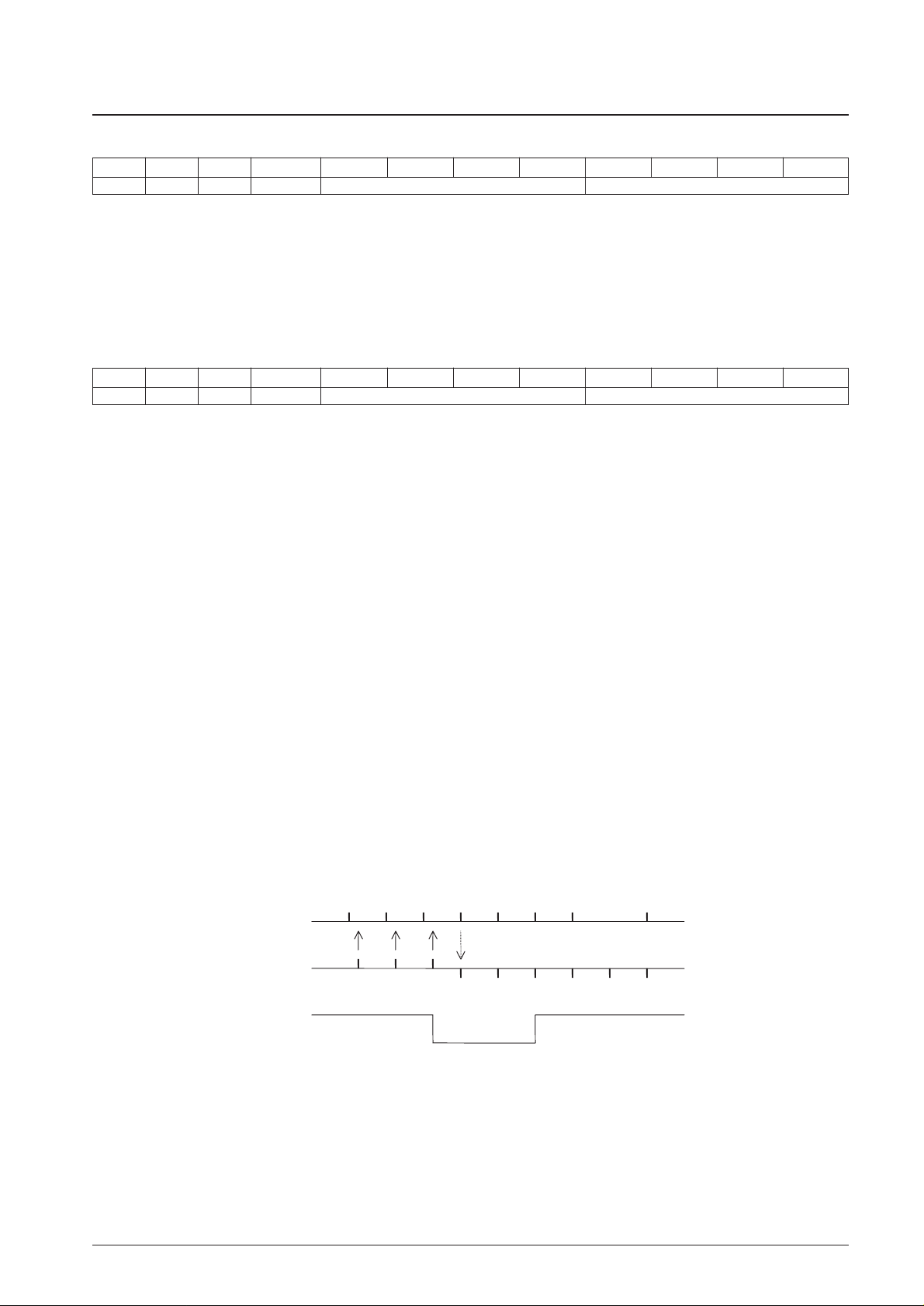
Figure 1 shows the states of the protection counter for the cases where the forward and back protection counts are both 3.
This IC defines the value of the protection counter to be 1 at the point that a match or a discrepancy occures between the
IC internal timing and the timing of the received BIC. For example, when the value of the back protection count is 2, the
IC internal timing and the timing of the received BIC will have matched two times consecutively.
If the protection data is set to new values, for example if the protection counts are set to 3 as assumed in figure 1,
applications must send values which are 1 less than the intended value; in this case 22H. Similarly, if the value is set to
00H, the protection counts will, by definition, be set to 1 for both the forward and back directions. However, note that the
resulting operation will be equivalent to there being no protection circuit. The default values are 8 for the forward
protection count and 2 for the back protection count.
If the block synchronization output (BLOCK) is used for discriminating whether or not FM multiplex data is present, we
recommend setting the block synchronization back protection count to a value that is more strict than the default value.
(That is, we recommend replacing the default value of 2 with a value of 3 or higher.)
Block Synchronization: Error Protection Count
Address Register R/W Initial value BIT7 BIT6 BIT5 BIT4 BIT3 BIT2 BIT1 BIT0
02H SYNCB W 17H Back protection (LSB) Forward protection (LSB)
Figure 1 Block Synchronization Protection Operation (Forward → Back → Forward)
Received data
Synchronization
counter BIC position
Block
BIC
321
Reset
1
32
* Assumes that the forward and
back protection counts are 3.
010
No. 6870-8/29
LC72713W
This IC detects the BIC characteristic inflection points which occur at four places in a single frame, and increments or
decrements a protection counter depending on whether or not they match the IC internal frame synchronization timing
counter.
As is the case with the block synchronization error protection value, applications must set these to values one less than
the desired protection count. The default values are 8 for the frame synchronization forward protection count and 2 for
the back protection count.
Frame Synchronization: Error Protection Count
Address Register R/W Initial value BIT7 BIT6 BIT5 BIT4 BIT3 BIT2 BIT1 BIT0
03H SYNCF W 17H Back protection (LSB) Forward protection (LSB)
*: BIT0 and BIT1 are unused.
• VEC_HALT
0: Vertical correction and the second horizontal correction processing are performed. (default)
1: Vertical correction and the second horizontal correction processing are not performed.
All IC operations related to vertical correction and the second horizontal correction are stopped by setting this flag.
Note that in data output, only data to which the first horizontal correction has been applied will be output.
• EC_STOP
0: All functions operate. (default)
1: Only the MSK detection circuit and the synchronization regeneration circuit operate.
This flag stops all operations relating to error correction (including RAM access), data output, and other operations.
While all IC operations are stopped in standby mode, MSK demodulation, the synchronization circuit, the serial data
input circuit, and the layer 4 CRC circuit continue to operate in this mode.
• SYNC_RST
0: (default)
1: Resets just the synchronization regeneration circuit.
Clears the synchronization status and the synchronization protection status in the synchronization circuit block, and
sets the circuit to the unsynchronized state. This allows the circuit to quickly pull in to frame synchronization when
the frame synchronization is incorrect for the new reception data following tuning, when the radio has been tuned to
a new station. While this flag is used for synchronization related sections of the system, it does not initialize the
registers that set the number of allowable BIC errors, the block synchronization forward and back protection counts,
and the frame synchronization forward and back protection counts. Also note that during a synchronization block
reset, the INT signal is not output and the DO pin outputs a high level (high-impedance).
This flag is not automatically reset to 0. Applications must send a 0 value after setting this flag.
Control Register 1
Address Register R/W Initial value BIT7 BIT6 BIT5 BIT4 BIT3 BIT2 BIT1 BIT0
04H CTL1 W 00H CRC4_RST DO_MOVE INT_MOVE SYNC_RST EC_STOP VEC_HALT * *
• INT_MOVE
0: Data is only output when error correction has completed, layer 2 CRC has completed, and the data was received with
the circuit synchronized. (default)
1: All data is output. (Operation is identical to that of the LC72700E.)
In the default state, this IC only outputs data that has been fully error corrected and that was received in both block
and frame synchronization. (This also includes the layer 2 CRC check.)
To acquire all data as provided by the LC72700, applications must set both this flag and the VEC_OUT (BIT2) flag
in control register 2 as described below.
• DO_MOVE (Valid only when SP is high.)
0: The high state (high impedance) is held at all times other than when data is being output. (default)
1: Operate identically to the LC72700 when changes are linked to the INT signal, i.e. when both INT_MOVE and
VEC_OUT are set to 1.
• CRC4_RST
0: (default)
1:Reset the layer 4 CRC detection circuit.
This flag is not automatically reset to 0. Applications must send a 0 value after setting this flag.
No. 6870-9/29
LC72713W
• DMA (Valid only when SP is low.)
0: Do not use DMA transfer for readout of post-error correction data. (default)
1: Use DMA transfer for readout of post-error correction data.
• DMA_RD (Valid only when SP is low.)
0: Use the RD signal as the DMA transfer read control signal. (default)
1: Use the DACK signal as the DMA transfer read control signal.
• VEC_OUT
0: Do not perform post-horizontal correction output when vertical correction processing is not performed. (default)
1: Output all data, even when vertical correction processing is not performed. (Operation identical to that of the
LC72700)
When this flag is set and a frame of data with absolutely no errors is received, data that is completely identical to the
corresponding post-horizontal correction data is output with the timing of the output of post-vertical correction data,
even if vertical correction is not performed.
This flag must be set to create interface specifications identical to those of the LC72700.
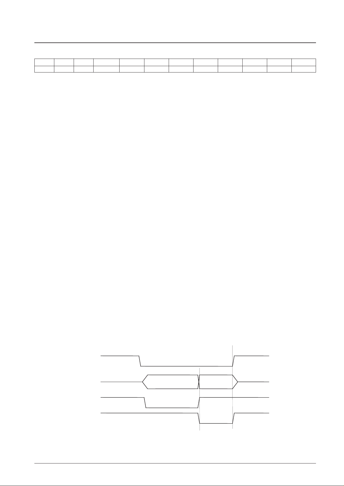
• RDY (Valid only when SP is low.)
0: The RDY output is issued with timing 1. (default)
1: The RDY output is issued with timing 2.
• DREQ (Valid only when SP is low.)
0: Negative logic is used for the polarity of the DREQ signal. (default)
1: Positive logic is used for the polarity of the DREQ signal.
• DACK (Valid only when SP is low.)
0: Negative logic is used for the polarity of the DACK signal. (default)
1: Positive logic is used for the polarity of the DACK signal.
• BLK_RST
0: (default)
1: Resets the block synchronization circuit only.
Sets the block synchronization status to unsynchronized and clears the block synchronization protection counter.
However, note that this has no effect on the frame synchronization functions. Also note that during a
synchronization block reset, the INT signal is not output and the DO pin outputs a high level (high-impedance).
This flag is not automatically reset to 0. Applications must send a 0 value after setting this flag.
• SUBBLK
0: Normal status. (default)
1: Set to 1 when a substation (for example a dGPS station during VICS reception) is temporarily received.
The SUBBLK and BLK_RST flags are mainly used when receiving and processing VICS data and dGPS data at the
same time. (See page 28.)
Control Register 2
Address Register R/W Initial value BIT7 BIT6 BIT5 BIT4 BIT3 BIT2 BIT1 BIT0
05H CTL2 W 00H SUBBLK BLK_RST DACK DREQ RDY VEC_OUT DMA_RD DMA
RDY Signal Output Timing
RD
DATn
RDY
Timing1
RDY
Timing2
Valid
output
 Loading...