

SANYO LC72709W, LC72709E Datasheet

Overview
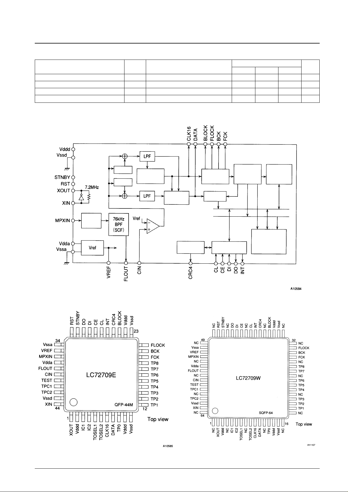
The LC72709E is a data demodulation IC for receiving
FM multiplex broadcasts for mobile receivers in the
DARC format. This IC includes a built-in bandpass filter
that extracts the DARC signal from the FM baseband
signal. Since this IC supports all of the FM multiplex
broadcast frame structures (methods A, A', B, and C) from
the ITU-R recommendations, it is optimal for use in radios
for worldwide use that support FM multiplex reception.
Functions
• SCF-based adjustment-free 76-kHz bandpass filter
• Support for the FM multiplex broadcast frame structures
(methods A, B, and C) using serial data control.
• MSK delay detection circuit based on a 1T delay
• Error correction function based on a 2T delay (in the
MSK detector stage)
• Digital PLL based clock regeneration circuit
• Shift-register type 1T and 2T delay circuits
• Block and frame synchronization detection circuit
• Function for setting the number of allowable BIC errors,
the number of synchronization protection.
• Error correction using (272, 190) codes
• Layer 4 CRC code checking circuit
• On-chip frame memory and memory control circuit for
vertical correction
• 7.2-MHz crystal oscillator circuit
• Two power saving functions (Standby and EC stop)
Package Dimensions
unit: mm
3148-QIP44MA
unit: mm
3190-SQFP64
CMOS IC
71598RM (OT) No. 5876-1/16
SANYO: QIP44MA
[LC72709E]
SANYO: SQFP64
[LC72709W]
SANYO Electric Co.,Ltd. Semiconductor Bussiness Headquarters
TOKYO OFFICE Tokyo Bldg., 1-10, 1 Chome, Ueno, Taito-ku, TOKYO, 110-8534 JAPAN
FM Multiplex Reception IC for Mobile Systems
LC72709E, 72709W
Ordering number : EN5876
• CCB is a trademark of SANYO ELECTRIC CO., LTD.
• CCB is SANYO’s original bus format and all the bus
addresses are controlled by SANYO.

No. 5876-2/16
LC72709E, 72709W
Parameter Symbol Conditions Ratings Unit
Maximum supply voltage V
DD
max –0.3 to +7.0 V
Input voltage
V
IN
1 CE, CL, DI, RST, STNBY –0.3 to +7.0 V
V
IN
2 Pins other than VIN1 –0.3 to VDD+0.3 V
Output voltage
V
OUT
1 DO –0.3 to +7.0 V
V
OUT
2 Pins other than V
OUT
1 –0.3 to VDD+0.3 V
Output current I
OUT
BLOCK, FLOCK, BCK, FCK, DO 0 to 4.0 mA
Allowable power dissipation Pd max
LC72709E 250 mW
LC72709W 200 mW
Operating temperature Topr Ta ≤ 85°C –40 to +85 °C
Storage temperature Tstg –55 to +125 °C
Specifications
Absolute Maximum Ratings at Ta = 25°C, VSS= 0 V
Parameter Symbol Conditions
Ratings
Unit
min typ max
Supply voltage V
DD
4.5 5.5 V
Input high-level voltage V
IH
CL, CE, DI, RST, STNBY 0.7 V
DD
5.5 V
Input low-level voltage V
IL
CL, CE, DI, RST, STNBY V
SS
0.3 V
DD
V
Oscillator frequency F
OSC
This IC operates at frequencies within a
7.2 MHz
±250 ppm precision
Input sensitivity V
XI
With a capacitance-coupled sine wave input
400 1500 mVrms
to X
IN
Input amplitude V
MPX
MPXIN, 100% modulation composite 150 500 mVrms
[Serial I/O*]
Clock low-level time t
CL
CL 0.7 µs
Clock high-level time t
CH
CL 0.7 µs
Data setup time t
SU
CL, DI 0.7 µs
Data hold time t
HD
CL, DI 0.7 µs
CE wait time t
EL
CL, CE 0.7 µs
CE setup time t
ES
CL, CE 0.7 µs
CE hold time t
EH
CL, CE 0.7 µs
Data latch change time t
LC
CE 0.7 µs
Data output time t
DD0
DO, CL 277 555 ns
Layer 4 CRC change time t
CRC
CRC4, CL 0.7 µs
Allowable Operating Ranges at Ta = –40 to +80°C, VSS= 0 V
Note *: See the serial data timing chart.
Parameter Symbol Conditions
Ratings
Unit
min typ max
Output high-level voltage V
OH
1
I
O
= 2 mA, BCK, FCK, BLOCK, FLOCK,
V
DD
– 0.4 V
CRC4, INT, CLK16, DATA, IC1, IC2
Output low-level voltage
V
OL
1 IO= 2 mA, applies to the same pins as VOH1 0.4 V
V
OL
2 IO= 2 mA, DO 0.4 V
Input high-level current
I
IH
1 VIN= 5.5 V, CE, CL, DI, RST, STNBY 1.0 µA
I
IH
2 VIN= VDDD, input pins other than IIH1 1.0 µA
Input low-level current I
IL
VIN= VSSD, CL, CE, DI, RST, STNBY,
–1.0 µA
TP0 to TP8, TPC1 to 2, TOSEL1 to 2, TEST
Input resistance R
MPX
MPXIN-Vssa, f = 0 to 100 kHz 50 kΩ
Reference supply voltage output V
REFVREF
, Vdda = 5 V 2.5 V
Bandpass filter center frequency F
C
FLOOUT 76.0 kHz
–3 dB bandwidth F
BW
FLOUT 19.0 kHz
In-band delay time difference D
GD
FLOUT ±5 µs
Gain Gain MPXIN-FLOUT, f = 76 kHz 20 dB
ATT1 FLOUT, f = 50 kHz 25 dB
Stop band attenuation
ATT2 FLOUT, f = 100 kHz 15 dB
ATT3 FLOUT, f = 30 kHz 50 dB
ATT4 FLOUT, f = 150 kHz 50 dB
Electrical Characteristics at VDD= 4.5 to 5.5 V, in the allowable operating ranges
Continued on next page.
No. 5876-3/16
LC72709E, 72709W
Block Diagram
Pin Assignments
1T delay
Synchronization
regeneration
PN
decoding
Output control
(CPU interface)
Antialiasing
filter
Timing control
Memory array
Error
correction
Layer 2 CRC
Data
Address
Layer 4 CRC
2T delay
Clock
regeneration
MSK
correction
Parameter Symbol Conditions
Ratings
Unit
min typ max
Output off leakage current I
OFFVO
= VDDD, DO 5 µA
Hysteresis voltage V
HIS
CL, CE, DI, RST, STNBY 0.1 V
DD
V
Internal feedback resistor R
f
XIN, X
OUT
1.0 MΩ
Current drain I
DD
18 25 mA
Continued from preceding page.
No. 5876-4/16
LC72709E, 72709W
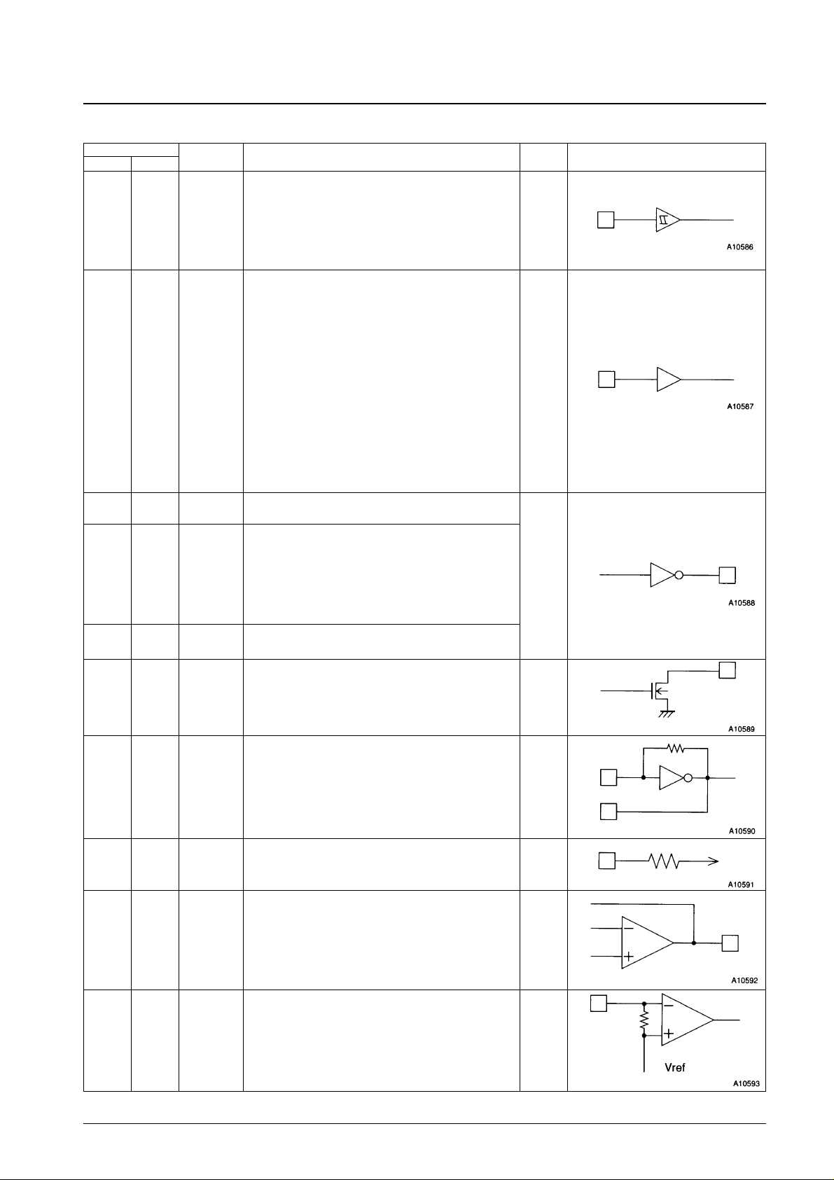
Pin Descriptions
Pin No.
Pin Name Function I/O Circuit type
LC72709E LC72709W
CL
CE
DI
RST
STNBY
TEST
28
29
30
33
32
40
CCB serial interface Clock input
Data control input
Data input
System reset input (active low)
Standby mode (active high)
Test (Must be connected to ground during normal operation.)
Input
Input
TP0
TP1
TP2
TP3
TP4
TP5
TP6
TP7
TP8
TPC1
TPC2
TOSEL1
TOSEL2
9
12
13
14
15
16
17
18
19
41
42
5
6
Must be connected to either V
DD
or VSS.
Output
Output
CLK16
DATA
FCK
BCK
FLOCK
BLOCK
CRC4
INT
7
8
20
21
22
25
26
27
Clock regeneration monitor
Demodulated data monitor
Frame start signal output
Block start signal output
Outputs a high level during frame synchronization.
Outputs a high level during block synchronization.
Layer 4 CRCC check result output
External CPU interrupt signal
IC1
IC2
3
4
Internal connections. These pins must be left open.
DO31 Data output used by the CCB serial interface
Input
Output
XIN
XOUT
44
1
System clock generation crystal oscillator element
connections
InputMPXIN36 Baseband (multiplex) signal input
OutputFLOUT38 Subcarrier output (76-kHz filter output)
InputCIN39 Subcarrier input (comparator input)
40
42
43
47
46
58
13
18
19
20
22
23
24
26
27
59
61
7
9
10
11
29
30
31
36
38
39
5
6
44
63
2
52
55
57
Continued on next page.
No. 5876-5/16
LC72709E, 72709W
Continued from preceding page.
Pin No.
Pin Name Function I/O Circuit type
LC72709E LC72709W
Output
VDDA
V
SS
A
V
DD
D
V
SS
D
54
50
3, 14, 35,
15, 34, 62
37
34
2, 10, 24
11,23, 43
Analog system power supply
Analog system ground
Digital system power supply (4.5 to 5.5 V)
Digital system ground
—
—
—
—
NC
1, 4, 8,
12, 16,
17, 21,
25, 28,
32, 33,
37, 41,
45, 48,
49, 53,
56, 60,
64
– Not connection
Note: A capacitor of at least 2000 pF must be inserted between VDDD and VSSD when using this IC.
V
REF
35 Reference voltage output (Vdda/2)51
Data I/O Techniques
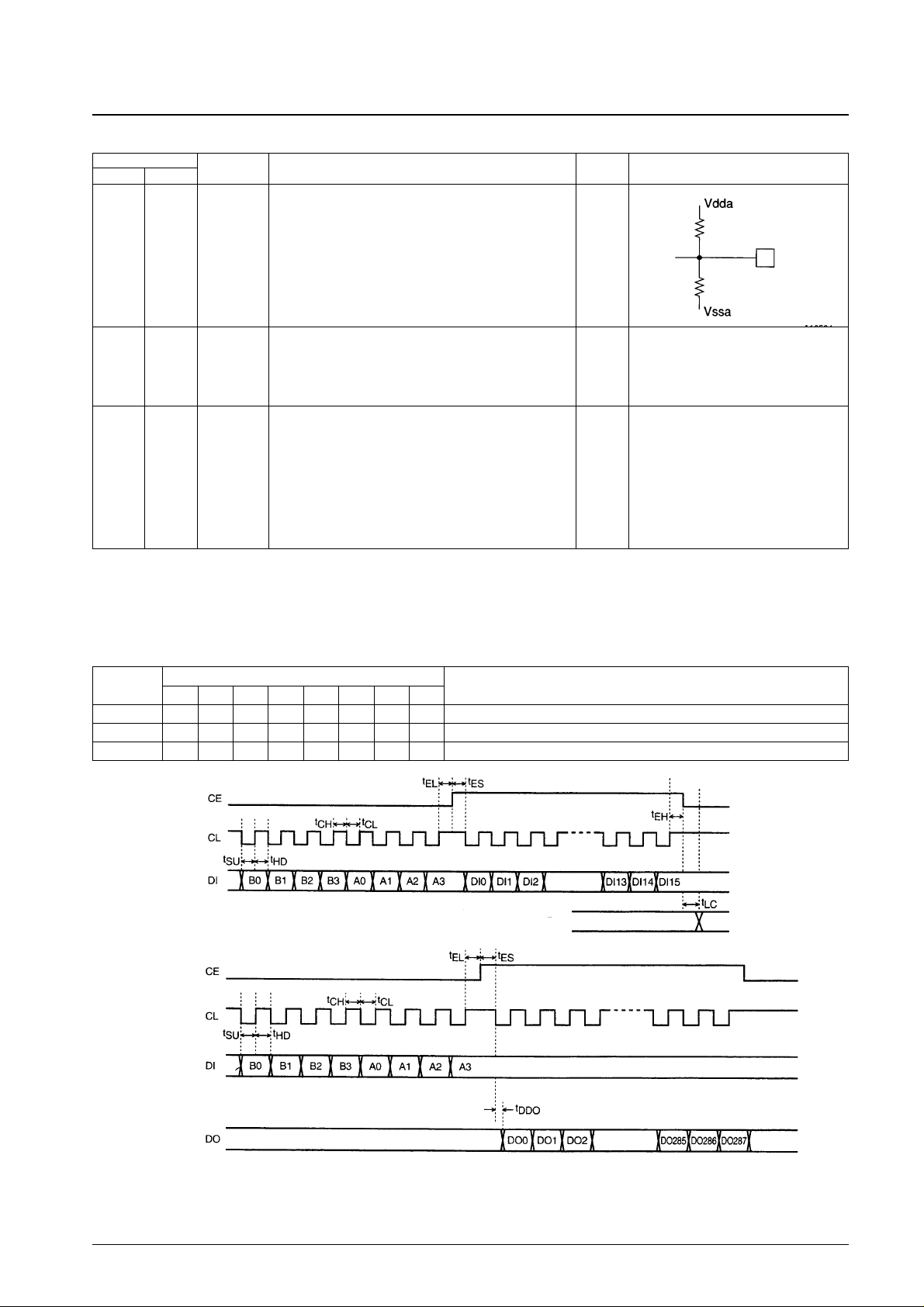
• CCB Technique
Sanyo audio ICs input and output data using the Sanyo CCB (computer control bus) standard, which is a serial bus
format. This IC uses an 8-bit address CCB and uses the following addresses.
• Data Input Timing
I/O mode
Address
Function
B0 B1 B2 B3 A0 A1 A2 A3
Input 0 1 0 1 1 1 1 1 16-bit control data input
Output 1 1 0 1 1 1 1 1 Data output for the input clock (CL)
Input 0 0 1 1 1 1 1 1 Data input (in 8-bit units) for the layer 4 CRC check circuit
Internal data latching
A10595
• Data Output Timing
A10596
Note:The DO pin is normally left open.
Since the DO pin is an n-channel open drain pin, the time required for the data to change from the low level to the high level depends on the value of
the pull-up resistor.
 Loading...