

SANYO Electric Co.,Ltd. Semiconductor Bussiness Headquarters
TOKYO OFFICE Tokyo Bldg., 1-10, 1 Chome, Ueno, Taito-ku, TOKYO, 110 JAPAN
Overview
The LC72700E and LC72700G are data decoder LSIs for
receiving DARCTMmobile FM multiplex broadcasts. A
multi-function, compact, adjustment-free system can be
implemented in two chips by combining this LSI with the
LV3400M band-pass filter IC, which extracts the
multiplex components from a composite FM signal.
Functions and Features
• Delay detection scheme using a 1T delay
• Built-in error correction function using a 2T delay
• Digital PLL clock regeneration
• Block and frame synchronization detection with a
settable synchronization protection count
• Settable block identifier code (BIC) detection precision
• Error correction using (272,190) codes
• Built-in frame memory for product codes
• Support for both serial and parallel data I/O
• Package
LC72700E: QFP48E
LC72700G: QFP48G
CMOS LSI
Ordering number : EN4870E
63097HA (OT)/D3095HA (OT)/D1594TH (OT) No.4870-1/14
SANYO: QFP48E
[LC72700E]
SANYO: QFP48G
[LC72700G]
SANYO Electric Co.,Ltd. Semiconductor Bussiness Headquarters
TOKYO OFFICE Tokyo Bldg., 1-10, 1 Chome, Ueno, Taito-ku, TOKYO, 110 JAPAN
Mobile FM Multiplex Broadcast Receiver LSI
LC72700E, LC72700G
Specifications
Absolute Maximum Ratings at Ta = 25°C
Parameter Symbol Conditions Ratings Unit
Maximum supply voltage V
DD
max V
DD
–0.3 to +7.0 V
Input voltage
V
IN
1 CL, CE, and DI pins –0.3 to +7.0 V
V
IN
2 Input pins other than VIN1 –0.3 to VDD+ 0.3 V
Output voltage
V
OUT
1 DO pin –0.3 to +7.0 V
V
OUT
2 Output pins other than V
OUT
1 –0.3 to VDD+ 0.3 V
Output current I
OUT
BCLOCK, FCLOCK, and DO pins 0 to 4.0 mA
Allowable power dissipation Pd max Ta ≤ 85°C 400 mW
Operating temperature Topr –40 to +85 °C
Storage temperature Tstg –55 to +125 °C
Package Dimensions
unit: mm
3156-QFP48E
unit: mm
3229-QFP48G
• CCB is a trademark of SANYO ELECTRIC CO., LTD.
• CCB is SANYO’s original bus format and all the bus
addresses are controlled by SANYO.
Allowable Operating Ranges at Ta = –40 to +85°C, VSS= 0 V
Note: 1. This LSI operates at a frequency of 7.2 MHz ±250 ppm.
2. See the parallel data timing.
3. See the parallel data timing.
Electrical Characteristics in the Allowable Operating Ranges
No. 4870-2/14
LC72700E, LC72700G
Parameter Symbol Conditions min typ max Unit
Supply voltage V
DD
V
DD
4.5 5.0 5.5 V
V
IH
1
MSK, DAT0 to 7, RE, PST, S/P, PORT0 to 2, RST,
0.7 V
DD
V
DD
V
Input high level voltage
TEST1, TEST2
V
IH
2 CL, CE, DI 0.7 V
DD
5.5 V
V
IL
1
MSK, DAT0 to 7, RE, PST, S/P, PORT0 to 2, RST,
V
SS
0.3 V
DD
V
Input low level voltage
TEST1, TEST2
V
IL
2 CL, CE, DI V
SS
0.3 V
DD
V
Oscillator frequency F
OSC
*
1
7.2 MHz
Input sensitivity V
XI
XIN, sine wave, capacitive coupling 400 1500 mVrms
Serial I/O
*2
Clock low level time t
CL
CL 0.7 µs
Clock high level time t
CH
CL 0.7 µs
Data setup time t
SU
CL, DI 0.7 µs
Data hold time t
HD
CL, DI 0.7 µs
CE wait time t
EL
CL, CE 0.7 µs
CE setup time t
ES
CL, CE 0.7 µs
CE hold time t
EH
CL, CE 0.7 µs
Data latch switching time t
LC
0.7 µs
Data output time t
DDO
DO, CE 277 555 ns
Parallel I/O
*3
RE wait time t
RE
RE 1 µs
RDY wait time t
DRD
RE, RDY 0.5 0.8 µs
RDY output time t
RDY
RDY 2.2 µs
PST input time t
PS
PST 0.3 µs
PST hold time t
PH
PST, DAT0 to 7, PORT0 to 2 10 ns
I/O direction switching time
t
DIR
PST, DAT0 to 7 0.5 0.8 µs
Parameter Symbol Conditions min typ max Unit
V
OH
1 IO= 1 mA, FILCK, CLK, DATA VDD– 1.0 V
High level output voltage
V
OH
2
I
O
= 2 mA, DAT0 to 7, BCLOCK, FCLOCK, BL-CK,
V
DD
– 0.4 V
FC-CK, INT-R, RDY, RDY0
Low level output voltage
V
OL
1 IO= 1 mA, for the VOH1 applicable pins 1.0 V
V
OL
2 IO= 2 mA, for the VOH2 applicable pins 0.4 V
V
OL
3 IO= 2 mA, DO 0.4 V
I
IH
1 VIN= 5.5 V, CE, CL, DI 1 µA
High level input current
I
IH
2 VIN= VDD, input pins except IIH1 1 µA
I
IL
1 VIN= VSS, CE, CL, DI –1 µA
Low level input current
I
IL
2
V
IN
= VSS, inputs with pull-up resistors, RE, PST,
–100 µA
PORT0 to 2, S/P
I
IL
3 V
IN
= V
SS,
MSK, RST –1 µA
Output off leakage current I
OFF
VO= V
DD,
DO 5 µA
Hysteresis voltage V
HIS
MSK, CL, CE, DI, RST 0.1 V
DD
V
Built-in feedback resistance Rf XIN, XOUT 1.0 MΩ
Pull-up resistance Rpu RE, PST, PORT0 to 2, S/P 50 kΩ
Current drain I
DD
16 25 mA
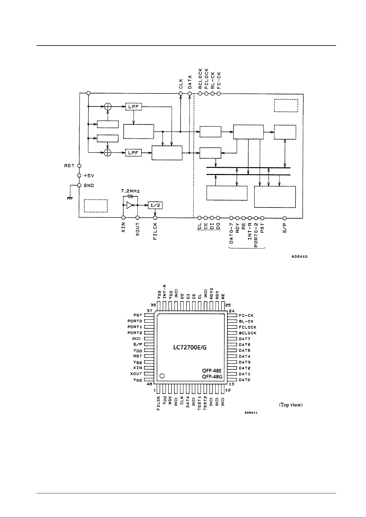
Block Diagram
Pin Assignment
No. 4870-3/14
LC72700E, LC72700G
MSK signal
input
1T delay
2T delay
Clock
regeneration
Demodulation
block
Synchronization
regeneration
PN
decoding
Timing
control
Output control
(CPU interface)
Memory cell
Error
correction
block
Error
correction
MSK error
correction
Data
Address
(Parallel I/O)
(Serial I/O)
Pin Descriptions
No. 4870-4/14
LC72700E, LC72700G
Pin No. Symbol Function I/O I/O Circuit
3
29
30
31
1
5
6
21
22
23
24
26
27
35
13
14
15
16
17
18
19
20
32
46
47
2, 34, 43
36, 45, 48
4, 7, 10
11, 12, 28
33, 41
MSK
CL
CE
DI
FILCK
CLK
DATA
BCLOCK
FCLOCK
BL-CK
FC-CK
RDY
RDY0
INT-R
DAT0
DAT1
DAT2
DAT3
DAT4
DAT5
DAT6
DAT7
DO
XIN
XOUT
V
DD
V
SS
NC
76 kHz MSK signal input
CCB serial interface Clock input
Data control input
Data input
Reference clock output for the LV3400M
Clock regeneration monitor output
Demodulated data monitor output
Outputs a high level during block synchronization
Outputs a high level during frame synchronization
Block start signal output
Frame start signal output
Parallel IF data output enable signal
Parallel IF data output enable signal
Output data external CPU interrupt signal
Parallel IF data output pin 0
Parallel IF data output pin 1
Parallel IF data output pin 2
Parallel IF data output pin 3
Parallel IF data output pin 4
Parallel IF data output pin 5
Parallel IF data output pin 6
Parallel IF data output pin 7
CCB serial interface data output
System clock oscillator crystal connection
Power supply (+4.5 to +5.5 V)
Ground pin
Not connected
Output
I/O
Output
Input
Output
—
—
—
Input
44
8
9
RST
TEST1
TEST2
System reset input pin (negative logic)
Test pin 1 (normally connected to ground)
Test pin 2 (normally connected to ground)
37
38
39
40
PST
PORT0
PORT1
PORT2
Parallel IF mode data settings
Port address 0
Port address 1
Port address 2
Input
42
S/P
Serial/parallel IF switch
(Serial mode when high)
25
RE Parallel IF mode data output control signal input
Input
A02414
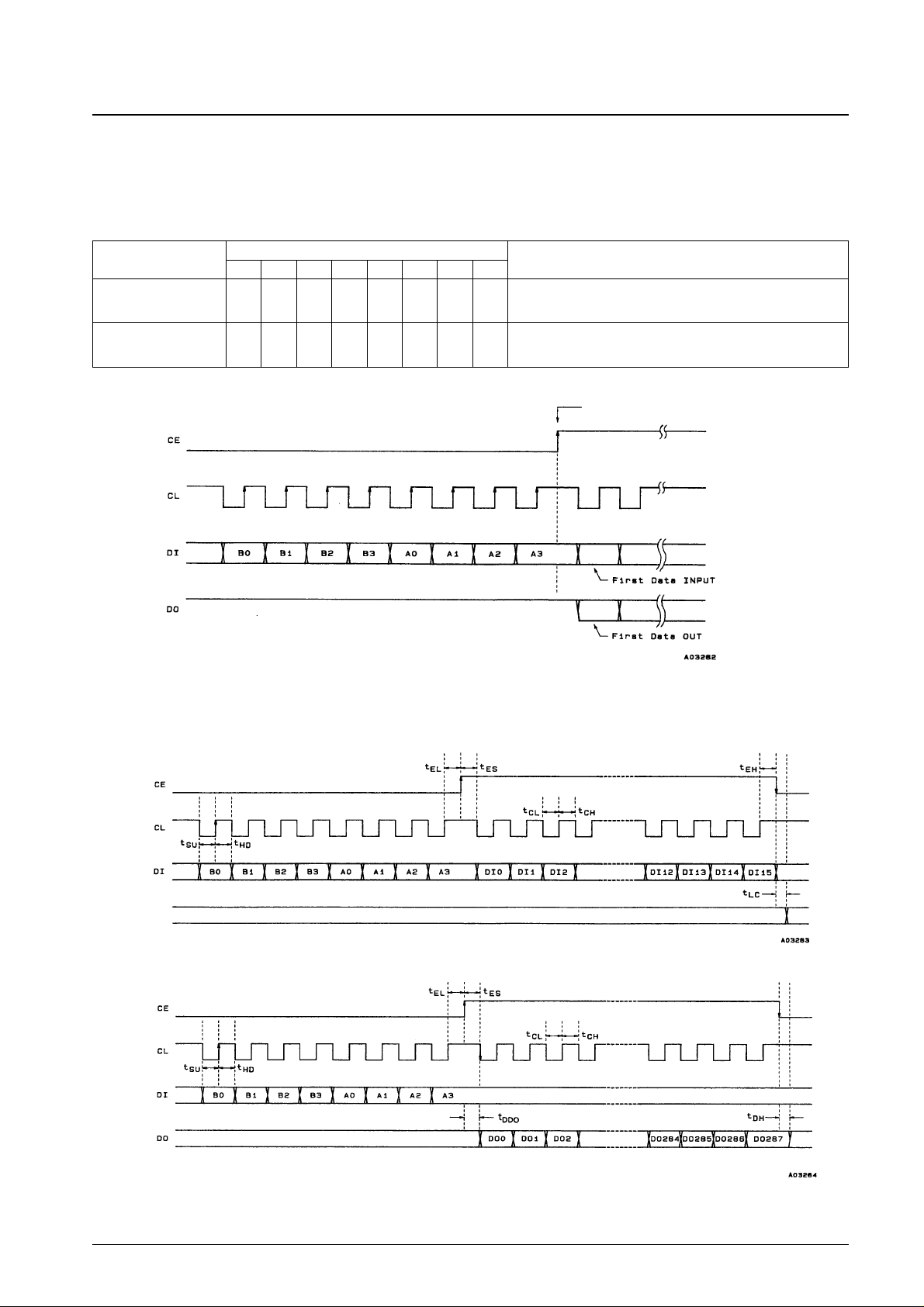
Serial Data I/O Scheme
1. CCB Format
The figure shows the Sanyo audio LSI serial bus format. Data is input and output over a CCB (computer control
bus). This LSI uses an 8-bit address CCB format.
2. Serial Data Input Timing
3. Serial Data Output Timing
Note: * The DO pin is normally open.
Since the DO pin is an n-channel open-drain output, the time for the data value to change from the low level to the high level depends on the value
of the pull-up resistor used.
No. 4870-5/14
LC72700E, LC72700G
I/O mode
Address
Function
B0 B1 B2 B3 A0 A1 A2 A3
Input
Output
0 1 0 1 1 1 1 1
1 1 0 1 1 1 1 1
16-bit control data input
Data output
Internal data
I/O mode is set.
 Loading...