

SANYO LC723764, LC723756, LC723740, LC723732, LC723748 Datasheet

Overview
The LC723700 Series are large-capacity ETR
microcontrollers that achieve an instruction execution time
of 1.33 µ s and provide up to 64 KB of ROM and up to
2 KB of RAM. They include an on-chip high-performance
PLL circuit that features an added high-speed lock circuit
and can control the C/N characteristics of a local
oscillator. They also provide a rich set of on-chip interface
circuits, including a 3-channel serial I/O port, and an 8input 8-bit A/D converter.
Functions
• ROM
— Up to 32K steps (32,767 × 16 bits)
— The subroutine area holds 4 K steps (4,096 × 16 bits)
• RAM
— Up to 4 K × 4 bits (In banks 00 through 3F)
LC723732 – ROM: 32 KB, RAM 1 KB
LC723740 – ROM: 40 KB, RAM 2 KB
LC723748 – ROM: 48 KB, RAM 2 KB
LC723756 – ROM: 56 KB, RAM 2 KB
LC723764 – ROM: 64 KB, RAM 2 KB
• Stack
— 32 levels
• Serial I/O
— Three channels. These circuits can support both 2-
wire and 3-wire 8-bit communication techniques,
and can be switched between MSB first and LSB
first operation.
— One of six internally generated serial transfer clock
rates can be selected: 12.5, 37.5, 187.5, 281.25, 375,
and 450 kHz.
• External interrupts
— Seven interrupt inputs (pins INT0 through INT5, and
the HOLD pin)
These interrupts can be set to switch between rising
and falling edges, although the HOLD pin only
supports falling edge detection.
• Internal interrupts
— Seven interrupts; four internal timer interrupts, and
three serial I/O interrupts.
• Interrupt nesting levels
— 16 levels
— Interrupt are prioritized in hardware as follows:
HOLD pin > INT0 pin > INT1 pin > INT2 pin >
INT3 pin > INT4 pin > INT5 pin > S-I/O0 > S-I/O1
> S-I/O2 > internal TMR0 > internal TMR1 >
internal TMR2 > internal TMR3
• A/D converter
— 8-bit resolution and 8 inputs
• General-purpose ports
— Input ports: 12
— Output ports : 4
— I/O ports: 62 (These pins can be switched between
input and output in 1-bit units.)
• PLL block
— Includes a sub-charge pump for high-speed locking.
— Supports dead zone control.
— Built-in unlock detection circuit.
— Twelve reference frequencies: 1, 3, 3.125, 5, 6.25, 9,
10, 12.5, 25, 30, 50, and 100 kHz.
— A second PLL circuit is also included for use in AM
up conversion.
• Universal counter
— This 20-bit counter can be used for either frequency
or period measurement and supports four
measurement (calculation) periods: 1, 4, 8, and 32 ms.
• Timers
— Two fixed timers and two programmable timers (8-
bit counters)
TMR0: Supports four periods: 10 µ s, 100 µs, 1 ms,
and 5 ms
TMR1: Supports four periods: 10 µ s, 100 µs, 1 ms,
and 10 ms
TMR2 and TMR3: Programmable 8-bit counters.
Input clocks with 10 µ s, 100 µs, and 1 ms periods
are provided.
— One 125-ms timer flip-flop provided.
• Beep circuit
— Provides 12 fixed beep tones: 0.5, 1, 2, 2.08, 2.2,
2.5, 3.33, 3.75, 4.17, and 7.03 kHz.
— Programmable 8-bit beep tone generator. Reference
clocks with frequencies of 5 kHz, 15 kHz, and 50
kHz are provided.
• Reset
— Built-in voltage detection reset circuit
— External reset pin
CMOS IC
51398RM (OT) No.5931-1/14
SANYO Electric Co.,Ltd. Semiconductor Bussiness Headquarters
TOKYO OFFICE Tokyo Bldg., 1-10, 1 Chome, Ueno, Taito-ku, TOKYO, 110-8534 JAPAN
ETR Microcontrollers
LC723732/40/48/56/64
Ordering number : EN5931
• Cycle time
— 1.33 µs (All instructions are one word.)
• Halt mode
— The microcontroller operating clock is stopped in
halt mode.
There are four conditions that can clear halt mode: an
interrupt request, a timer flip-flop overflow, a PA
port input, or a HOLD pin input.
• Operating supply voltage
— 4.5 to 5.5 V (Microcontroller block only: 3.5 to 5.5
V)
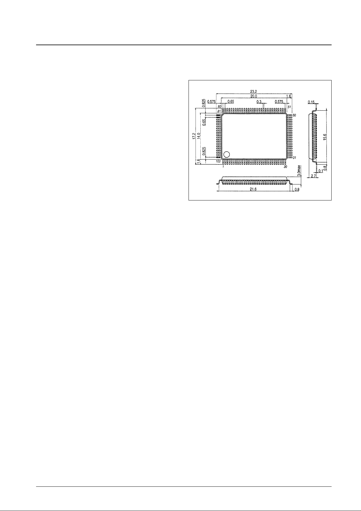
• Package
— QIP100E
• OTP version
— LC72P3700
• Development tools
— Emulator :RE32N
— Evaluation chip: LC72EV3700
— Evaluation chip board: EB-72EV3700
Package Dimensions
unit: mm
3151-QFP100E
No. 5931-2/14
LC723732/40/48/56/64
SANYO: QFP100E
[LC723732/40/48/56/64]
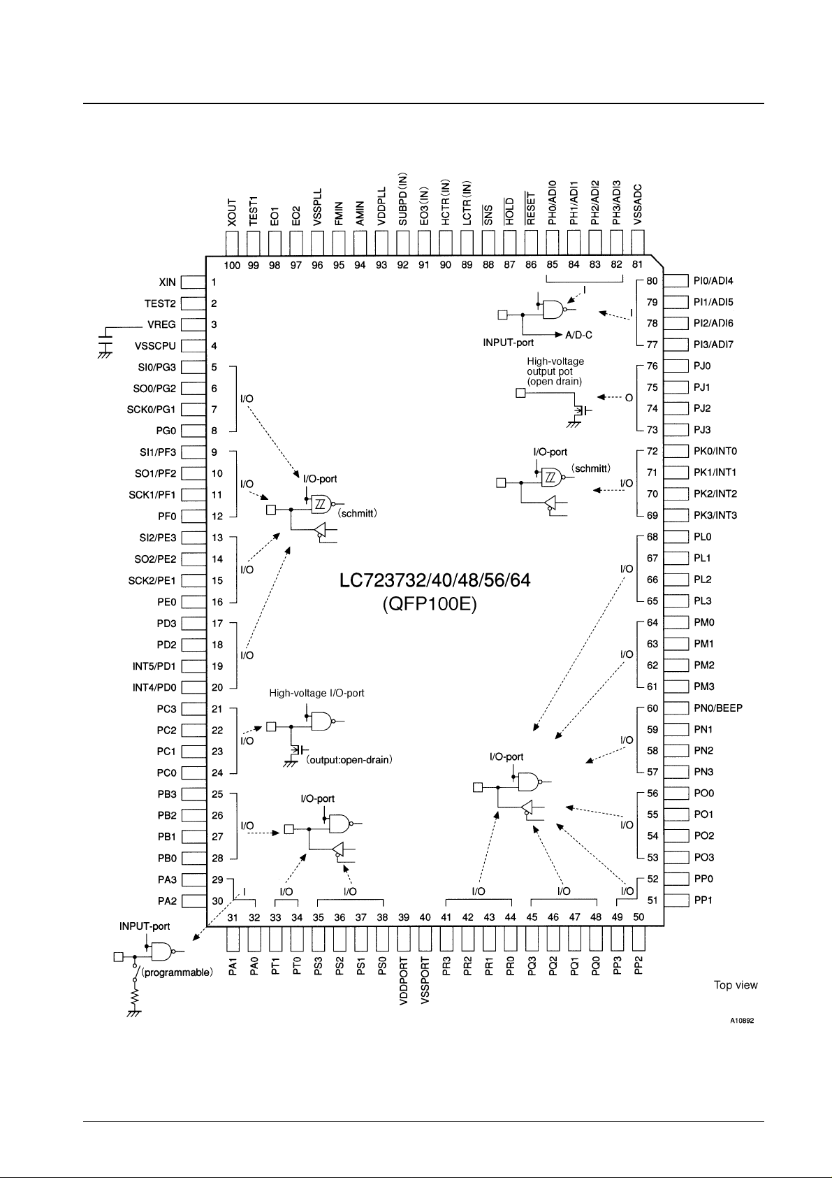
Pin Assignment
No. 5931-3/14
LC723732/40/48/56/64
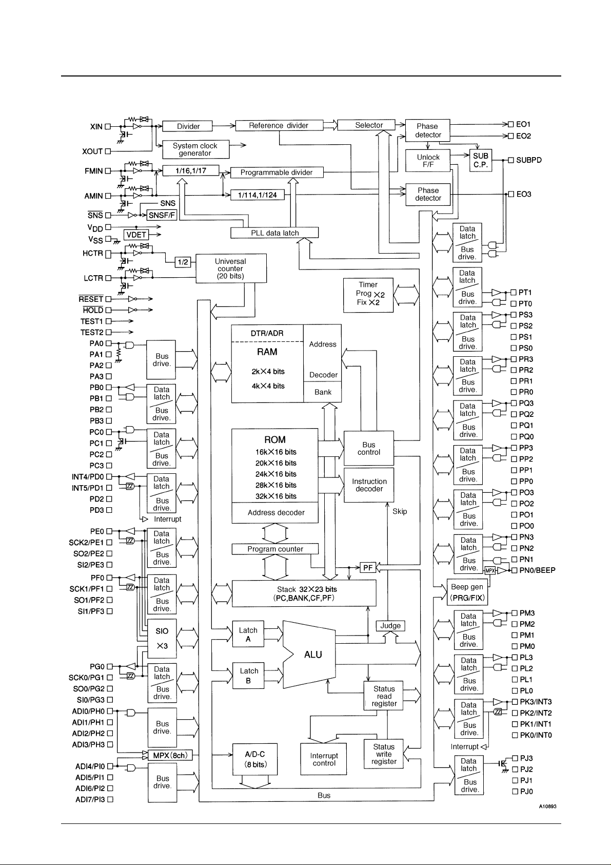
Block Diagram
No. 5931-4/14
LC723732/40/48/56/64
No. 5931-5/14
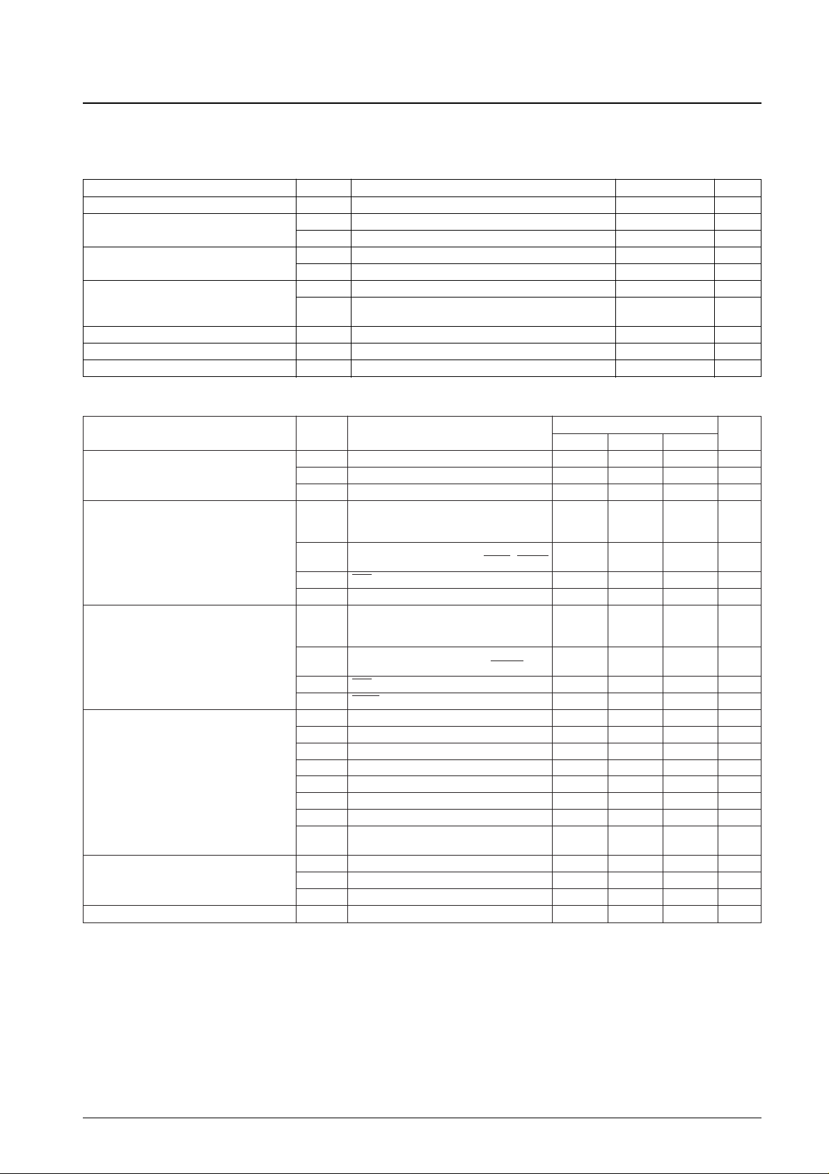
LC723732/40/48/56/64
Parameter Symbol Conditions Ratings Unit
Maximum supply voltage V
DD
max –0.3 to +6.5 V
Input voltage
V
IN
1 PC-PORT –0.3 to +15 V
V
IN
2 All input pins other than VIN1 –0.3 to VDD+ 0.3 V
Output voltage
V
OUT
1 PC, PJ-PORT –0.3 to +15 V
V
OUT
2 All output pins other than V
OUT
1 –0.3 to VDD+ 0.3 V
I
OUT
1 PC, PJ-PORT 0 to +5 mA
Output current
I
OUT
2
PB, PD, PE, PF, PG, PK, PL, PM, PN, PO, PP, PQ, PR,
0 to +3 mA
PS, PT, PT-PORT, EO1, EO2, EO3, SUBPD
Allowable power dissipation Pd max Ta = –40 to +85°C 400 mW
Operating temperature Topg –40 to +85 °C
Storage temperature Tstg –45 to +125 °C
Specifications
Electrical Characteristics
Absolute Maximum Ratings at Ta = 25°C, VSS= 0 V
Parameter Symbol Conditions
Ratings
Unit
min typ max
V
DD
1 CPU and PLL operating 4.5 5.0 5.5 V
Supply voltage V
DD
2 CPU operating 3.5 5.5 V
V
DD
3 Memory retention 1.3 5.5 V
PB, PC, PH, PI, PL, PM, PN, PO, PP, PQ, PR,
VIH1 PS, PT-PORT, HCTR, LCTR, E03, SUBPD 0.7 V
DD
V
DD
V
(with the I/O ports set to input mode.)
Input high-level voltage
V
IH
2
PD, PE, PF, PG, PK-PORT, LCTR,
0.8 V
DD
V
DD
V
(in period measurement mode)
, HOLD, RESET
V
IH
3 SNS 2.5 V
DD
V
V
IH
4 PA-PORT 0.6 V
DD
V
DD
V
PB, PC, PH, PI, PL, PM, PN, PO, PP, PQ, PR,
VIL1 PS, PT-PORT, HCTR, LCTR, E03, SUBPD 0 0.3 V
DD
V
(with the I/O ports set to input mode.)
Input low-level voltage V
IL
2
PA, PD, PE, PF, PG, PK-PORT, LCTR
0 0.2 V
DD
V
(in period measurement mode), RESET
V
IL
3 SNS 0 1.3 V
V
IL
4 HOLD 0 0.4 V
DD
V
f
IN
1 XIN 4.0 4.5 5.0 MHz
f
IN
2 FMIN VIN2, VDD1 10 150 MHz
f
IN
3 FMIN VIN3, VDD1 10 130 MHz
f
IN
4 AMIN(H) VIN3, VDD1 2.0 40 MHz
Input frequency f
IN
5 AMIN(L) VIN3, VDD1 0.5 10 MHz
f
IN
6 HCTR VIN3, VDD1 0.4 12 MHz
f
IN
7 LCTR VIN3, VDD1 100 500 kHz
f
IN
8
LCTR(period measurement)
1 20 × 10
3
Hz
V
IH
2, VIL2, VDD1
V
IN
1 XIN 0.5 1.5 Vrms
Input amplitude V
IN
2 FMIN 0.07 1.5 Vrms
V
IN
3 FMIN, AMIN, HCTR, LCTR 0.04 1.5 Vrms
Input voltage range V
IN
4 ADI0 to ADI7 0 V
DD
V
Allowable Operating Ranges at Ta = –40 to +85°C, VDD= 3.5 to 5.5 V
 Loading...