

Sanyo LC72135M Specifications
Any and all SANYO products described or contained herein do not have specifications that can handle
applications that require extremely high levels of reliability, such as life-support systems, aircraft’s
control systems, or other applications whose failure can be reasonably expected to result in serious
physical and/or material damage. Consult with your SANYO representative nearest you before using
any SANYO products described or contained herein in such applications.
SANYO assumes no responsibility for equipment failures that result from using products at values that
exceed, even momentarily, rated values (such as maximum ratings, operating condition ranges, or other
parameters) listed in products specifications of any and all SANYO products described or contained
herein.
83098HA (OT)/22896HA (OT) No. 5175-1/24
SANYO Electric Co.,Ltd. Semiconductor Bussiness Headquarters
TOKYO OFFICE Tokyo Bldg., 1-10, 1 Chome, Ueno, Taito-ku, TOKYO, 110-8534 JAPAN
Overview
The LC72135M is a PLL frequency synthesizer LSI for
tuners in car stereo and similar applications. Highperformance AM/FM tuners can be easily implemented
with this product.
Functions
• High-speed programmable dividers
— FMIN: 10 to 160 MHz..........pulse swallower
(built-in divide-by-two prescaler)
— AMIN: 2 to 40 MHz..............pulse swallower
0.5 to 10 MHz...........direct division
• IF counter
— HCTR 0.4 to 12 MHz...........AM/FM IF counter
— LCTR 100 to 500 k Hz.........AM IF counter
• Reference frequencies
— Twelve selectable frequencies
(4.5 or 7.2 MHz crystal)
1, 3, 5, 9, 10, 3.125, 6.25, 12.5, 15, 25, 50 and 100 kHz
• Phase comparator
— Dead zone control
— Unlock detection circuit
— Deadlock clear circuit
• Built-in MOS transistor for forming an active low-pass
filter
• I/O ports
— Dedicated output ports: 4
— Input or output ports: 1
— Input ports (LCTR) : 1
— Support clock time base output
• Serial data I/O
— Support CCB format communication with the
system controller.
• Operating ranges
— Supply voltage........................4.5 to 5.5 V
— Operating temperature............–40 to +85°C
• Package
— MFP20
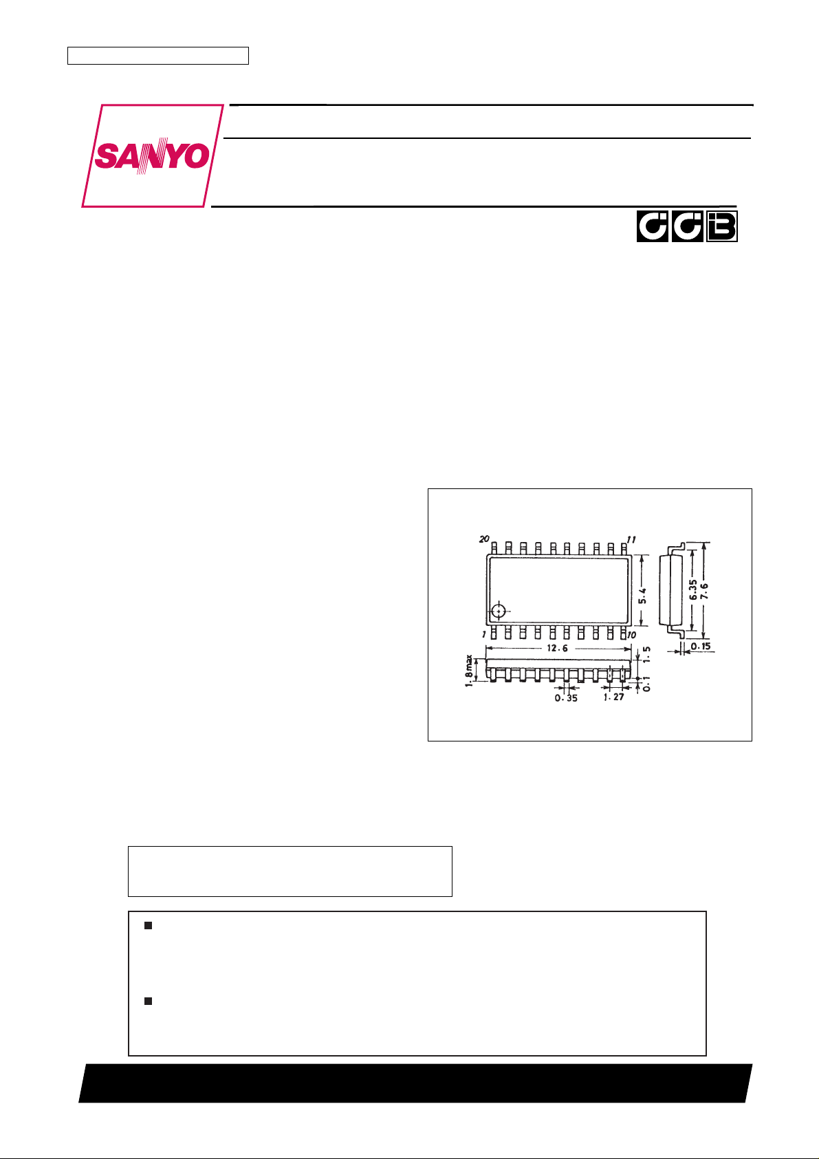
Package Dimensions
unit: mm
3036B-MFP20
SANYO: MFP20
[LC72135M]
• CCB is a trademark of SANYO ELECTRIC CO., LTD.
• CCB is SANYO’s original bus format and all the bus
addresses are controlled by SANYO.
CMOS LSI
Ordering number : EN5175A
LC72135M
PLL Frequency Synthesizer for Electronic
Tuning
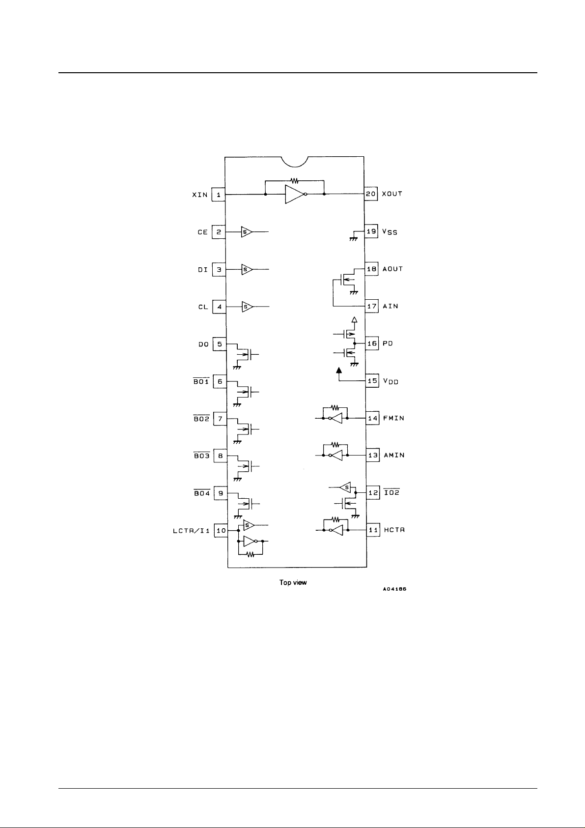
Pin Assignment
No. 5175-2/24
LC72135M
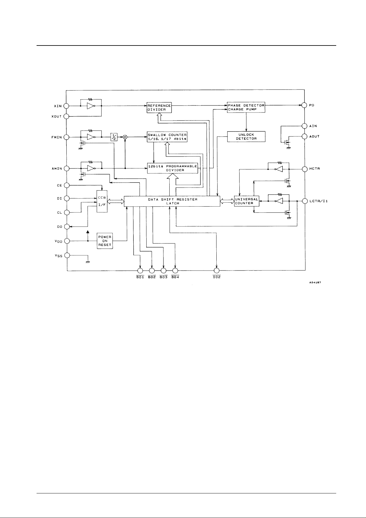
Block Diagram
No. 5175-3/24
LC72135M
Specifications
Absolute Maximum Ratings at Ta = 25°C, VSS= 0 V
Allowable Operating Ranges at Ta = –40 to +85°C, VSS= 0 V
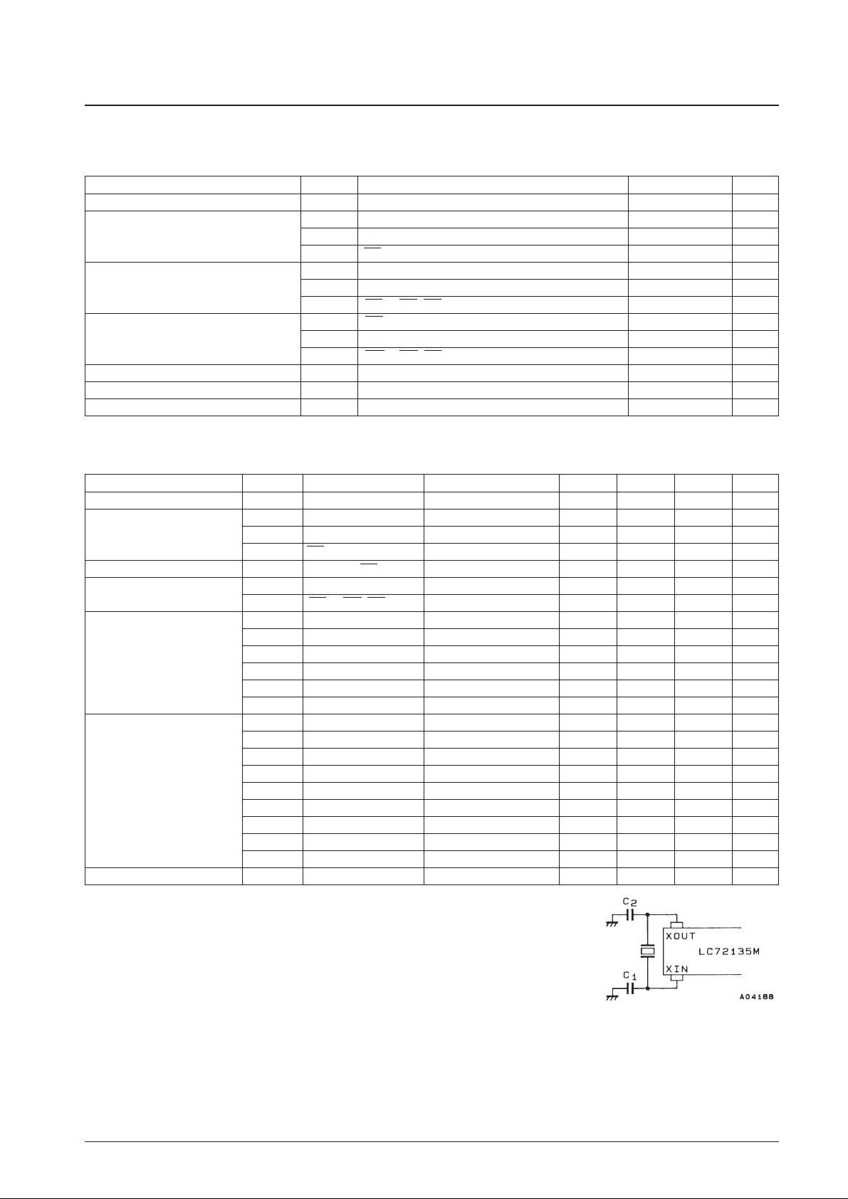
Note: * Recommended crystal oscillator CI values:
CI ≤ 120Ω (For a 4.5 MHz crystal)
CI ≤ 70Ω (For a 7.2 MHz crystal)
<Sample Oscillator Circuit>
Crystal oscillator: HC-49/U (manufactured by Kinseki, Ltd.), CL = 12 pF
C1 = C2 = 15 pF
The circuit constants for the crystal oscillator circuit depend on the crystal used, the printed circuit
board pattern, and other items. Therefore we recommend consulting with the manufacturer of the
crystal about evaluation and reliability.
No. 5175-4/24
LC72135M
Parameter Symbol Pins Ratings Unit
Maximum supply voltage V
DD
max V
DD
–0.3 to +7.0 V
V
IN
1 max CE, CL, DI, AIN –0.3 to +7.0 V
Maximum input voltage V
IN
2 max XIN, FMIN, AMIN, HCTR, LCTR/I1 –0.3 to VDD+ 0.3 V
V
IN
3 max IO2 –0.3 to +15 V
V
O
1 max DO –0.3 to +7.0 V
Maximum output voltage V
O
2 max XOUT, PD –0.3 to VDD+ 0.3 V
V
O
3 max BO1 to BO4, IO2, AOUT –0.3 to +15 V
I
O
1 max BO1 0 to 3.0 mA
Maximum output current I
O
2 max AOUT, DO 0 to 6.0 mA
I
O
3 max BO2 to BO4, IO2 0 to 10.0 mA
Allowable power dissipation Pd max Ta ≤ 85°C 180 mW
Operating temperature Topr –40 to +85 °C
Storage temperature Tstg –55 to +125 °C
Parameter Symbol Pins Conditions min typ max Unit
Supply voltage V
DD
V
DD
4.5 5.5 V
V
IH
1 CE, CL, DI 0.7 V
DD
6.5 V
Input high-level voltage V
IH
2 LCTR/I1 0.7 V
DD
V
DD
V
V
IH
3 IO2 0.7 V
DD
13 V
Input low-level voltage V
IL
CE, CL, DI, IO2, LCTR/I1 0 0.3 V
DD
V
V
O
1 DO 0 +6.5 V
Output voltage
V
O
2 BO1 to BO4, IO2, AOUT 0 +13 V
f
IN
1 XIN VIN1 1 8 MHz
f
IN
2 FMIN VIN2 10 160 MHz
Input frequency
f
IN
3 AMIN VIN3, SNS = 1 2 40 MHz
f
IN
4 AMIN VIN4, SNS = 0 0.5 10 MHz
f
IN
5 HCTR VIN5 0.4 12 MHz
f
IN
6 LCTR/I1 VIN6 100 500 kHz
V
IN
1 XIN fIN1 400 1500 mVrms
V
IN
2-1 FMIN f = 10 to 130 MHz 40 1500 mVrms
V
IN
2-2 FMIN f = 130 to 160 MHz 70 1500 mVrms
V
IN
3 AMIN fIN3, SNS = 1 40 1500 mVrms
Input amplitude V
IN
4 AMIN fIN4, SNS = 0 40 1500 mVrms
V
IN
5-1 HCTR fIN5, IFS = 1 40 1500 mVrms
V
IN
5-2 HCTR fIN5, IFS = 0 70 1500 mVrms
V
IN
6-1 LCTR/I1 fIN6, IFS = 1 40 1500 mVrms
V
IN
6-2 LCTR/I1 fIN6, IFS = 0 70 1500 mVrms
Supported crystals Xtal XIN, XOUT * 4.0 8.0 MHz
Electrical Characteristics for the Allowable Operating Ranges at Ta = –40 to +85°C, VSS= 0 V
No. 5175-5/24
LC72135M
Parameter Symbol Pins Conditions min typ max Unit
Rf1 XIN 1.0 MΩ
Built-in feedback resistance
Rf2 FMIN 500 kΩ
Rf3 AMIN 500 kΩ
Rf4 HCTR 250 kΩ
Rf5 LCTR/I1 250 kΩ
Built-in pull-down resistor
Rpd1 FMIN 200 kΩ
Rpd2 AMIN 200 kΩ
Hysteresis V
HIS
CE, CL, DI, IO2, LCTR/I1 0.1 V
DD
V
Output high-level voltage V
OH
1 PD IO= –1 mA VDD– 1.0 V
V
OL
1 PD IO= 1 mA 1.0 V
V
OL
2 BO1
IO= 0.5 mA 0.5 V
I
O
= 1 mA 1.0 V
V
OL
3 DO
IO= 1 mA 0.2 V
Output low-level voltage I
O
= 5 mA 1.0 V
I
O
= 1 mA 0.2 V
V
OL
4 BO2 to BO4, IO2 IO= 5 mA 1.0 V
I
O
= 8 mA 1.6 V
V
OL
5 AOUT IO= 1 mA, AIN = 1.3 V 0.5 V
I
IH
1 CE, CL, DI VI= 6.5 V 5.0 V
I
IH
2 LCTR/I1 VI= V
DD,
L/I1 = 0 5.0 µA
I
IH
3 IO2 VI= 13 V 5.0 µA
Input high-level current I
IH
4 XIN VI= V
DD
2.0 11 µA
I
IH
5 FMIN, AMIN VI= V
DD
4.0 22 µA
I
IH
6 HCTR, LCTR/I1 VI= VDD, L/I1 = 1 8.0 44 µA
I
IH
7 AIN VI= 6.5 V 200 nA
I
IL
1 CE, CL, DI VI= 0 V 5.0 µA
I
IL
2 LCTR/I1 VI= 0 V, L/I1 = 0 5.0 µA
Input low-level current
I
IL
3 IO2 VI= 0 V 5.0 µA
I
IL
4 XIN VI= 0 V 2.0 11 µA
I
IL
5 FMIN, AMIN VI= 0 V 4.0 22 µA
I
IL
6 HCTR, LCTR/I1 VI= 0 V, L/I1 = 1 8.0 44 µA
I
IL
7 AIN VI= 0 V 200 nA
I
OFF
1
BO1 to BO4, AOUT,
VO= 13 V 5.0 µA
Output off leakage current
IO2
I
OFF
2 DO VO= 6.5 V 5.0 µA
High-level three-state
I
OFFH
PD VO= V
DD
0.01 200 nA
off leakage current
Low-level three-state
I
OFFL
PD VO= 0 V 0.01 200 nA
off leakage current
Input capacitance C
IN
FMIN 6 pF
Xtal = 7.2 MHz,
IDD1 V
DD
fIN2 = 130 MHz, 5 10 mA
V
IN
2 = 40 mVrms
PLL block stopped
Current drain
I
DD
2 V
DD
(PLL INHIBIT),
0.5 mA
Xtal oscillator operating
(Xtal = 7.2 MHz)
IDD3 V
DD
PLL block stopped
10 µA
Xtal oscillator stopped
Pin Functions
No. 5175-6/24
LC72135M
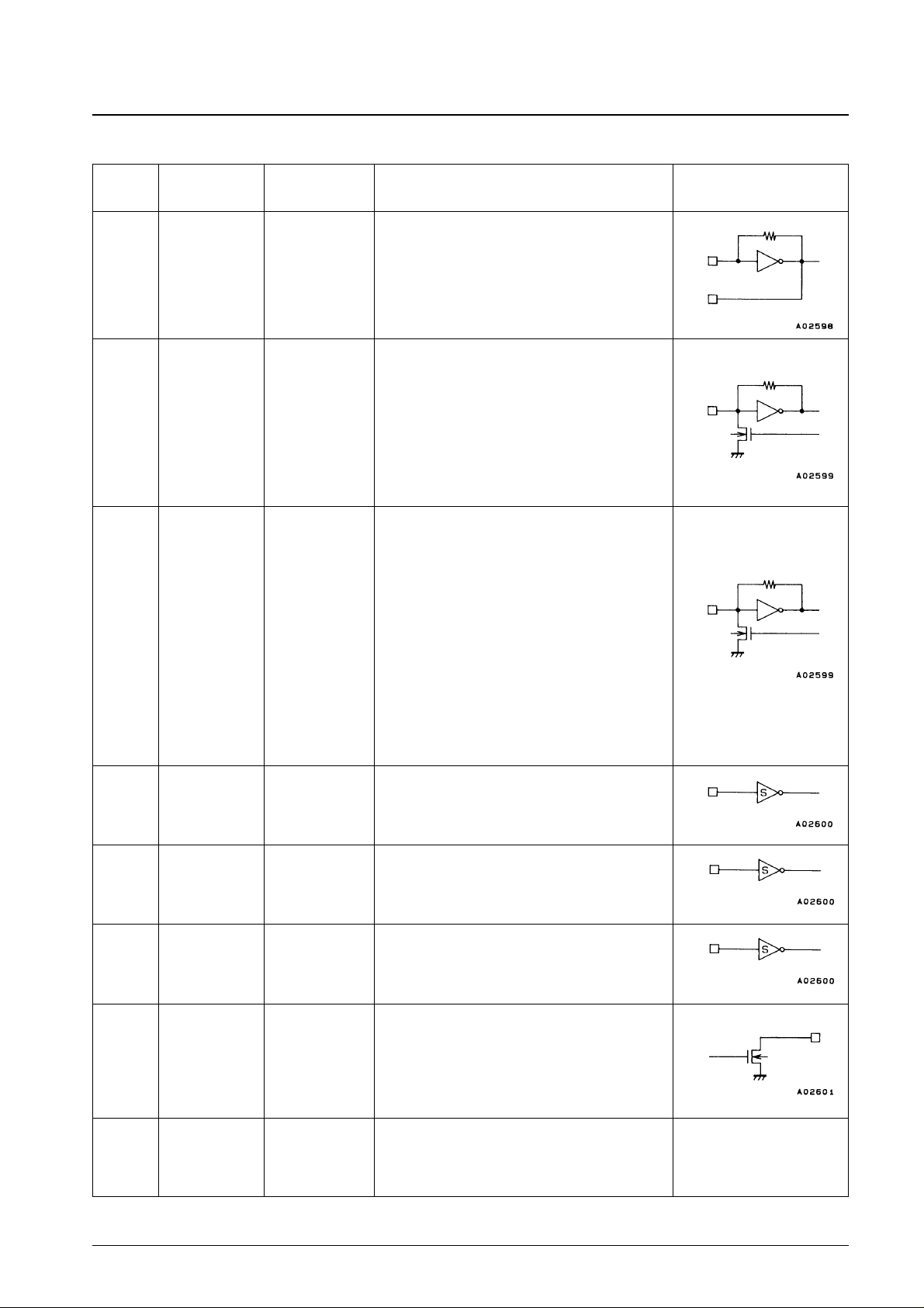
Symbol Pin No. Type Functions Circuit configuration
XIN
XOUT
FMIN
AMIN
CE
CL
DI
DO
V
DD
1
20
14
13
2
4
3
5
15
Xtal OSC
Local oscillator
signal input
Local oscillator
signal input
Chip enable
Clock
Data input
Data output
Power supply
• Crystal resonator connection
(4.5/7.2 MHz)
• FMIN is selected when the serial data input DVS bit is
set to 1.
• The input frequency range is from 10 to 160 MHz.
• The input signal passes through the internal divide-bytwo prescaler and is input to the swallow counter.
• The divisor can be in the range 272 to 65535. However,
since the signal has passed through the divide-by-two
prescaler, the actual divisor is twice the set value.
• AMIN is selected when the serial data input DVS bit is
set to 0.
• When the serial data input SNS bit is set to 1:
— The input frequency range is 2 to 40 MHz.
— The signal is directly input to the swallow counter.
— The divisor can be in the range 272 to 65535, and
the divisor used will be the value set.
• When the serial data input SNS bit is set to 0:
— The input frequency range is 0.5 to 10 MHz.
— The signal is directly input to a 12-bit programmable
divider.
— The divisor can be in the range 4 to 4095, and the
divisor used will be the value set.
Set this pin high when inputting (DI) or outputting (DO)
serial data.
• Used as the synchronization clock when inputting (DI) or
outputting (DO) serial data.
• Inputs serial data transferred from the controller to the
LC72135M.
• Outputs serial data transferred from the LC72135M to
the controller.
The content of the output data is determined by the
serial data DOC0 to DOC2.
• The LC72135M power supply pin (V
DD
= 4.5 to 5.5 V)
• The power on reset circuit operates when power is first
applied.
Continued on next page.
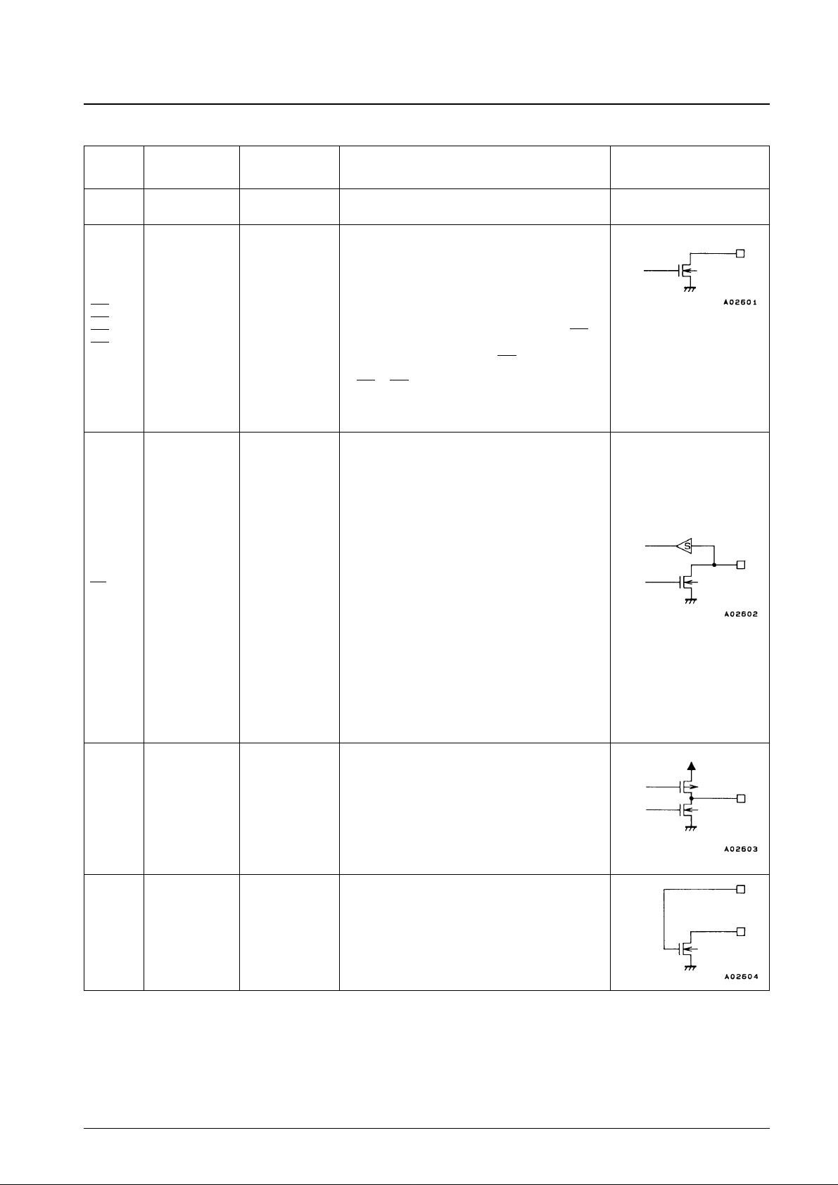
Continued from preceding page.
No. 5157-7/24
LC72135M
Symbol Pin No. Type Functions Circuit configuration
V
SS
BO1
BO2
BO3
BO4
IO2
PD
AIN
AOUT
19
6
7
8
9
12
16
17
18
Ground
Output port
I/O port
Charge pump
output
LPF amplifier
transistor
• The LC72135M ground —
• Dedicated output pins
• The output states are determined by BO1 to BO4 bits in
the serial data.
Data: 0 = open, 1 = low
• All output ports are set to the open state following a
power-on reset.
• A time base signal (8 Hz) can be output from the BO1
pin. (When the serial data TBC bit is set to 1.)
• Care is required when using the BO1 pin, since it has a
higher on impedance that the other output ports (pins
BO2 to BO4).
• I/O dual-use pins
• The direction (input or output) is determined by bit IOC2
in the serial data.
Data: 0 = input port, 1 = output port
• When specified for use as input ports:
The state of the input pin is transmitted to the controller
over the DO pin.
Input state: low = 0 data value
high = 1 data value
• When specified for use as output ports:
The output states are determined by the IO2 bit in the
serial data.
Data: 0 = open, 1 = low
• The pin function as input pin following a power-on reset.
• PLL charge pump output
When the frequency generated by dividing the local
oscillator frequency by N is higher than the reference
frequency, a high level is output from the PD pin.
Similarly, when that frequency is lower, a low level is
output. The PD pin goes to the high-impedance state
when the frequencies match.
• The n-channel MOS transistor used for the PLL active
low-pass filter.
Continued on next page.
Continued from preceding page.
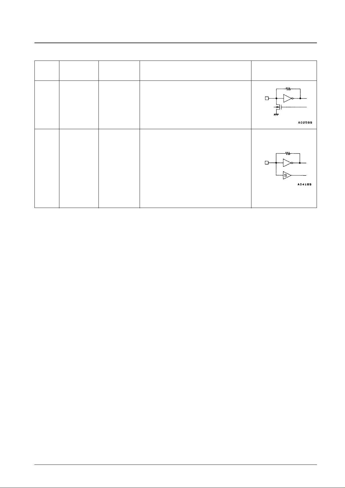
Symbol Pin No. Type Functions Circuit configuration
No. 5175-8/24
LC72135M
LCTR/I1
11
10
IF counter
IF counter
Input port
• HCTR is selected when the LCTS bit in the serial data is
set to 0.
• Accepts an input in the frequency range 0.4 to 12 MHz.
• The input signal is directly transmitted to the IF counter.
• The result is output starting the MSB of the IF counter
using the DO pin.
• Four measurement periods are supported: 4, 8, 32, and
64 ms.
• LCTR is selected when the LCTS bit in the serial data is
set to 1. (Set the L/I1 bit in the serial data to 1 when
using the IF counter.)
• The input frequency range is 100 to 500 kHz.
• The signal is directly transmitted to the IF counter.
• The result, starting with the MSB of the IF counter, is
output serially through the DO pin.
• There are four measurement times: 4, 8, 32, and 64 ms.
• If the L/I1 bit in the serial data is set to 0, the LCTR/I1 pin
functions as an input port and the state of that input pin is
transmitted to the controller from the DO pin.
• When the input state is low, the data will be 0, and when
the state is high, the data will be 1.
HCTR
 Loading...