

SANYO LC72130, LC72130M Datasheet
CMOS LSI
Ordering number : EN4973A
N3096HA (OT)/51795TH (OT) No. 4973-1/22
SANYO Electric Co.,Ltd. Semiconductor Bussiness Headquarters
TOKYO OFFICE Tokyo Bldg., 1-10, 1 Chome, Ueno, Taito-ku, TOKYO, 110 JAPAN
AM/FM PLL Frequency Synthesizer
LC72130, 72130M
Overview
The LC72130 and LC72130M are PLL frequency
synthesizers for use in tuners in radio cassette recorders
and other products.
Applications
PLL frequency synthesizer
Functions
• High-speed programmable dividers
— FMIN: 10 to 160 MHz..........pulse swallower
(built-in divide-by-two prescaler)
— AMIN: 2 to 40 MHz..............pulse swallower
0.5 to 10 MHz...........direct division
• IF counter
— IFIN: 0.4 to 12 MHz...........AM/FM IF counter
• Reference frequencies
— Twelve selectable frequencies
(4.5 or 7.2 MHz crystal)
1, 3, 5, 9, 10, 3.125, 6.25, 12.5, 15, 25, 50 and 100 kHz
• Phase comparator
— Dead zone control
— Unlock detection
— Deadlock clear circuit
• Built-in MOS transistor for implementing an active lowpass filter (two systems)
• Inputs and outputs
— Dedicated output ports: five pins
— Input or output ports: two pins
— Clock time base output available
• Serial data I/O
— Supports CCB format communication with the
system controller.
• Operating ranges
— Supply voltage........................4.5 to 5.5 V
— Operating temperature............–40 to +85°C
• Packages
— DIP24S, MFP24S
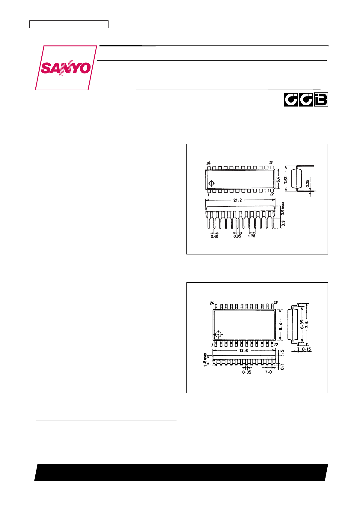
Package Dimensions
unit: mm
3067-DIP24S
unit: mm
3112-MFP24S
SANYO: DIP24S
[LC72130]
SANYO: MFP24S
[LC72130M]
• CCB is a trademark of SANYO ELECTRIC CO., LTD.
• CCB is SANYO’s original bus format and all the bus
addresses are controlled by SANYO.
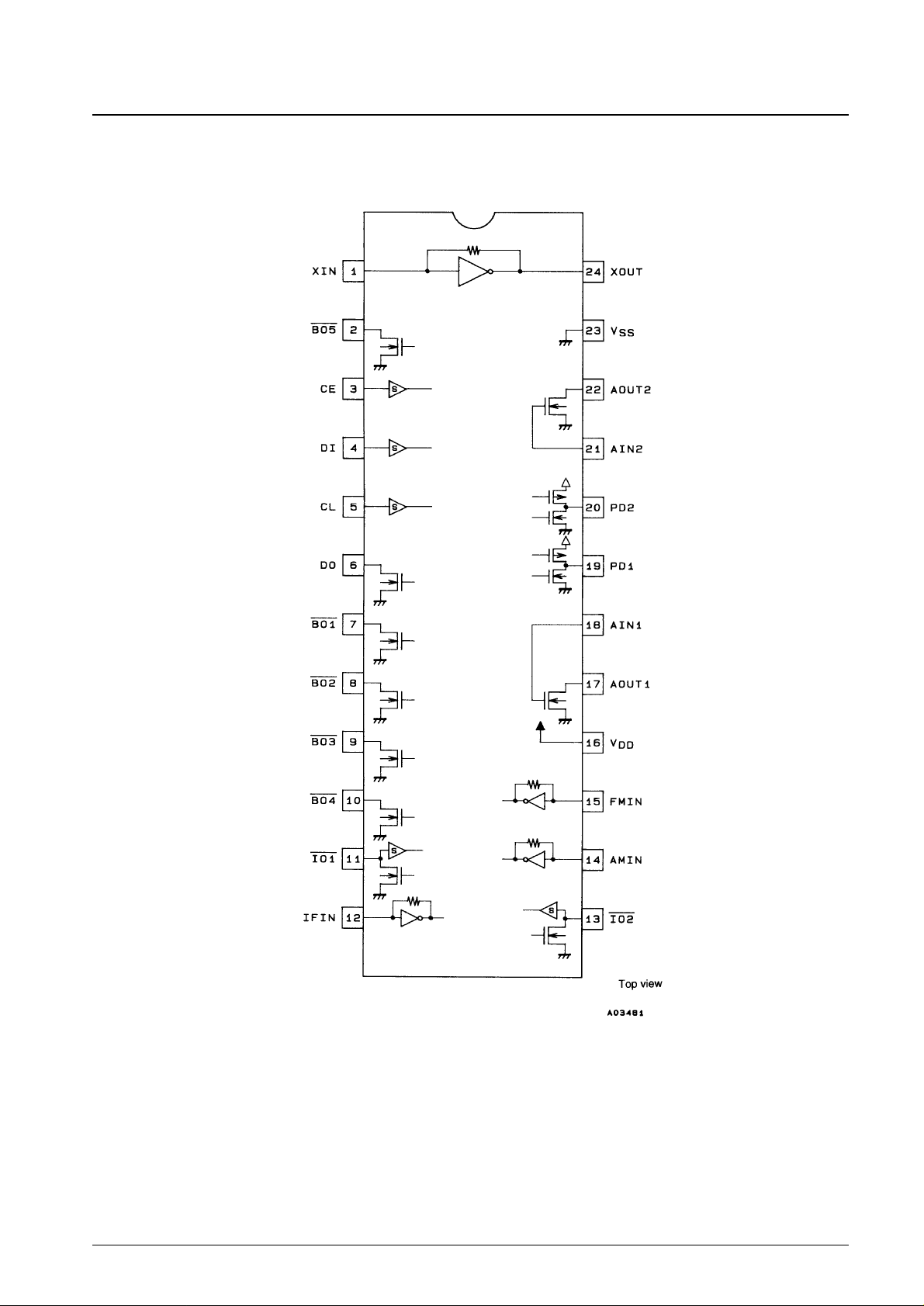
Pin Assignment
No. 4973-2/22
LC72130, 72130M

Block Diagram
No. 4973-3/22
LC72130, 72130M
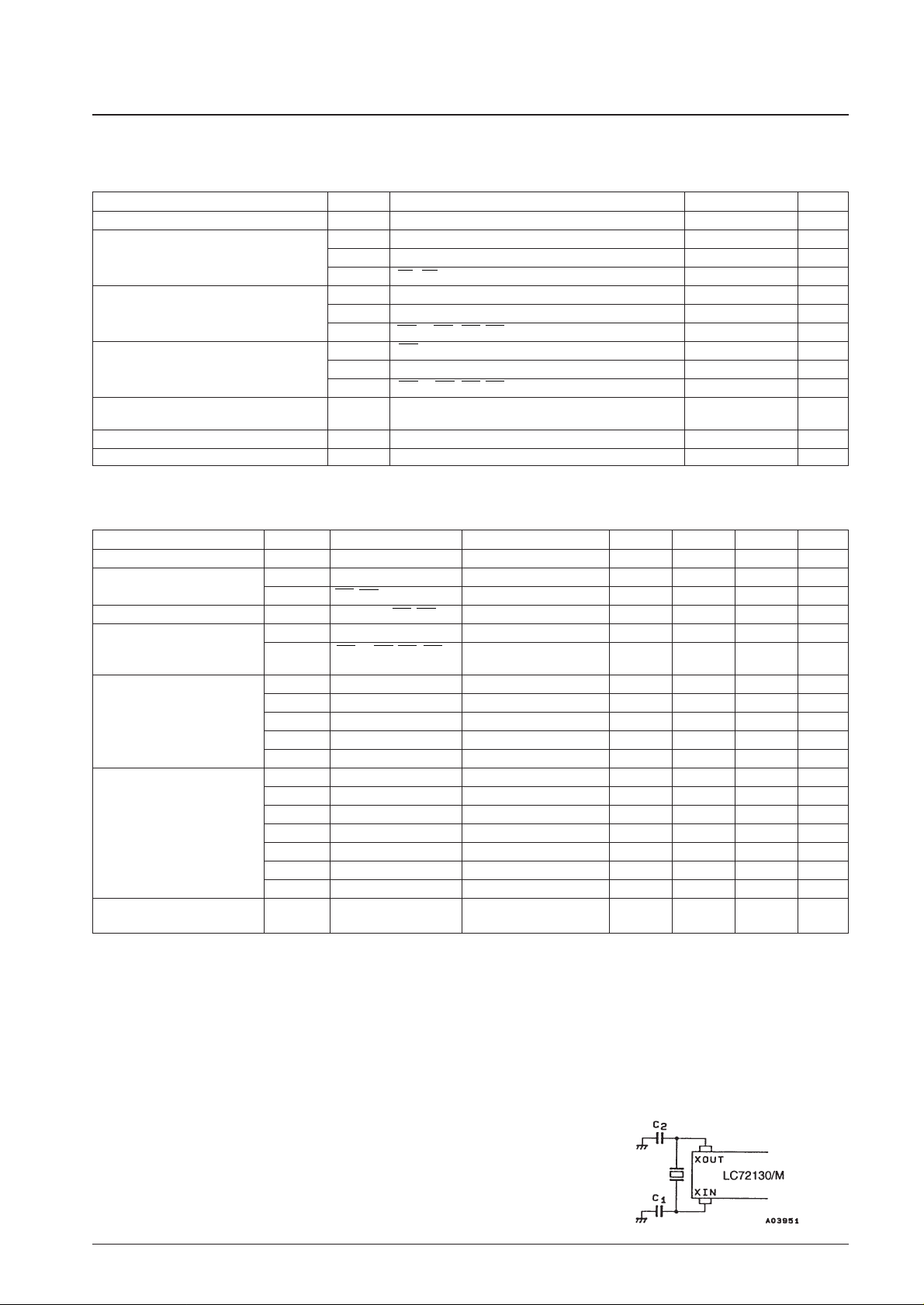
Specifications
Absolute Maximum Ratings at Ta = 25°C, VSS= 0 V
Allowable Operating Ranges at Ta = –40 to +85°C, VSS= 0 V
Note: * Recommended crystal oscillator CI values:
CI ≤ 120Ω (For a 4.5 MHz crystal)
CI ≤ 70Ω (For a 7.2 MHz crystal)
However, since the oscillator circuit characteristics depend on the printed circuit board and component values actually used, we recommend
requesting a circuit evaluation from the manufacturer of the crystal used.
<Sample Ocsillator Circuit>
Crystal oscillator: HC-49/U (manufactured by Kinseki, Ltd.), CL = 12 pF
C1 = C2 = 15 pF
The circuit constants for the crystal oscillator circuit depend on the crystal used, the printed circuit board pattern, and other items. Therefore we
recommend consulting with the manufacturer of the crystal for evaluation and reliability.
No. 4973-4/22
LC72130, 72130M
Parameter Symbol Pins Ratings Unit
Maximum supply voltage V
DD
max V
DD
–0.3 to +7.0 V
V
IN
1 max CE, CL, DI, AIN1, AIN2 –0.3 to +7.0 V
Maximum input voltage V
IN
2 max XIN, FMIN, AMIN, IFIN –0.3 to VDD+ 0.3 V
V
IN
3 max IO1, IO2 –0.3 to +15 V
V
O
1 max DO –0.3 to +7.0 V
Maximum output voltage V
O
2 max XOUT, PD1, PD2 –0.3 to VDD+ 0.3 V
V
O
3 max BO1 to BO5, IO1, IO2, AOUT1, AOUT2 –0.3 to +15 V
I
O
1 max BO1 0 to 3.0 mA
Maximum output current I
O
2 max DO, AOUT1, AOUT2 0 to 6.0 mA
I
O
3 max BO2 to BO5, IO1, IO2 0 to 10.0 mA
Allowable power dissipation Pd max Ta ≤ 85°C
DIP24S: 350
mW
MFP24S: 200
Operating temperature Topr –40 to +85 °C
Storage temperature Tstg –55 to +125 °C
Parameter Symbol Pins Conditions min typ max Unit
Supply voltage V
DD
V
DD
4.5 5.5 V
Input high level voltage
V
IH
1 CE, CL, DI 0.7 V
DD
6.5 V
V
IH
2 IO1, IO2 0.7 V
DD
13 V
Input low level voltage V
IL
CE, CL, DI, IO1, IO2 0 0.3 V
DD
V
V
O
1 DO 0 6.5 V
Output voltage
V
O
2
BO1 to BO5, IO1, IO2,
0 13 V
AOUT1, AOUT2
f
IN
1 XIN VIN1 1 8 MHz
f
IN
2 FMIN VIN2 10 160 MHz
Input frequency f
IN
3 AMIN VIN3, SNS = 1 2 40 MHz
f
IN
4 AMIN VIN4, SNS = 0 0.5 10 MHz
f
IN
5 IFIN VIN5 0.4 12 MHz
V
IN
1 XIN fIN1 400 1500 mVrms
V
IN
2-1 FMIN f = 10 to 130 MHz 40 1500 mVrms
V
IN
2-2 FMIN f = 130 to 160 MHz 70 1500 mVrms
Input amplitude V
IN
3 AMIN fIN3 , SNS = 1 40 1500 mVrms
V
IN
4 AMIN fIN4 , SNS = 0 40 1500 mVrms
V
IN
5 IFIN fIN5, IFS = 1 40 1500 mVrms
V
IN
6 IFIN fIN6, IFS = 0 70 1500 mVrms
Oscillation-guaranteed
crystal resonator
Xtal XIN, XOUT * 4.0 8.0 MHz

Electrical Characteristics at Ta = –40 to +85°C, VSS= 0 V
No. 4973-5/22
LC72130, 72130M
Parameter Symbol Pins Conditions min typ max Unit
Rf1 XIN 1.0 MΩ
Built-in feedback resistance
Rf2 FMIN 500 kΩ
Rf3 AMIN 500 kΩ
Rf4 IFIN 250 kΩ
Built-in pull-down resistor
Rpd1 FMIN 200 kΩ
Rpd2 AMIN 200 kΩ
Hysteresis V
HIS
CE, CL, DI, IO1, IO2 0.1 V
DD
V
Output high level voltage V
OH
1 PD1, PD2 IO = –1 mA VDD– 1.0 V
V
OL
1 PD1, PD2 IO = 1 mA 1.0 V
V
OL
2 BO1
IO = 0.5 mA 0.5 V
IO = 1 mA 1.0 V
V
OL
3 DO
IO = 1 mA 0.2 V
Output low level voltage IO = 5 mA 1.0 V
IO = 1 mA 0.2 V
V
OL
4 BO2 to BO5, IO1, IO2 IO = 5 mA 1.0 V
IO = 8 mA 1.6 V
V
OL
5 AOUT1, AOUT2 IO = 1 mA, AIN = 1.3 V 0.5 V
I
IH
1 CE, CL, DI VI= 6.5 V 5.0 V
I
IH
2 IO1, IO2 VI= 13 V 5.0 µA
Input high level current
I
IH
3 XIN VI= V
DD
2.0 11 µA
I
IH
4 FMIN, AMIN VI= V
DD
4.0 22 µA
I
IH
5 IFIN VI= V
DD
8.0 44 µA
I
IH
6 AIN1, AIN2 VI= 6.5 V 200 nA
I
IL
1 CE, CL, DI VI= 0 V 5.0 µA
I
IL
2 IO1, IO2 VI= 0 V 5.0 µA
Input low level current
I
IL
3 XIN VI= 0 V 2.0 11 µA
I
IL
4 FMIN, AMIN VI= 0 V 4.0 22 µA
I
IL
5 IFIN VI= 0 V 8.0 44 µA
I
IL
6 AIN1, AIN2 VI= 0 V 200 nA
I
OFF
1
BO1 to BO5, AOUT1,
VO= 13 V 5.0 µA
Output off leakage current
AOUT2, IO1, IO2
I
OFF
2 DO VO= 6.5 V 5.0 µA
High level three-state
I
OFFH
PD1, PD2, VO= V
DD
0.01 200 nA
off leakage current
Low level three-state
I
OFFL
PD1, PD2 VO= 0 V 0.01 200 nA
off leakage current
Input capacitance C
IN
FMIN 6 pF
Xtal = 7.2 MHz,
IDD1 V
DD
fIN2 = 130 MHz, 5 10 mA
V
IN
2-1= 40 mVrms
PLL block stopped
Current drain
I
DD
2 V
DD
(PLL INHIBIT),
0.5 mA
Xtal oscillator operating
(Xtal = 7.2 MHz)
IDD3 V
DD
PLL block stopped
10 µA
Xtal oscillator stopped

Pin Functions
No. 4973-6/22
LC72130, 72130M
Symbol Pin No. Type Functions Circuit configuration
XIN
XOUT
FMIN
AMIN
CE
CL
DI
DO
V
DD
1
24
15
14
3
5
4
6
16
X’tal OSC
Local oscillator
signal input
Local oscillator
signal input
Chip enable
Clock
Data input
Data output
Power supply
• Crystal resonator connection
(4.5/7.2 MHz)
• Serial data input: FMIN is selected when DVS is set to 1.
• The input frequency range is from 10 to 160 MHz.
• The signal is passed through a built-in divide-by-two
prescaler and then supplied to the swallow counter.
• Although the range of divisor settings is from 272 to
65,535, the actual divisor is twice the setting since there
is also a built-in divide-by-two prescaler.
• Serial data input: AMIN is selected when DVS is set to 0.
• Serial data input: When SNS is set to 1:
— The input frequency range is from 2 to 40 MHz.
— The signal is supplied directly to the swallow counter.
— The range of divisor settings is from 272 to 65,535
and the actual divisor will be the value set.
• Serial data input: When SNS is set to 0:
— The input frequency range is from 0.5 to 10 MHz.
— The signal is supplied directly to a 12-bit
programmable divider.
— The range of divisor settings is from 4 to 4,095 and
the actual divisor will be the value set.
• Must be set high when serial data is input to the
LC72130 (DI), or when serial data is output (DO).
• Used as the synchronization clock when serial data is
input to the LC72130 (DI), or when serial data is output
(DO).
• Inputs serial data sent from the controller to the
LC72130.
• Outputs serial data sent from the LC72130 to the
controller.
The content of the output data is determined by the
serial data DOC0 to DOC2.
• The LC72130 power supply (V
DD
= 4.5 to 5.5 V)
• The power on reset circuit operates when power is first
applied.
Continued on next page.
-
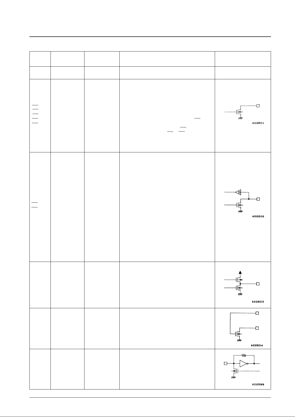
Continued from preceding page.
No. 4973-7/22
LC72130, 72130M
Symbol Pin No. Type Functions Circuit configuration
V
SS
BO1
BO2
BO3
BO4
BO5
IO1
IO2
PD1
PD2
AIN1
AOUT1
AIN2
AOUT2
IFIN
23
7
8
9
10
2
11
13
19
20
18
17
21
22
12
Ground
Output port
I/O port
Charge pump
output
LPF amplifier
transistor
IF counter
• The LC72130 ground —
• Dedicated output pins
• The output states are determined by BO1 to BO5 in the
serial data.
Data: 0 = open, 1 = low
• These pins go to the open state after the power on reset.
• An 8 Hz time base signal can be output from BO1 when
TBC in the serial data is set to 1.
• Note that the ON impedance of the BO1 pin is higher
than that of the other pins (BO2 to BO5).
• Pins used for both input and output
• The input or output state is determined by bits IOC1 and
IOC2 in the serial data.
Data: 0 = input port, 1 = output port
• When specified for use as an input port:
The input state is transmitted to the controller through
the DO pin.
Input state: Low
→ data value = 0
High → data value = 1
• When specified for use as an output port:
The output state is determined by bits IO1 and IO2 in the
serial data.
Data: 0 = open, 1 = low
• These pins go to the input port state after the power ON
reset.
• PLL charge pump output
When the frequency generated by dividing the local
oscillator frequency by N is higher than the reference
frequency, a high level will be output from the PD pin.
Similarly, when that frequency is lower, a low level will
be output. The PD pin goes to the high impedance state
when the frequencies agree.
• The MOS transistor used for the PLL active low-pass
filter.
• The input frequency range is from 0.4 to 12 MHz.
• The signal is supplied directly to the IF counter.
• The result from the IF counter MSB is output through the
DO pin.
• There are four measurement periods: 4, 8, 32, or 64 ms.
 Loading...