

SANYO LC66354C, LC66358C, LC66356C Datasheet

CMOS LSI
No. 5484
Four-Bit Single-Chip Microcontrollers
Preliminary
Overview
The LC66354C, LC66356C, and LC66358C are 4-bit
CMOS microcontrollers that integrate on a single chip all
the functions required in a system controller, including
ROM, RAM, I/O ports, a serial interface, comparator
inputs, three-value inputs, timers, and interrupt functions.
These three microcontrollers are available in a 42-pin
package.
These products differ from the earlier LC66358A Series
and LC66358B Series in the power-supply voltage range,
the operating speed, and other points.
Features and Functions
• On-chip ROM capacities of 4, 6, and 8 kilobytes, and an
on-chip RAM capacity of 512 × 4 bits.
• Fully supports the LC66000 Series common instruction
set (128 instructions).
• I/O ports: 36 pins
• 8-bit serial interface: two circuits (can be connected in
cascade to form a 16-bit interface)
• Instruction cycle time: 0.92 to 10 µs (at 2.5 to 5.5 V)
— For the earlier LC66358A Series: 1.96 to 10 µs (at
3.0 to 5.5 V) and 3.92 to 10 µs (at 2.2 to 5.5 V)
— For the earlier LC66358B Series: 0.92 to 10 µs (at
3.0 to 5.5 V)
• Powerful timer functions and prescalers
— Time limit timer, event counter, pulse width
measurement, and square wave output using a 12-bit
timer.
— Time limit timer, event counter, PWM output, and
square wave output using an 8-bit timer.
— Time base function using a 12-bit prescaler.
• Powerful interrupt system with 8 interrupt factors and 8
interrupt vector locations.
— External interrupts: 3 factors/3 vector locations
— Internal interrupts: 5 factors/5 vector locations
• Flexible I/O functions
Comparator inputs, three-value inputs, 20-mA drive
outputs, 15-V high-voltage pins, and pull-up/open-drain
options.
• Optional runaway detection function (watchdog timer)
• 8-bit I/O functions
• Power saving functions using halt and hold modes.
• Packages: DIP42S, QIP48E (QFP48E)
LC66354C, 66356C, 66358C
with 4, 6, and 8 KB of On-Chip ROM
• Evaluation LSIs
— LC66599 (evaluation chip) + EVA85/800-TB6630X
— LC66E308 (on-chip EPROM microcontroller)
used together.
Package Dimensions
unit: mm
3025B-DIP42S
[LC66354C/66356C/66358C]
1.78
22
21
4.25
0.51
min
1.15
SANYO: DIP42S
1.6
1.5
25
24
13
SANYO: QFP48E
13.8
15.24
5.1
max
3.8
0.15
0.1
2.70
(STAND OFF)
42
1
unit: mm
3156-QFP48E
1.614.0
17.2
3.0max
37.9
0.95 0.48
[LC66354C/66356C/66358C]
17.2
14.0
1.0
1.5
36
37
1.5
1.0
1.5
48
112
0.35
0.8
15.6
0.25
SANYO Electric Co.,Ltd. Semiconductor Bussiness Headquarters
TOKYO OFFICE Tokyo Bldg., 1-10, 1 Chome, Ueno, Taito-ku, TOKYO, 110 JAPAN
22897HA (OT) No. 5484-1/21
Series Organization
LC66354C, 66356C, 66358C
Type No.
LC66304A/306A/308A 42 4 K/6 K/8 KB 512 W DIP42S QFP48E
LC66404A/406A/408A 42 4 K/6 K/8 KB 512 W DIP42S QFP48E
LC66506B/508B/512B/516B 64 6 K/8 K/12 K/16 KB 512 W DIP64S QFP64A
LC66354A/356A/358A 42 4 K/6 K/8 KB 512 W DIP42S QFP48E
LC66354S/356S/358S 42 4 K/6 K/8 KB 512 W QFP44M
LC66556A/558A/562A/566A 64 6 K/8 K/12 K/16 KB 512 W DIP64S QFP64E
LC66354B/356B/358B 42 4 K/6 K/8 KB 512 W DIP42S QFP48E
LC66556B/558B 64 6 K/8 KB 512 W DIP64S QFP64E
LC66562B/566B 64 12 K/16 KB 512 W DIP64S QFP64E
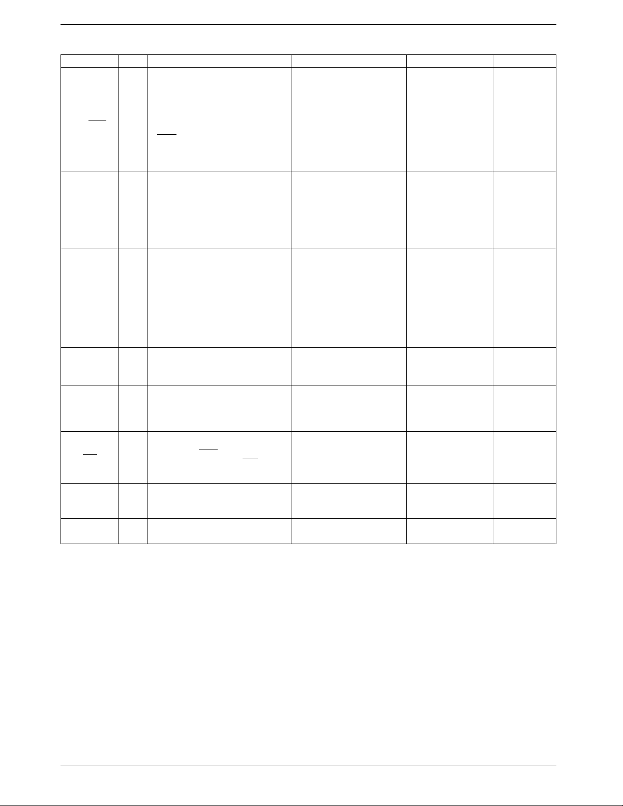
LC66354C/356C/358C 42 4 K/6 K/8 KB 512 W DIP42S QFP48E 2.5 to 5.5 V/0.92 µs
LC662304A/2306A/2308A 42 4 K/6 K/8 KB 512 W DIP42S QFP48E
LC662312A/2316A 42 12 K/16 KB 512 W DIP42S QFP48E
LC665304A/665306A/665308A 48 4 K/6 K/8 KB 512 W DIP48S QFP48E
LC665312A/5316A 48 12 K/16 KB 512 W DIP48S QFP48E
LC66E308 42 EPROM 8 KB 512 W
LC66P308 42 OTPROM 8 KB 512 W DIP42S QFP48E
LC66E408 42 EPROM 8 KB 512 W
LC66P408 42 OTPROM 8 KB 512 W DIP42S QFP48E
LC66E516 64 EPROM 16 KB 512 W
LC66P516 64 OTPROM 16 KB 512 W DIP64S QFP64E
LC66E2316 42 EPROM 16 KB 512 W
LC66E5316 52/48 EPROM 16 KB 512 W
LC66P2316* 42 OTPROM 16 KB 512 W DIP42S QFP48E
LC66P5316 48 OTPROM 16 KB 512 W DIP48S QFP48E
Note: * Under development
No. of
pins capacity
ROM capacity
RAM
DIC42S QFC48
with window with window
DIC42S QFC48
with window with window
DIC64S QFC64
with window with window
DIC42S QFC48
with window with window
DIC52S QFC48
with window with window
Package Features
Normal versions
4.0 to 6.0 V/0.92 µs
Low-voltage versions
2.2 to 5.5 V/3.92 µs
Low-voltage high-speed versions
3.0 to 5.5 V/0.92 µs
On-chip DTMF generator versions
3.0 to 5.5 V/0.95 µs
Dual oscillator support
3.0 to 5.5 V/0.95 µs
Window and OTP evaluation versions
4.5 to 5.5 V/0.92 µs
4.5 to 5.5 V/0.95 µs
4.0 to 5.5 V/0.95 µs
No. 5484-2/21
Pin Assignments
LC66354C, 66356C, 66358C
DIP42S
P00
P01
P02
P03
P10
P11
P12
P13
SI0/P20
SO0/P21
SCK0/P22
INT0/P23
INT1/P30
POUT0/P31
POUT1/P32
HOLD/P33
P40
P41
TEST
V
SS
OSC1
10
11
12
13
14
15
16
17
18
19
20
21
1
2
3
4
5
6
7
8
9
LC66354C
356C
358C
PE1/TRB
42
PE0/TRA
41
V
40
PD3/CMP3
39
PD2/CMP2
38
PD1/CMP1
37
PD0/CMP0
36
PC3/VREF1
35
PC2/VREF0
34
P63/PIN1
33
P62/SCK1
32
P61/SO1
31
P60/SI1
30
P53/INT2
29
P52
28
P51
27
P50
26
P43
25
P42
24
RES
23
OSC2
22
DD
QFP48E
PD1/CMP1
PD0/CMP0
PC3/VREF1
PC2/VREF0
P63/PIN1
P62/SCK1
NC
P61/S01
P60/S11
P53/INT2
P52
P51
36
35
34
33
32
31
30
29
28
27
26
25
37CMP2/PD2
38CMP3/PD3
39V
DD
40TRA/PE0
41TRB/PE1
42NC 19 NC
43NC 18 NC
44P00
45P01 16 V
46P02
47P03 14 P41
48P10
1
2
P11
P12
3
4
P13
LC66354C
356C
358C
5
6
NC
S10/P20
S00/P21
7
8
9
INT0/P23
SCK0/P22
10
INT1/P30
24 P50
23 P43
22 P42
21 RES
20 OSC2
17 OSC1
15 TEST
13 P40
11
12
HOLD/P33
POUT0/P31
POUT1/P32
SS
Top view
We recommend the use of reflow-soldering techniques to solder-mount QFP packages.
Please consult with your Sanyo representative for details on process conditions if the package itself is to be directly
immersed in a dip-soldering bath (dip-soldering techniques).
No. 5484-3/21
System Block Diagram
LC66354C, 66356C, 66358C
RES
TEST
OSC1
OSC2
HOLD
TRA
TRB
CMP0
CMP1
CMP2
CMP3
SYSTEM
CONTROL
PE
PD
PC
RAM STACK
(512W)
FLAG
D
D
D
E
SP E A
M
R
D
P
P
P
P
L
H
X
Y
PRESCALER
CZ
MPX TIMER0 SERIAL I/O 0
MPX
INTERRUPT
CONTROL
MPX
ALU
TIMER1
SERIAL I/O 1
ROM
(4K/6K/8K)
PC
POUT0
SI0
SO0
SCK0
INT0
INT1. INT2
SI1
SO1
SCK1
PIN1. POUT1
P0 P1 P2 P3 P4 P5 P6
Differences between the LC66354C, LC66356C, and LC66358C and the LC6630X Series
Item
System differences
Hardware wait time (number of cycles)
when hold mode is cleared
Value of timer 0 after a reset
(Including the value after hold mode is Set to FF0. Set to FFC.
cleared)
Difference in major features
Operating power-supply voltage and
operating speed (cycle time)
Note: 1. An RC oscillator cannot be used with the LC66354C, LC66356C, and LC66358C.
2. There are other differences, including differences in output currents and port input voltages.
For details, see the data sheets for the LC66308A, LC66E308, and LC66P308.
3. Pay close attention to the differences listed here when using the LC66E308 and LC66P308 for evaluation.
(Including the LC66599 evaluation chip)
65536 cycles 16384 cycles
About 64 ms at 4 MHz (Tcyc = 1 µs) About 16 ms at 4 MHz (Tcyc = 1 µs)
• LC66304A/306A/308A • LC6635XA
4.0 to 6.0 V/0.92 to 10 µs 2.2 to 5.5 V/3.92 to 10 µs
• LC66E308/P308 3.0 to 5.5 V/1.96 to 10 µs
4.5 to 5.5 V/0.92 to 10 µs • LC6635XB
LC6630X Series
2.5 to 5.5 V/0.92 to 10 µs
3.0 to 5.5 V/0.92 to 10 µs
LC6635XC Series
No. 5484-4/21
LC66354C, 66356C, 66358C
Pin Function Overview
Pin I/O Overview Output driver type Options State after a reset
P00
P01
P02
P03
P10
P11
P12
P13
P20/SI0
P21/SO0
P22/SCK0
P23/INT0
P30/INT1
P31/POUT0
P32/POUT1
I/O ports P00 to P03
• Input or output in 4-bit or 1-bit units
I/O
• P00 to P03 support the halt mode control
function
I/O ports P10 to P13
I/O
Input or output in 4-bit or 1-bit units
I/O ports P20 to P23
• Input or output in 4-bit or 1-bit units
• P20 is also used as the serial input SI0
pin.
• P21 is also used as the serial output
SO0 pin.
I/O
• P22 is also used as the serial clock
SCK0 pin.
• P23 is also used as the INT0 interrupt
request pin, and also as the timer 0
event counting and pulse width
measurement input.
I/O ports P30 to P32
• Input or output in 3-bit or 1-bit units
• P30 is also used as the INT1 interrupt
request.
I/O
• P31 is also used for the square wave
output from timer 0.
• P32 is also used for the square wave
output from timer 1.
• Pch: Pull-up MOS type
• Nch: Intermediate sink current
type
• Pch: Pull-up MOS type
• Nch: Intermediate sink current
type
• Pch: CMOS type
• Nch: Intermediate sink current
type
• Nch: +15-V handling when OD
option selected
• Pch: CMOS type
• Nch: Intermediate sink current
type
• Nch: +15-V handling when OD
option selected
• Pull-up MOS or Nch
OD output
• Output level on reset
• Pull-up MOS or Nch
OD output
• Output level on reset
CMOS or Nch OD
output
CMOS or Nch OD
output
High or low
(option)
High or low
(option)
H
H
P33/HOLD
P40
P41
P42
P43
P50
P51
P52
P53/INT2
Hold mode control input
• Hold mode is set up by the HOLD
instruction when HOLD is low.
• In hold mode, the CPU is restarted by
setting HOLD to the high level.
• This pin can be used as input port P33
I
along with P30 to P32.
• When the P33/HOLD pin is at the low
level, the CPU will not be reset by a low
level on the RES pin. Therefore,
applications must not set P33/HOLD low
when power is first applied.
I/O ports P40 to P43
• Input or output in 4-bit or 1-bit units
• Input or output in 8-bit units when used
in conjunction with P50 to P53.
I/O
• Can be used for output of 8-bit ROM
data when used in conjunction with P50
to P53.
I/O ports P50 to P53
• Input or output in 4-bit or 1-bit units
• Input or output in 8-bit units when used
in conjunction with P40 to P43.
• Can be used for output of 8-bit ROM
I/O
data when used in conjunction with P40
to P43.
• P53 is also used as the INT2 interrupt
request.
• Pch: Pull-up MOS type
• Nch: Intermediate sink current
type
• Nch: +15-V handling when OD
option selected
• Pch: Pull-up MOS type
• Nch: Intermediate sink current
type
• Nch: +15-V handling when OD
option selected
Pull-up MOS or Nch OD
output
Pull-up MOS or Nch OD
output
H
H
Continued on next page.
No. 5484-5/21
LC66354C, 66356C, 66358C
Continued from preceding page.
Pin I/O Overview Output driver type Options State after a reset
I/O ports P60 to P63
• Input or output in 4-bit or 1-bit units
P60/SI0
P61/SO1
P62/SCK1
P63/PIN1
PC2/VREF0
PC3/VREF1
PD0/CMP0
PD1/CMP1
PD2/CMP2
PD3/CMP3
• P60 is also used as the serial input SI1
pin.
• P61 is also used as the serial output
I/O
SO1 pin.
• P62 is also used as the serial clock
SCK1 pin.
• P63 is also used for the event count
input to timer 1.
I/O ports PC2 and PC3
• Input or output in 2-bit or 1-bit units
• PC2 is also used as the VREF0
I/O
comparator comparison voltage pin.
• PC3 is also used as the VREF1
comparator comparison voltage pin.
Dedicated input ports PD0 to PD3
• These pins can be switched in software
to function as comparator inputs.
• The comparison voltage for PD0 is
provided by VREF0.
I
• The comparison voltage for PD1 to PD3
is provided by VREF1.
• Pins PD0 and PD1 can be set to the
comparator function individually, but pins
PD2 and PD3 are set together.
• Pch: CMOS type
• Nch: Intermediate sink current
type
• Nch: +15-V handling when OD
option selected
• Pch: CMOS type
• Nch: Intermediate sink current
type
CMOS or Nch OD
output
CMOS or Nch OD
output
Normal input
H
H
PE0/TRA
PE1/TRB
OSC1
OSC2
Dedicated input ports
I
These pins can be switched in software to
function as three-value inputs.
System clock oscillator connections
I
When an external clock is used, leave
OSC2 open and connect the clock signal
O
to OSC1.
System reset input
When the P33/HOLD pin is at the high
RES
I
level, a low level input to the RES pin will
initialize the CPU.
CPU test pin
TEST
V
DD
V
SS
I
This pin must be connected to V
normal operation.
Power supply pins
SS
during
Note: Pull-up MOS type: The output circuit includes a MOS transistor that pulls the pin up to V
CMOS output: Complementary output.
OD output: Open-drain output.
DD
Normal input
Use of either a ceramic
oscillator or an external
clock can be selected.
.
No. 5484-6/21
LC66354C, 66356C, 66358C
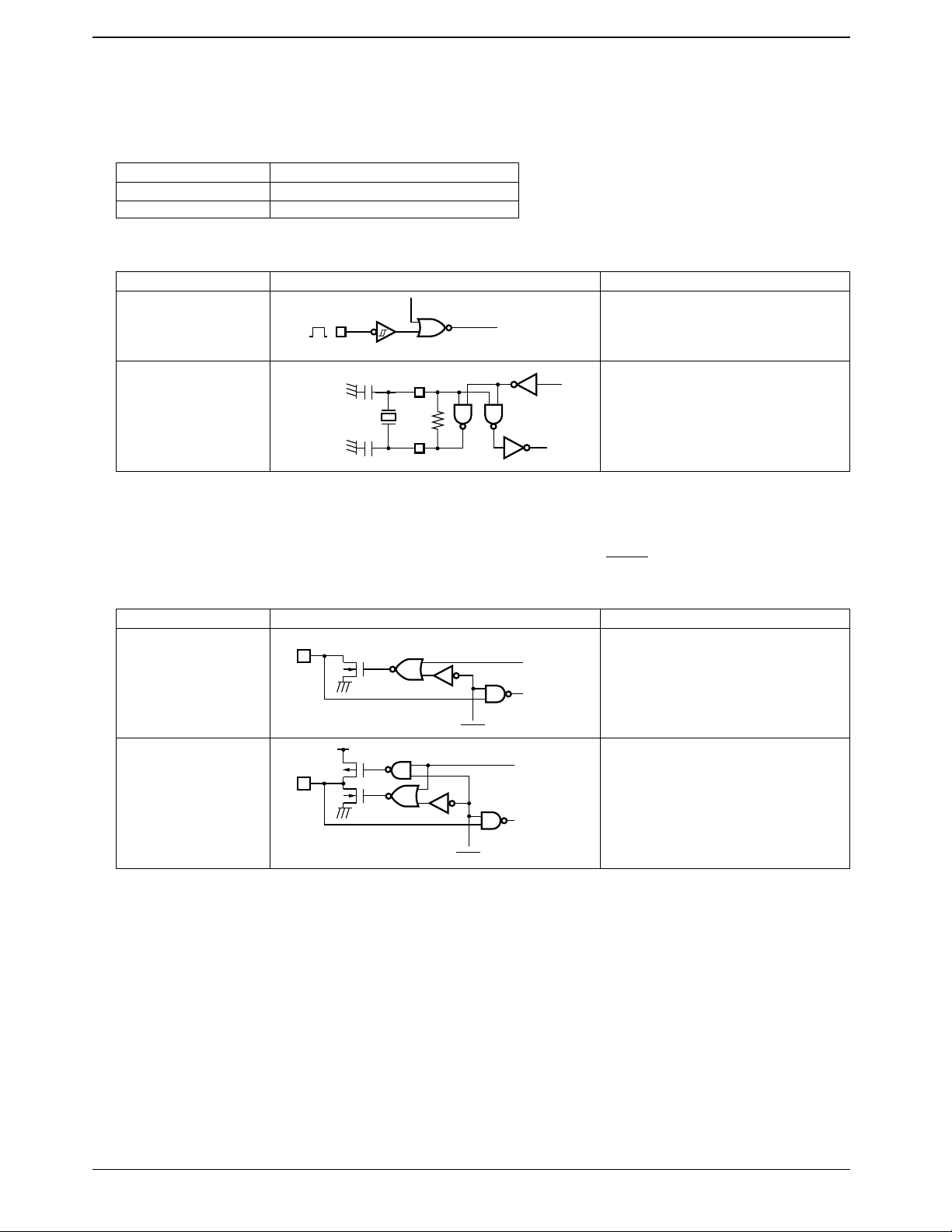
User Options
1. Port 0 and 1 output level at reset option
The output levels at reset for I/O ports 0 and 1, in independent 4-bit groups, can be selected from the following two
options.
Option Conditions and notes
1. Output high at reset The four bits of ports 0 or 1 are set in a group
2. Output low at reset The four bits of ports 0 or 1 are set in a group
2. Oscillator circuit options
Option Circuit Conditions and notes
1. External clock
2. Ceramic oscillator
Note: There is no RC oscillator option.
OSC1
C1
Ceramic oscillator
C2
The input has Schmitt characteristics
OSC1
OSC2
3. Watchdog timer option
A runaway detection function (watchdog timer) can be selected as an option.
4. Port output type options
• The output type of each bit (pin) in ports P0, P1, P2, P3 (except for the P33/HOLD pin), P4, P5, P6, and PC can be
selected individually from the following two options.
Option Circuit Conditions and notes
1. Open-drain output
2. Output with built-in pull-up
resistor
Output data
Input data
DSB
Output data
Input data
DSB
The port P2, P3, P5, and P6 inputs have Schmitt
characteristics.
The port P2, P3, P5, and P6 inputs have Schmitt
characteristics.
The CMOS outputs (ports P2, P3, P6, and PC)
and the pull-up MOS outputs (P0, P1, P4, and
P5) are distinguished by the drive capacity of the
p-channel transistor.
• The port PD comparator input and the port PE three-value input are selected in software.
No. 5484-7/21
 Loading...