

SANYO LC322271T-80, LC322271T-70, LC322271M-80, LC322271M-70, LC322271J-80 Datasheet
...
Ordering number : EN*5085A
32896HA (OT)/33195TH (OT) No. 5085-1/29
Overview
The LC322271J, M and T is a CMOS dynamic RAM
operating on a single 5 V power source and having a
131072 words × 16 bits configuration. Equipped with
large capacity capabilities, high speed transfer rates and
low power dissipation, this series is suited for a wide
variety of applications ranging from computer main
memory and expansion memory to commercial
equipment.
Address input utilizes a multiplexed address bus which
permits it to be enclosed in a compact plastic package of
SOJ 40-pin, SOP 40-pin, and TSOP 44-pin . Refresh rates
are within 8 ms with 512 row address (A0 to A7, A8R)
selection and support Row Address Strobe (RAS)-only
refresh, Column Address Strobe (CAS)-before-RAS
refresh and hidden refresh settings. There are functions
such as fast page mode, read-modify-write and byte write.
The pin assignment follows the JEDEC 1 M DRAM
(65536 words × 16 bits, 1CAS/2WE) standard.
Features
• 131072 words × 16 bits configuration.
• Single 5 V ± 10% power supply.
• All input and output (I/O) TTL compatible.
• Supports fast page mode, read-modify-write and byte
write.
• Supports output buffer control using early write and
Output Enable (OE) control.
• 8 ms refresh using 512 refresh cycles.
• Supports RAS-only refresh, CAS-before-RAS refresh
and hidden refresh.
• Follows the JEDEC 1 M DRAM (65536 words × 16
bits, 1CAS/2WE) standard.
• RAS access time/column address time/CAS access
time/cycle time/power dissipation
• Package:
SOJ 40-pin (400 mil) plastic package : LC322271J
SOP 40-pin (450 mil) plastic package: LC322271M
TSOP 44-pin (400 mil) plastic package : LC322271T
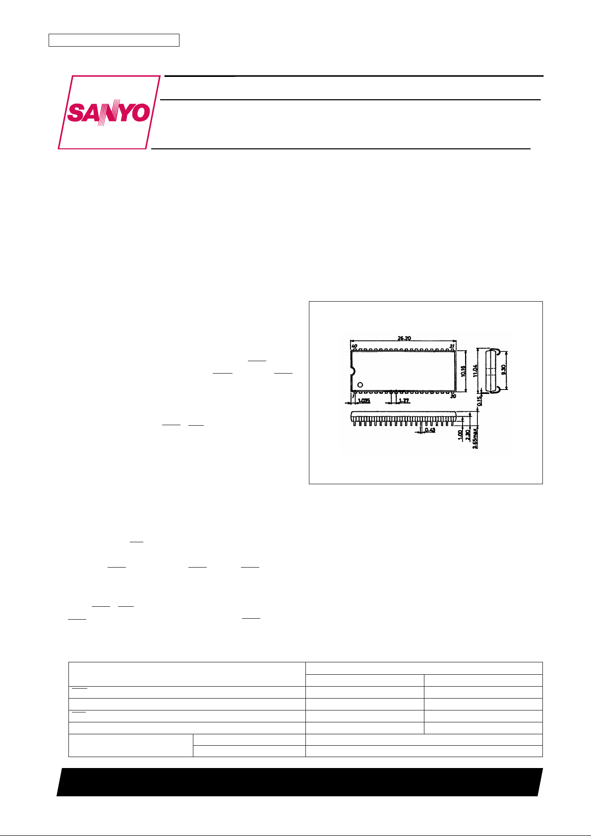
Package Dimensions
unit: mm
3200-SOJ40
Preliminary
SANYO: SOJ40
[LC322271J]
LC322271J, M, T-70/80
SANYO Electric Co.,Ltd. Semiconductor Bussiness Headquarters
TOKYO OFFICE Tokyo Bldg., 1-10, 1 Chome, Ueno, Taito-ku, TOKYO, 110-0005 JAPAN
2 MEG (131072 words × 16 bits) DRAM
Fast Page Mode, Byte Write
CMOS LSI
Parameter
LC322271J, M, T
-70 -80
RAS access time 70 ns 80 ns
Column address access time 35 ns 45 ns
CAS access time 20 ns 30 ns
Cycle time 130 ns 150 ns
Power dissipation (max.)
During operation 688 mW 633 mW
During standby 5.5 mW (CMOS level)/11 mW (TTL level)
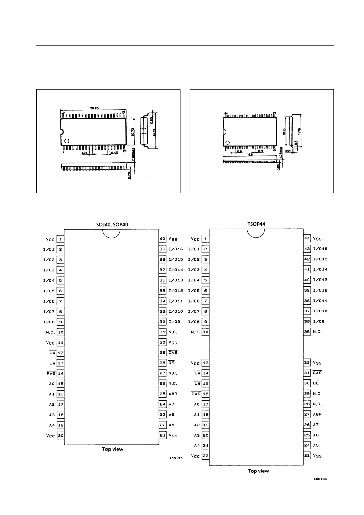
Package Dimensions
unit: mm
3195-SOP40
Pin Assignments
No. 5085-2/29
LC322271J, M, T-70/80
SANYO: SOP40
[LC322271M]
unit: mm
3207-TSOP44
SANYO: TSOP44 (TYPE II)
[LC322271T]

Block Diagram
Specifications
Absolute Maximum Ratings
Note: 1. Stresses greater than the above listed maximum values may result in damage to the device.
No. 5085-3/29
LC322271J, M, T-70/80
Parameter Symbol Ratings Unit Note
Maximum supply voltage V
CC
max –1.0 to +7.0 V 1
Input voltage V
IN
–1.0 to +7.0 V 1
Output voltage V
OUT
–1.0 to +7.0 V 1
Allowable power dissipation
LC322271J, M
Pd max
800
mW 1
LC322271T 700
Output short-circuit current I
OUT
50 mA 1
Operating temperature range Topr 0 to +70 °C 1
Storage temperature range Tstg –55 to +150 °C 1
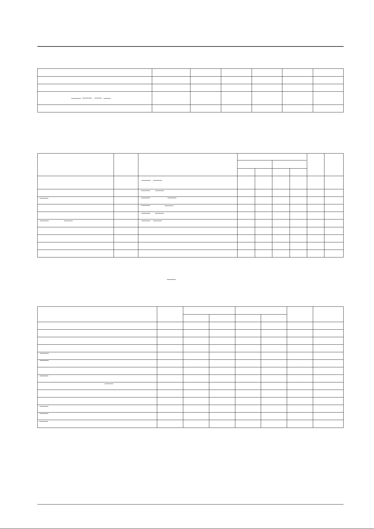
DC Recommended Operating Ranges at Ta = 0 to +70°C
Note: 2. All voltages are referenced to VSS.
*: –2.0 V when pulse width is less than 20 ns.
DC Electrical Characteristics at Ta = 0 to +70°C, VCC= 5 V ± 10%
Note: 3. All current values are measured at minimum cycle rate. Since current flows immoderately, if cycle time is longer than shown here, current value
becomes smaller.
4. I
CC1
and I
CC4
are dependent on output loads. Maximum values for I
CC1
and I
CC4
represent values with output open.
5. Address change is less than or equal to one time during RAS = V
IL
. Concerning I
CC4
, it is less than or equal to one time during 1 cycle (tPC).
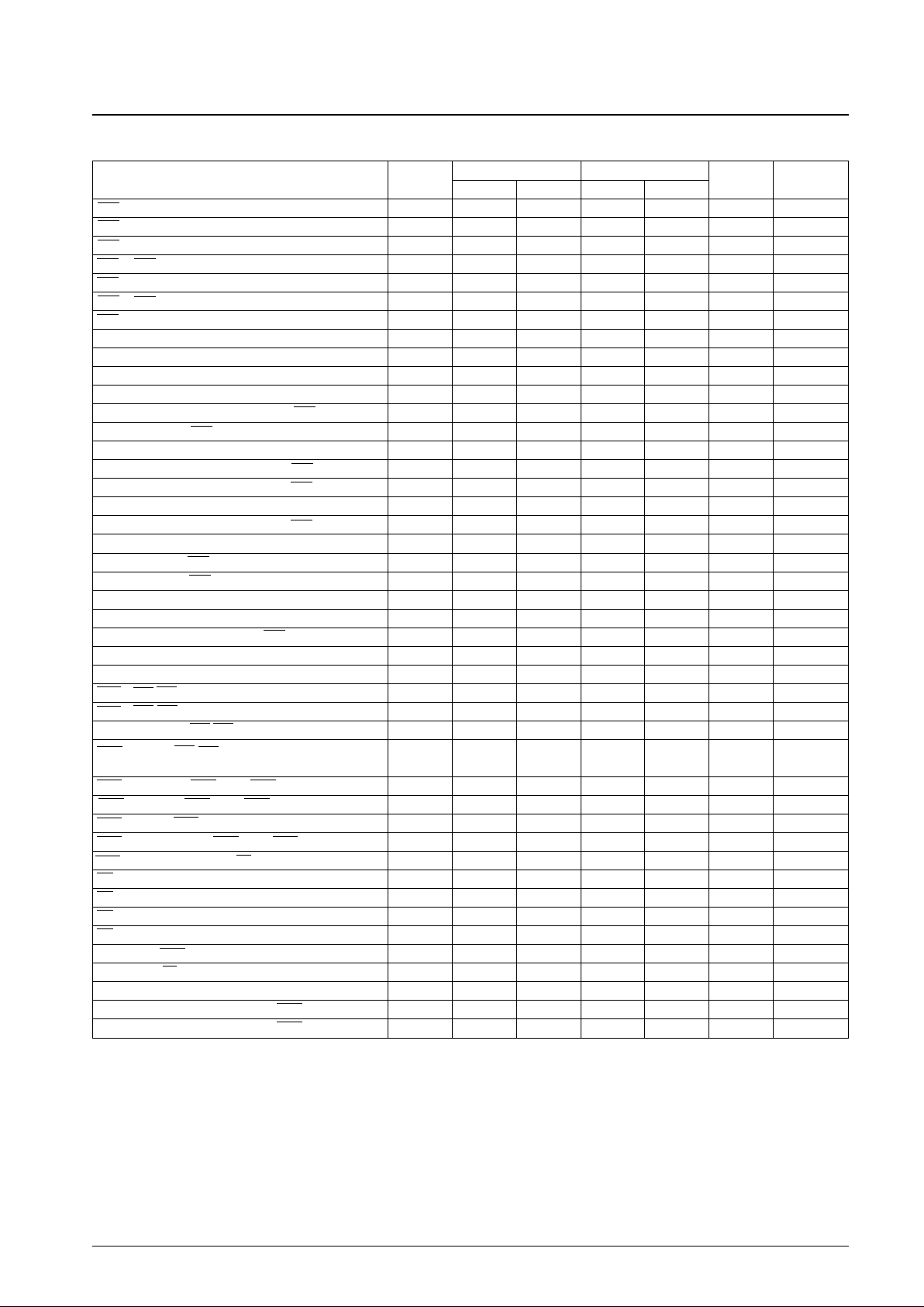
AC Electrical Characteristics at Ta = 0 to +70°C, VCC= 5 V ± 10% (Notes 6, 7 and 8)
No. 5085-4/29
LC322271J, M, T-70/80
Parameter Symbol min typ max Unit Note
Power supply voltage V
CC
4.5 5.0 5.5 V 2
Input high level voltage V
IH
2.4 6.5 V 2
Input low level voltage
V
IL
–1.0
*
+0.8 V 2
(A0 to A7, A8R, RAS, CAS, UW, LW, OE)
Input low level voltage (I/O1 to I/O16) V
IL
–0.5
*
+0.8 V 2
Parameter Symbol
-70 -80
Unit Note
min max min max
Random read, write cycle time t
RC
130 150 ns
Read-write/read-modify-write cycle time t
RWC
190 200 ns
Fast page mode cycle time t
PC
45 55 ns
Fast page mode read-write/read-modify-write cycle time t
PRWC
95 100 ns
RAS access time t
RAC
70 80 ns 9, 14, 15
CAS access time t
CAC
20 30 ns 9, 14
Column address access time t
AA
35 45 ns 9, 15
CAS precharge access time t
CPA
40 50 ns 9
Output low-impedance time from CAS low t
CLZ
0 0 ns 9
Output buffer turn-off delay time t
OFF
0 20 0 20 ns 10
Rise, fall time t
T
3 50 3 50 ns
RAS precharge time t
RP
50 60 ns
RAS pulse width t
RAS
70 10000 80 10000 ns
RAS pulse width for fast page mode cycle only t
RASP
70 100000 80 100000 ns
Continued on next page.
LC322271J, M, T
Parameter Symbol Conditions -70 -80 Unit Note
min max min max
Operating current
I
CC1
RAS, CAS, address cycling: tRC= tRCmin 125 115 mA 3, 4, 5
(Average current during operation)
Standby current I
CC2
RAS = CAS = V
IH
2 2 mA
RAS-only refresh current I
CC3
RAS cycling, CAS = VIH: tRC= tRCmin 125 115 mA 3, 5
Fast page mode current I
CC4
RAS = VIL, CAS, address cycling: tPC= tPCmin 115 90 mA 3, 4, 5
Standby current I
CC5
RAS = CAS = VCC– 0.2 V 1 1 mA
CAS-before-RAS refresh current I
CC6
RAS, CAS cycling: tRC= tRCmin 125 115 mA 3
Input leakage current I
IL
0 V ≤ VIN≤ 6.5 V, pins other than test pin = 0 V –10 +10 –10 +10 µA
Output leakage current I
OL
D
OUT
disable, 0 V ≤ V
OUT
≤ 5.5 V –10 +10 –10 +10 µA
Output high level voltage V
OHIOUT
= –2.5 mA 2.4 2.4 V
Output low level voltage V
OLIOUT
= 2.1 mA 0.4 0.4 V
Continued from preceding page.
No. 5085-5/29
LC322271J, M, T-70/80
-70 -80
Parameter
Symbol min max min max
Unit Note
RAS hold time t
RSH
20 30 ns
CAS hold time t
CSH
70 80 ns
CAS pulse width t
CAS
20 10000 30 10000 ns
RAS to CAS delay time t
RCD
25 50 25 50 ns 14
RAS to column address delay time t
RAD
17 35 17 35 ns 15
CAS to RAS precharge time t
CRP
10 10 ns
CAS precharge time t
CP
10 10 ns
Row address setup time t
ASR
0 0 ns
Row address hold time t
RAH
12 12 ns
Column address setup time t
ASC
0 0 ns
Column address hold time t
CAH
15 20 ns
Column address hold time referenced to RAS t
AR
50 60 ns
Column address to RAS lead time t
RAL
40 45 ns
Read command setup time t
RCS
0 0 ns
Read command hold time referenced to CAS t
RCH
0 0 ns 11
Read command hold time referenced to RAS t
RRH
0 0 ns 11
Write command hold time t
WCH
15 15 ns
Write command hold time referenced to RAS t
WCR
50 60 ns
Write command pulse width t
WP
15 15 ns
Write command to RAS lead time t
RWL
25 25 ns
Write command to CAS lead time t
CWL
20 20 ns
Data input setup time t
DS
0 0 ns 12
Data input hold time t
DH
15 20 ns 12
Data input hold time referenced to RAS t
DHR
50 60 ns
Refresh time t
REF
8 8 ms
Write command setup time t
WCS
0 0 ns 13
CAS to UW, LW delay time t
CWD
50 50 ns 13
RAS to UW, LW delay time t
RWD
100 100 ns 13
Column address to UW, LW delay time t
AWD
65 65 ns 13
CAS precharge UW, LW delay time for fast page mode
t
CPWD
70 70 ns 13
cycle only
CAS setup time for CAS-before-RAS t
CSR
10 10 ns
CAS hold time for CAS-before-RAS t
CHR
15 15 ns
RAS precharge CAS active time t
RPC
10 10 ns
CAS precharge time for CAS-before-RAS counter test t
CPT
40 40 ns
RAS hold time referenced to OE t
ROH
15 15 ns
OE access time t
OEA
20 25 ns 9
OE delay time t
OED
15 15 ns
OE output buffer turn-off delay time t
OEZ
0 0 15 ns 10
OE command hold time t
OEH
20 20 ns
Data input to CAS delay time t
DZC
0 0 ns 16
Data input to OE delay time t
DZO
0 0 ns 16
Masked write setup time t
MCS
0 0 ns
Masked write hold time referenced to RAS t
MRH
0 0 ns
Masked write hold time referenced to CAS t
MCH
0 0 ns

Input/Output Capacitance at Ta = 25°C, f = 1 MHz, VCC= 5 V ± 10%
Note: 6. An initial pause of 200 µs is required after power-up followed by eight RAS-only refresh cycles before proper device operation is achieved. In case
of using refresh counter, a minimum of eight CAS-before-RAS refresh cycles instead of eight RAS-only refresh cycles are required.
7. Measured at t
T
= 5 ns.
8. When measuring input signal timing, V
IH
(min) and VIL(max) are used for reference points. In addition, rise and fall time are defined between V
IH
and VIL.
9. Measured using an equivalent of 50 pF and one standard TTL loads.
10. t
OFF
(max) and t
OEZ
(max) are defined as the time until output voltage can no longer be measured when output switches to a high impedance
condition.
11. Operation is guaranteed if either t
RRH
or t
RCH
is satisfied.
12. These parameters are measured from the falling edge of CAS for an early-write cycle, and from the falling edge of UW and LW for a readwrite/read-modify-write cycle.
13. t
WCS
, t
CWD
, t
RWD
, t
AWD
and t
CPWD
are not restrictive operating parameters for memory in that they specify the operating mode. If t
WCS
≥ t
WCS
(min), the cycle switches to an early-write cycle and output pins switch to high impedance throughout the cycle.
If t
CWD
≥ t
CWD
(min), t
RWD
≥ t
RWD
(min), t
AWD
≥ t
AWD
(min) and t
CPWD
≥ t
CPWD
(min) for fast page mode cycle only, the cycle switches to a
read-write/read-modify-write cycle and data output equal information in the selected cells. If neither of the above timings are satisfied, output pins
are in an undefined state.
14. t
RCD
(max) is not a restrictive operating parameter but instead represents the point at which the access time t
RAC
(max) is guaranteed. If t
RCD
≥
t
RCD
(max), access time is determined according to t
CAC
.
15. t
RAD
(max) is not a restrictive operating parameter but instead represents the point at which the access time t
RAC
(max) is guaranteed. If t
RAD
≥
t
RAD
(max), access time is determined according to tAA.
16. Operation is guaranteed if either t
DZC
or t
DZO
i s satisfied.
No. 5085-6/29
LC322271J, M, T-70/80
Parameter Symbol min max Unit Note
Input capacitance (A0 to A7, A8R, RAS, CAS, UW, LW, OE) C
IN
7 pF
Input/Output capacitance (I/O1 to I/O16) C
I/O
7 pF
Timing Chart
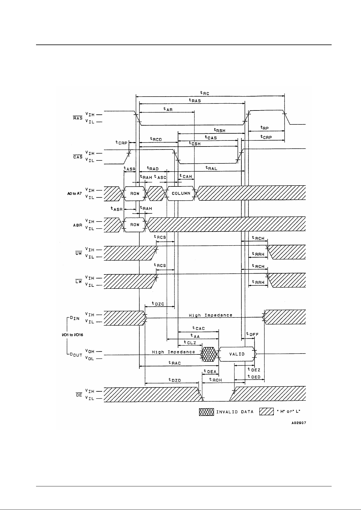
Read Cycle
No. 5085-7/29
LC322271J, M, T-70/80
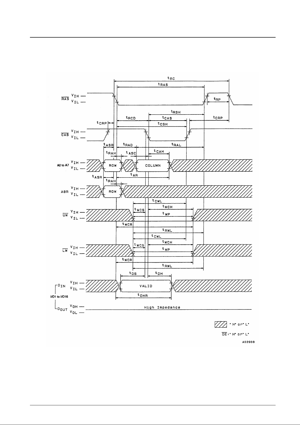
Early Write Cycle
No. 5085-8/29
LC322271J, M, T-70/80
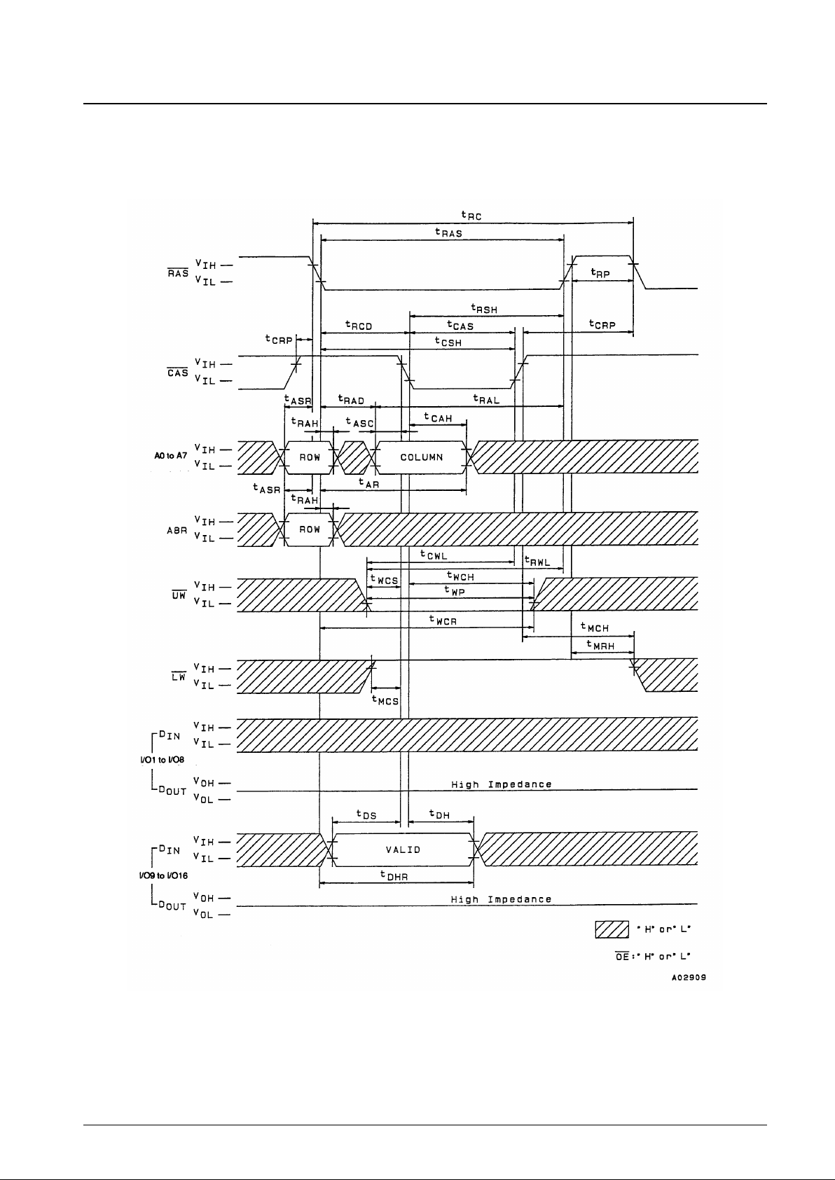
Upper Byte Early Write Cycle
No. 5085-9/29
LC322271J, M, T-70/80
 Loading...