

Page 1
Ordering number : EN4842
93098HA(OT)/81994TH (OT) B8-0889 No. 4842-1/13
Overview
The LA3460M is a high performance car stereo tuner IC
that includes an FM noise canceller and a stereo multiplex
demodulator.
Functions
[Noise Canceller Block]
• Built-in low- and high-pass filters
• Noise AGC
• Pilot signal compensation function
[Multiplex Block]
• Adjustment-free VCO (456 kHz)
• Level follower type pilot canceller
• SNC (stereo noise control)
• HCC (high cut control)
• Stereo indicator driver
• VCO oscillator stop function
Features
[Noise Canceller Block]
• Improved ignition noise rejection during medium to
weak field reception
Adoption of a new noise AGC circuit
Optimized gate time
• High audio quality design with malfunction prevention in
the high frequency band and for overmodulated signals
Improved dynamic range low-pass and high-pass filters
[Multiplex Block]
• High signal-to-noise ratio and low distortion (stereo S/N
ratio: 79 dB, THD: 0.1 %)
• Good high frequency band separation (50 dB at 1 kHz
and 30 dB at 10 kHz)
• Adoption of a PLL circuit with an adjustment-free VCO
(456 kHz ceramic resonator)
• Improved pilot cancellation level (25 to 30 dB) using a
new cancellation circuit
• Built-in 114 kHz and 190 kHz anti-birdie filters
• Adoption of new SNC characteristics to reduce
multipath noise
• Reduced printed circuit board space requirements due to
the adoption of a mini-flat package (MFP-24)
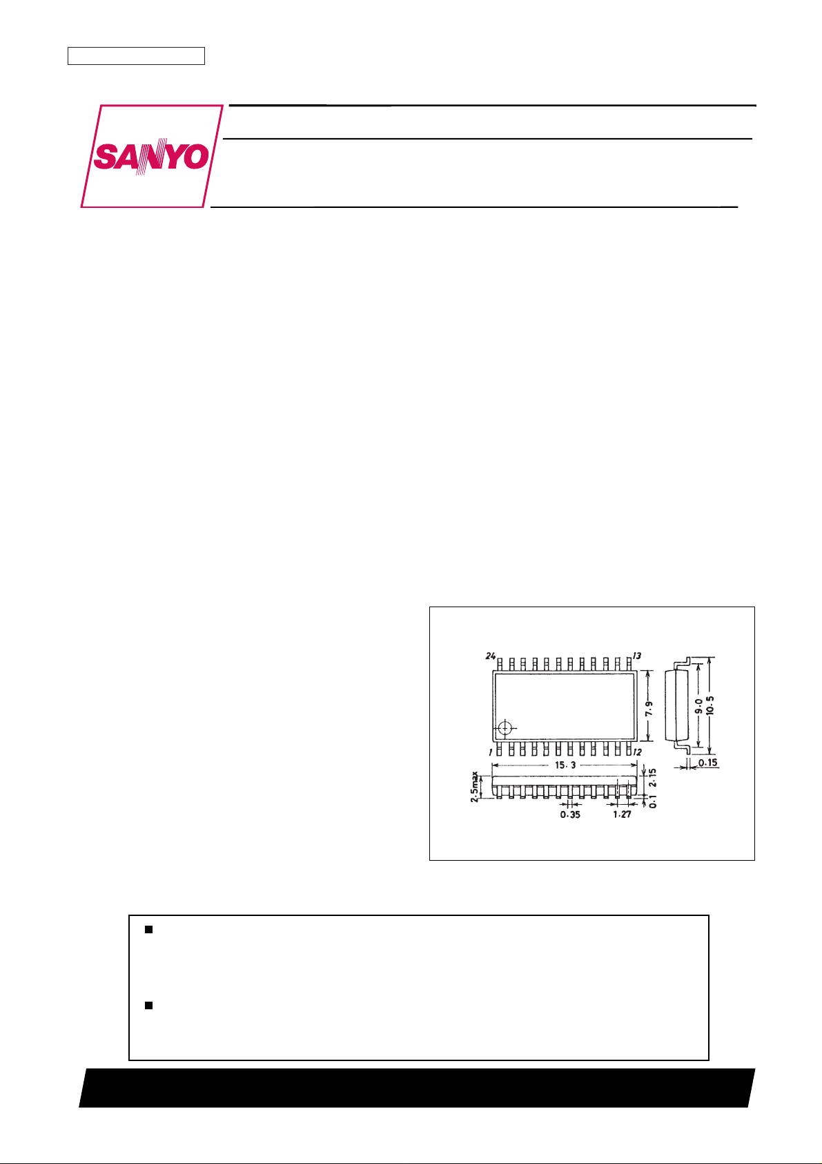
Package Dimensions
unit: mm
3045B-MFP24
SANYO: MFP24
[LA3460M]
LA3460M
FM NC + MPX Demodulator
for Car Stereo Tuners
Monolithic Linear IC
SANYO Electric Co.,Ltd. Semiconductor Bussiness Headquarters
TOKYO OFFICE Tokyo Bldg., 1-10, 1 Chome, Ueno, Taito-ku, TOKYO, 110-8534 JAPAN
Any and all SANYO products described or contained herein do not have specifications that can handle
applications that require extremely high levels of reliability, such as life-support systems, aircraft’s
control systems, or other applications whose failure can be reasonably expected to result in serious
physical and/or material damage. Consult with your SANYO representative nearest you before using
any SANYO products described or contained herein in such applications.
SANYO assumes no responsibility for equipment failures that result from using products at values that
exceed, even momentarily, rated values (such as maximum ratings, operating condition ranges, or other
parameters) listed in products specifications of any and all SANYO products described or contained
herein.
Page 2

Specifications
Maximum Ratings at Ta = 25°C
Operating Conditions at Ta = 25°C
Operating Characteristics
at Ta = 25°C, VCC= 8.0 V, VIN= 300 mVrms, f = 1 kHz, L + R = 90%, pilot = 10% modulation, VSNC (V8) = 3
V, VHCC (V9) = 3 V
No. 4842-2/13
LA3460M
Parameter Symbol Conditions Ratings Unit
Maximum supply voltage V
CC
max 10 V
Lamp influx current I
L
max 30 mA
Allowable power dissipation Pd max Ta = 85°C 490 mW
Operating temperature Topr –40 to +85 °C
Storage temperature Tstg –40 to +150 °C
Parameter Symbol Conditions
Ratings
Unit
min typ max
Quiescent current Icco No input 15 25 35 mA
Channel separation SEP 30 50 dB
Total harmonic distortion THD MONO 0.06 0.5 %
Lamp lit level V
L
Pilot signal 4.0 7.3 13.0 mVrms
Lamp hysteresis hy 3.0 6.0 dB
Demodulator output V
O
MONO 260 330 410 mVrms
S/N ratio S/N Rg = 0 Ω, MONO 70 85 dB
Channel balance CB MONO 20
× log (L/R) –1.0 0 +1.0 dB
Pilot cancellation PC 30 mVrms pilot signal 10 26 dB
Gate time tgate 1 µs 100 mVp-o, pulse input, f = 1 kHz 30 60 µs
Noise sensitivity S
N
1 µs pulse input, f = 1 kHz 30 60 mVp-o
SNC (1) V = 1.2 V, separation L → R 30 50 dB
SNC SNC (2) V = 0.6 V, separation L → R 6.0 8.5 11.0 dB
SNC (3) V = 0.1 V, separation L → R 0.5 2.0 dB
HCC (1) V = 1.2 V, f = 10 kHz, left output –1.0 0 +1.0 dB
HCC HCC (2) V = 0.6 V, f = 10 kHz, left output –8.0 –5.0 –2.0 dB
HCC (3) V = 0.1 V, f = 10 kHz, left output –14.0 –10.0 –6.0 dB
Parameter Symbol Conditions Ratings Unit
Recommended supply voltage V
CC
8.0 V
Operating supply voltage range V
CC
op 7.0 to 9.0 V
Page 3
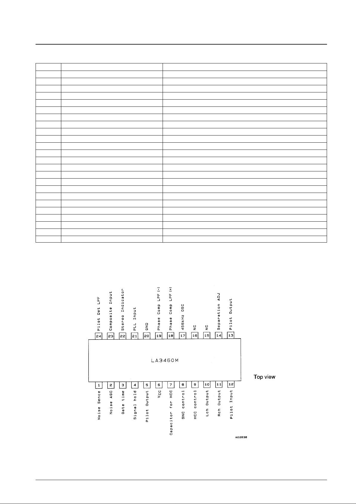
Pin Functions
Pin Assignment
No. 4842-3/13
LA3460M
Pin No. Function Description
1 Noise sensitivity Noises sensitivity adjustment
2 Noise AGC
3 Gate time
4 Hold circuit
5 Pilot output
6 V
CC
VCC= +8.0 V
7 HCC capacitor High cut filter
8 SNC control
9 HCC control
10 Left channel output
11 Right channel output
12 Pilot canceller input
13 Pilot canceller output
14 Separation adjustment
15 NC
16 NC
17 456 kHz oscillator circuit Ceramic resonator
18 Phase comparator L.P.F (+) Phase comparator low-pass filter
19 Phase comparator L.P.F (–) Phase comparator low-pass filter
20 GND
21 PLL input PLL input
22 Stereo indicator Active low
23 Composite input Composite signal input
24 Pilot detector lpf
Page 4
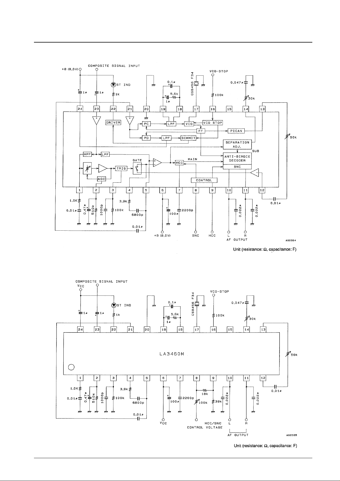
Equivalent Circuit Block Diagram
Sample Application Circuit
No. 4842-4/13
LA3460M
Page 5

Pin Functions
[NC]
No. 4842-5/13
LA3460M
Pin Function Internal equivalent circuit Remarks
23
1
2
3
Noise canceller input
Noise canceller
AGC sensitivity
adjustments
Monostable multivibrator
time constant
The input impedance is about 50 kΩ.
After setting up medium field (about 50 dBµ)
reception with the noise sensitivity setting pin
(pin 1), set up weak field (20 to 30 dBµ) reception
with the AGC adjustment pin (pin 2).
Set this time constant so that the gate time is
about 30 µs.
Increasing the gate time improves the noise
exclusion efficiency. However, care is required
since the apparent distortion due to multipath or
overmodulation will increase.
Continued on next page.
Unit (resistance: Ω, capacitance: F)
Page 6

Continued from preceding page.
No. 4842-6/13
LA3460M
Pin Function Internal equivalent circuit Remarks
4
5
12
Memory circuit connection
Pilot canceller signal input
Memory circuit used during noise canceller
operation
The pilot signal level requires adjustment due to
variations in the IF output level and other
parameters.
Unit (resistance: Ω, capacitance: F)
Page 7

[MPX]
No. 4842-7/13
LA3460M
Pin Function Internal equivalent circuit Remarks
21
7
20
10
11
Pilot input
HCC capacitor
N.C
MPX
GND
MPX output (left)
MPX output (right)
Pin 21 is the PLL circuit input.
The HCC frequency characteristics are determined
by the value of the external capacitor connected to
this pin.
Noise canceller and MPX circuit ground
Continued on next page.
Unit (resistance: Ω, capacitance: F)
Page 8

Continued from preceding page.
No. 4842-8/13
LA3460M
Pin Function Internal equivalent circuit Remarks
13
22
16
Pilot canceller signal input
Stereo indicator
OSC-stop
Pin 13 is the pilot canceller signal input.
Stereo indicator
This is an active-low signal.
Continued on next page.
Unit (resistance: Ω, capacitance: F)
Page 9

Continued from preceding page.
No. 4842-9/13
LA3460M
Pin Function Internal equivalent circuit Remarks
14
17
18
19
Separation adjustment
VCO
Phase comparator
The trimmer connected at this pin is used to adjust
the sub-decoder input level. (The output level in
mono (main) mode is not affected.)
The oscillator frequency is 456 kHz.
Continued on next page.
Unit (resistance: Ω, capacitance: F)
Page 10

Continued from preceding page.
No. 4842-10/13
LA3460M
Pin Function Internal equivalent circuit Remarks
9
8
24
HCC control input
SNC control input
Pilot detector
The sub-output is controlled by an input
between 0 and 1 V.
The circuit is forced to mono by the insertion of
a 1 MΩ resistor between pin 24 and V
CC
.
Unit (resistance: Ω, capacitance: F)
Page 11

Usage Notes
1. Noise Canceller Block
• The noise canceller input (pin 23) has an input impedance of about 50 kΩ. Carefully consider low-area frequency
characteristics when determining the value of the coupling capacitor. In an application circuit that uses a 1 µF
capacitor, fc will be about 3 Hz.
• Pins 1 and 2 are used to set the noise detector sensitivity and the noise AGC level. Setting up these values is easier
if the noise sensitivity is set with pin 1 for a medium field strength (an antenna input of about 50 dBµ) first, and
then the AGC is adjusted with pin 2 for a weak field strength (20 to 30 dBµ ). A point that requires caution is that
although the AGC action is improved if the noise detector sensitivity is increased, the weak field sensitivity will,
inversely, be lowered.
• The time constant of the monostable multivibrator (pin 3) will be about 30 µs when C is 0.001 µF and R is 100 kΩ.
The noise exclusion efficiency increases if the gate time is increased. However, distortion due to multipath and
overmodulation is increased.
2. MPX Block
• HCC (high cut control) frequency characteristics (pin 7)
The value of the external capacitor connected to pin 7 determines the output signal frequency characteristics during
HCC control.
No. 4842-11/13
LA3460M
Page 12

• Pilot canceller adjustment (pins 12 and 13)
The pin 13 pilot canceller signal waveform is a 19 kHz signal that does not include the third harmonic component,
as shown in the figure below. There is no need for a capacitor between pin 13 and ground, since this signal has the
same phase as the pilot signal. Since it does not include a third harmonic component, good pilot cancellation in the
left and right channel outputs can be obtained by adjusting the variable resistor.
• Separation adjustment (pin 14)
The separation is adjusted by varying the sub-decoder input level with the variable resistor connected to pin 14.
When the variable resistor is changed, only the sub-demodulation level is changed, and the mono (main) output
level is not changed. The decoder high band separation will not be degraded in the sub-signal frequency band
(23 to 53 kHz) if the value of the external capacitor C is made sufficiently small relative to the impedance of the
variable resistor.
No. 4842-12/13
LA3460M
Page 13

PS. No. 4842-13/13
LA3460M
This catalog provides information as of August, 1998. Specifications and information herein are subject to
change without notice.
Specifications of any and all SANYO products described or contained herein stipulate the performance,
characteristics, and functions of the described products in the independent state, and are not guarantees
of the performance, characteristics, and functions of the described products as mounted in the customer’s
products or equipment. To verify symptoms and states that cannot be evaluated in an independent device,
the customer should always evaluate and test devices mounted in the customer’s products or equipment.
SANYO Electric Co., Ltd. strives to supply high-quality high-reliability products. However, any and all
semiconductor products fail with some probability. It is possible that these probabilistic failures could
give rise to accidents or events that could endanger human lives, that could give rise to smoke or fire,
or that could cause damage to other property. When designing equipment, adopt safety measures so
that these kinds of accidents or events cannot occur. Such measures include but are not limited to protective
circuits and error prevention circuits for safe design, redundant design, and structural design.
In the event that any or all SANYO products (including technical data, services) described or contained
herein are controlled under any of applicable local export control laws and regulations, such products must
not be exported without obtaining the export license from the authorities concerned in accordance with the
above law.
No part of this publication may be reproduced or transmitted in any form or by any means, electronic or
mechanical, including photocopying and recording, or any information storage or retrieval system,
or otherwise, without the prior written permission of SANYO Electric Co., Ltd.
Any and all information described or contained herein are subject to change without notice due to
product/technology improvement, etc. When designing equipment, refer to the “Delivery Specification”
for the SANYO product that you intend to use.
Information (including circuit diagrams and circuit parameters) herein is for example only; it is not
guaranteed for volume production. SANYO believes information herein is accurate and reliable, but
no guarantees are made or implied regarding its use or any infringements of intellectual property rights
or other rights of third parties.
 Loading...