

Page 1

Any and all SANYO products described or contained herein do not have specifications that can handle
applications that require extremely high levels of reliability, such as life-support systems, aircraft’s
control systems, or other applications whose failure can be reasonably expected to result in serious
physical and/or material damage. Consult with your SANYO representative nearest you before using
any SANYO products described or contained herein in such applications.
SANYO assumes no responsibility for equipment failures that result from using products at values that
exceed, even momentarily, rated values (such as maximum ratings, operating condition ranges,or other
parameters) listed in products specifications of any and all SANYO products described or contained
herein.
Monolithic Linear IC
PLL FM MPX Stereo Demodulator with Adjustment-Free VCO
and Measure Against Adjacent Channel Interference
Ordering number:ENN2393
LA3450
SANYO Electric Co.,Ltd. Semiconductor Company
TOKYO OFFICE Tokyo Bldg., 1-10, 1 Chome, Ueno, Taito-ku, TOKYO, 110-8534 JAPAN
Overview
The LA3450 is a multifunctional, high-performance FM
multiplex demodulator IC designed for high-grade FM stereo tuner use. The LA3450 features adjustment-free VCO,
measure against adjacent channel interference, pilot canceler, low distortion (0.005%), and high S/N (101dB).
Applications
• Home stereo, CD, AV-use PLL FM MPX stereo demodulator IC with adjustment-free VCO.
Package Dimensions
unit:mm
3029A-DIP28S
[LA3450]
28
1
27.2
15
14
10.16
8.6
0.25
Functions
• PLL multiplex stereo demodulator.
• Adjustment-free VCO.
• Measure against adjacent channel interference.
• Pilot canceler.
• Cal-tone signal generator.
• AM/FM input, AM/FM selector.
• Post amplifier (gain variable type).
• VCO stop.
• Right/left independent adjustment of separation (single
adjustment available).
Features
• Adjustmet-free VCO : Eliminates the need to adjust freerunning frequency.
• Good temperature characteristics of VCO : ±0.1% typ.
for ±50°C change.
• No antibirdie filter is required because a measure is taken
against adjacent channel interference.
• Less carrier leak 19kHz : 53dB 38kHz : 50dB
• The on-chip cal-tone signal generator facilitates application of recording calibrator.
• Low distortion MONO 0.005% STEREO 0.015%
• High S/N 101dB typ. MONO IHF-A BPF
• High voltage gain FM : 10dB (gain variable)
AM : 16dB (gain variable)
• Wide dynamic range Output level 3.3V typ. (THD=1%,
MONO)
2.03 1.78
0.48
0.95
4.25
4.95max
3.2
0.51min
SANYO : DIP28S
21500TH (KT)/2187TA No.2393–1/15
Page 2

LA3450
Specifications
Absolute Maximum Ratings at Ta = 25˚C
retemaraPlobmySsnoitidnoCsgnitaRtinU
egatloVylppuSmumixaMV
tnerruCevirDpmaLI
noitapissiDrewoPelbawollAxamdP 086Wm
erutarepmeTgnitarepOrpoT 07+ot02–
erutarepmeTegarotSgtsT 521+ot04–
Operating Conditions at Ta = 25˚C
retemaraPlobmySsnoitidnoCsgnitaRtinU
egatloVylppuSdednemmoceRV
egatloVgnitarepOV
egatloVlangiStupnIdednemmoceRV
Electrical Characteristics at Ta = 25˚C, VCC=13V, Input : 400mV, f=1kHz, L+R=90%, pilot=10%
retemaraPlobmySsnoitidnoC
tnerruCtnecseiuQoccItupnioN9293Am
ecnatsiseRtupnIirnommoctupniMA,MF410262kΩ
noitarapeSlennahCpeS
noitrotsiDcinomraHlatoTDHT
leveLtupnIelbawollAxamniV
egatloVtuptuOoV
oitaResioN-ot-langiSN/SFPBA-FHIONOM09101Bd
noitcejeResioNeidriBRBzHk511=sf,Vm001=SV,langissuoirupS04Bd
kaeLreirraCzHk91LC
kaeLreirraCzHk83LC
klatssorCTC
ecnalaBlennahCBCONOMMF01Bd
ycneuqerFCSOenot-laC 004zH
egatloVtceleSMF/MAV
egatloVpotSOCV 01nipotdeilppaegatloV5.2V
leveLgnithgiLpmaLV
siseretsyHpmaLyh 5.3Bd
)1etoN(egnaRerutpaC Vm03TOLIP2.1±%
(Note 1) : The capture range is represented by the value in 19kHz equivalent.
(Note 2) : The low-pass filter used to measure electrical characteristics must have 19kHz attenuation of –90dB or more
negative value of dB and 38kHz attenuation of –70dB or more negative value of dB.
(Note 3) : Be carefull that the combination of pin 22 ⊕ and the others causes dielectric breakdown easily.
xam 61V
CC
xam 03Am
L
˚C
˚C
CC
po 51ot01V
CC
i
nimpytxam
zH001=f05Bd
zHk1=f5406Bd
zHk01=f05Bd
ONOMMF500.050.0%
NIAMMF510.080.0%
tupniVm002MA20.080.0%
%1=DHT,ONOMMF0080021Vm
MA004006Vm
ONOMMF07700110051Vm
tupniVm002MA07700110051Vm
91
83
MA → Vm002tupniMA,MF0708Bd
MF → Vm004tupniMF,MA0708Bd
MA → 62nipotdeilppaegatlov,MF5.0V
MF-MA
MF → 62nipotdeilppaegatlov,MA5.2V
L
sisahpme-eD05Bd
sisahpme-ed,relecnaC35Bd
LEVELTOLIP45.731Vm
31V
004Vm
sgnitaR
tinU
No.2393–2/15
Page 3
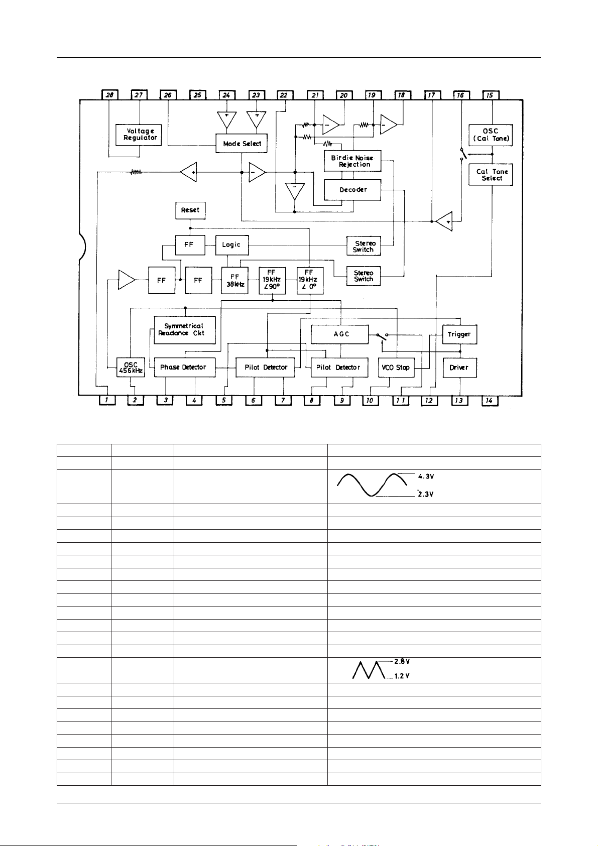
Internal Block Diagram
LA3450
Typical Value of Voltage on Each Pin and Pin Name
.oNniPeulaV.pyTemaNniPskrameR
1V7.5tuptuoreifilpmaetisopmoCk1ecnatsisertuptuO Ω
2–CSO
3V6.2retlifpooL
4V6.2retlifpooL
5V6.2tupniLLP
6V6.2retlifnoitcetedcnystoliP
7V6.2retlifnoitcetedcnystoliP
8V6.2retlifnoitcetedcnystoliPlecnactoliproF
9V6.2retlifnoitcetedcnystoliPlecnactoliproF
01– potsOCVk021ecnatsisertupnI Ω
11– lecnactoliP pu-wolloflevel,tuptuoevawralugnairT
21V8.3lortnocenot-laC .etatsNOtaegatlovybdetneserpersiegatlovniP
31– rotacidnioeretSrotcellocnepO
410DNG
51– tuptpuoCSOenot-laC
61V7.5tupnienot-laC
71V7.5tupnilecnactoliP
81V7.5tuptuorefilpmatsoPtuptuoL
91V7.5tupnireifilpmatsoPtupni)–(,tupniL
02V7.5tuptuorefilpmatsoPtuptuoR
12V7.5tupnireifilpmatsoPtupni)–(,tupniR
22V7.5tnemtsujdanoitarapeS
32V7.5tupniMAk02ecnatsisertupnI Ω
f≅456kHz
f≅400Hz
Continued on next page.
No.2393–3/15
Page 4
LA3450
Continued from preceding page.
.oNniPeulaV.pyTemaNniPskrameR
42V7.5tupniMFk02ecnatsisertupnI Ω
520 DNGlangiS
62– noitcelesMF/MAk021ecnatsisertupnI Ω
72V7.5ferVegatlovecnerefeR
82V
CC
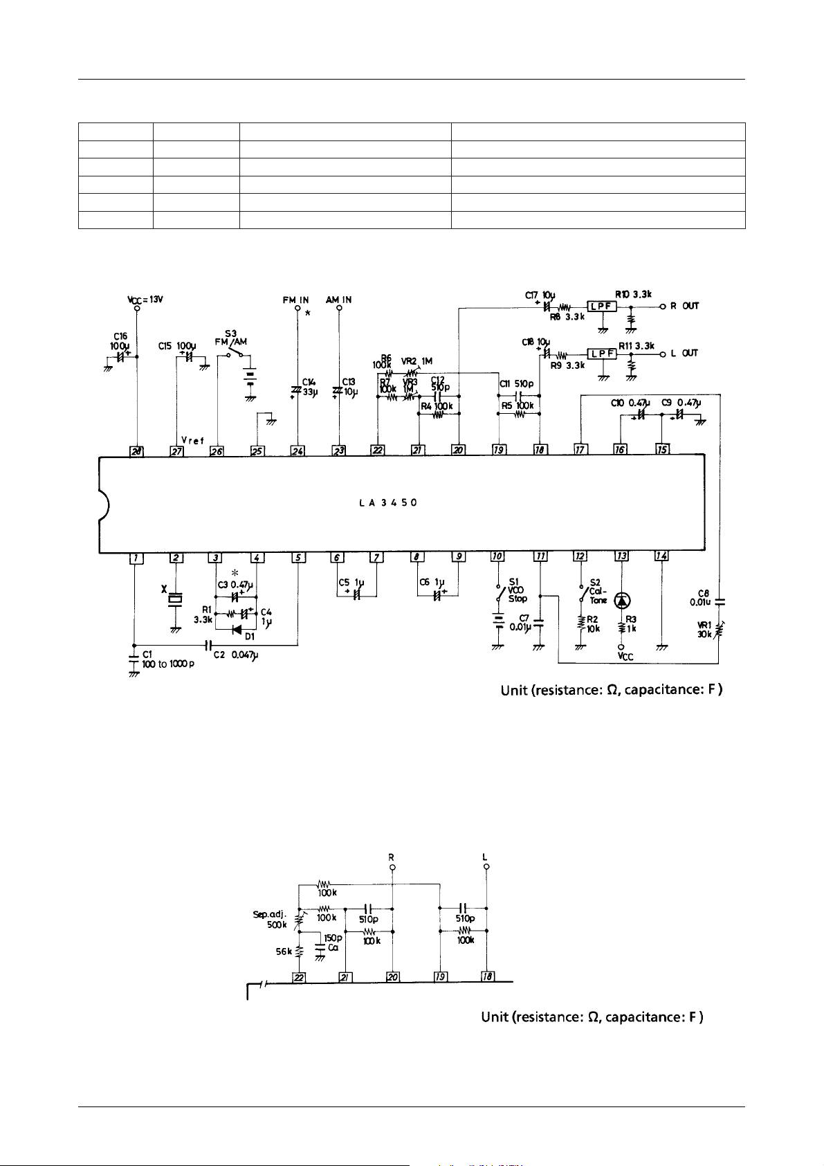
Sample Application Circuit (1)
Input separation ≥ 0.92
ylppusrewoP
X : CSB456F11 (Murata)
KBR-457HS (Kyocera)
* : Input pilot level 20mV or greater : 0.47µF
14mV or greater : 0.22µF
8mV or greater : C3=0.1µF, R1=6.8kΩ, C4=0.47µF
* : Input separation (sub signal/main signal) ≥ 0.92 (f=1kHz)
How to Make Single Adjustmet of Separation
No.2393–4/15
Page 5
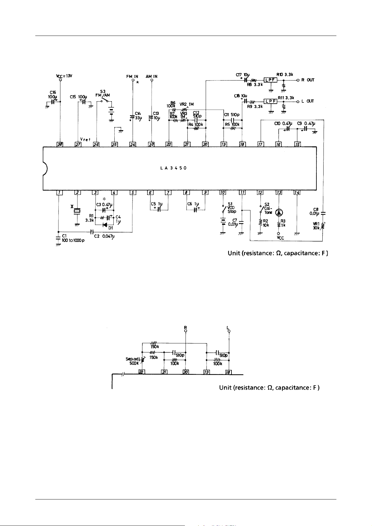
Sample Application Circuit (2)
Input separation ≤ 0.92
LA3450
X : CSB456F11 (Murata)
KBR-457HS (Kyocera)
* : Input pilot level 20mV or greater : 0.47µF
14mV or greater : 0.22µF
8mV or greater : C3=0.1µF, R1=6.8kΩ, C4=0.47µF
* : Input separation (sub signal/main signal) ≥ 0.92 (f=1kHz)
How to Make Single Adjustmet of Separation
No.2393–5/15
Page 6

Sample Application Circuit (3)
Pilot sine wave cancel
LA3450
X : CSB456F11 (Murata)
KBR-457HS (Kyocera)
* : Input pilot level 20mV or greater : 0.47µF
14mV or greater : 0.22µF
8mV or greater : C3=0.1µF, R1=6.8kΩ, C4=0.47µF
* : Input separation (sub signal/main signal) ≤ 0.92 (f=1kHz)
For the separation adjusting method when the input separation is more than 0.92, see Sample Application Circuit (2).
(Note 1) In this Sample Application Circuit, the DC voltage on pins 11, 17 is almost equal to that on pin 27 and no DC cut
capacitor (C8 in Sample Application Circuint (1) , (2) ) is required.
No.2393–6/15
Page 7

LA3450
Description of External Parts
Name Symbol Kind Value Remarks
Capacitor C1 Ceramic 100 to 1000pF Inprovement in stereo low-frequency distortion
(Note1)
C2 Polyester film 0.047µF DC cut
C3 Electrolytic 0.1 to 0.47µF Loop filter, Input pilot 8mV or greater : 0.1µF
14mV or greater : 0.22µF
20mV or greater : 0.47µF
C4 Electrolytic 0.47µF to 1µF Loop filter, Input pilot 8mV or greater : 0.47µF
14mV or greater : 1µF
C5 Electrolytic 1µF Sync detection filter
C6 Electrolytic 1µF Sync detection filter
C7 Polyester film 0.01µF For integration (generation of triangular wave)
C8 Polyester film 0.01µF DC cut
C9 Electrolytic 0.47µF For integration (generation of triangular wave)
C10 Electrolytic 0.47µF DC cut
C11 to 12 Ceramic 510pF De-emphasis capacitor, R5. C11=50µs (75µs)
R4. C12=50µs (75µs)
C13 Electrolytic 10µF DC cut
C14 Electrolytic 33µF DC cut
C15 Electrolytic 100µF Filter, S/N improvement
C16 Electrolytic 100µF Power filter
C17 to 18 Electrolytic 10µF DC cut
C19 Ceramic 1000pF LPF for sub signal attenuation
C20 to 21 Ceramic 100pF Improvement in separation at high frequencies (Note 2)
C22 Ceramic 4700pF 19kHz tank circuit (generation of sine wave)
Resistor R1 Carbon 3.3 to 6.8kΩ Loop filter, Input pilot 8mV or greater : 6.8kΩ
14mV or greater : 3.3kΩ
R2 Carbon 10kΩ Fixing of cal-tone OSC frequency
R3 Carbon 1kΩ Limiting resistor
R4 to 5 Carbon 100kΩ Post amplifiler feedbak resistor, de-emphasis resistor
R6 to 7 Carbon 100kΩ For separation adjustment
R8 to 9 Carbon 3.3kΩ LPF input resistor (Note 3)
R10 to 11 Carbon 3.3kΩ LPF output resistor
R12 Carbon 2kΩ LPF for sub signal attenuation
R13 Carbon 10kΩ Generation of pilot cancel signal
Semifixed VR1 Carbon 30kΩ Pilot cancel adjustment
resistor VR2 to 3 Carbon 1MΩ Separation adjustment
Resonator X Ceramic CSB456F11 (Murata), KBR-457HS (Kyocera)
Diode D1 Silicon (Low leak) Improvement in stereo start time after VCO stop release
Coil L1 15mH 19kHz tank circuit (generation of sine wave)
Note 1 : C1 differs with set models. Capacitor used to phase the sub signal of the decoder with the reproduction sub signal
in the PLL.
Note 2 : C20 to 21 are set to the optimum value according to each set mode.
Note 3 : The LPF input resistor value is 3.3kΩ or greater.
No.2393–7/15
Page 8

Sample Printed Circuit Pattern
LA3450
Proper Cares in Applications
1. Ceramic resonator
Shown below are ceramic resonators recommended for use in the LA3450 and their suppliers.
CSB456F11 Murata Piezoelectric Division
TEL : 0762-40-2381
KBR-457HS Kyocera Electronic Parts Division
TEL : 075-592-3851
2. Loop filter constants
Loop filter constants (C3, C4, R1) connected to pins 3, 4 must be set to the optimum value according to an input pilot
level. The recommended values are shown in Table 1.
leveLtoliPtupnI3C4C1R
retaergroVm02Fµ74.0Fµ1k3.3 Ω
retaergroVm41Fµ22.0Fµ1k3.3 Ω
retaergroVm8Fµ1.0Fµ74.0k8.6 Ω
Table 1. Input Pilot Level – Loop Filter Constants
Note : For example, when the loop filter constants are C3=0.22µF, C4=1µF, R1=3.3kΩ, stereo operation can be per-
formed with an input pilot level of 14mV or greater, even with the temperature characteristics of the OSC
circuit, the initial tolerance and secular chage of a ceramic resonator considerd.
No.2393–8/15
Page 9

LA3450
3. VCO stop method
VCO OSC can be stopped and the forced monaural mode is entered by applying a voltage of 2.5V or greater to pin 10.
The maximum voltage to be applied to pin 10 is 16V regardless of the voltage on pin 28 (VCC pin). The relation
between applied voltage and flow-in current is shown in Fig. 1.
Fig. 1. Voltage Applied to pins 10, 26 – Flow-in Current
4. Forced monaural mode
Connecting pin 16 to GND through a resistor of 10kΩ causes the forced monaural mode to be entered.
5. AM/FM mode select method
The AM/FM mode can be selected by applying a v oltage to pin 26. When the voltage on pin 26 is 0.5V or less, the FM
mode is entered, and when 2.5V or greater, the AM mode is enterd. In AM mode the VCO stops and the forced
monaural mode is entered. The relation between voltage on pin 26 and flow-in current is as shown in Fig. 1.
6. Separation adjust method
The separation is adjusted by varying the gain of the main signal with VR2, VR3 as shown in the Sample Application
Circuit. Sample Application Circuit (1) or (2) is used according to the attenuation of the input sub signal. When the
attenuation ratio of the sub signal to the main signal is 0.92 or greater to 1, use Sample Application Circuit (1), and
when 0.92 or less to 1, use Sample Application Circuit (2). Capacitors C20 and C21, which are used to improve the
separation characteristic at high frequencies, must be set to the optimum values according to your model set.
7. Cal-tone
The OSC frequency can be set with R2, C9 in the Sample Application Circuit (refer to Fig. 2). The OSC level can be
attenuated on connecting resistor Rx across pin 15 and pin 16 (refer to Fig. 3). When tthe S2 is turned on, the triangular
wave generated on pin 15 is amplified by the post amplifier and output. The level at pins 18, 20 is approximately 4V
(p-p) when the typical constants are used in the Sample Application Circuit and the output level becomes approximately 4X20/ (Rx+20) V (p-p) by connecting Rx.
Fig. 3. OSC Level Variable
No.2393–9/15
Page 10

LA3450
8. VO – IO characteristic at pin 27
Fig. 4 shows VO – IO characteristic at pin 27 (IO : Capable of being drawn to the outside)
Maximum current : 3mA
9. Feedback resistance of post amplifier and total gain, de-emphasis constants
Table 2 shows the feedback resistance of post amplifier and the total gain, de-emphasis constants.
)5R(4RniaglatoTsµ05)11C(21Csµ05)11C(21C
k33 Ω Bd0Fp0051Fp0022
k93 Ω Bd5.1Fp0021Fp0002
k15 Ω Bd4Fp0001Fp0051
k26 Ω Bd5.5Fp057Fp0021
k28 Ω Bd8Fp026Fp019
k001 Ω Bd01Fp015Fp057
k031 Ω Bd21Fp093Fp065
k051 Ω Bd31Fp033Fp015
k081 Ω Bd51Fp072Fp093
Total gain : At monaural mode, R4 · C12=R5 · C11=50µs, 75µs
Table 2. Feedback resistance of post amplifier and of total gain, de-emphasis constants
10. Low-pass filter
Figs. 5, 6 show a sample circuit configuration and characteristic of the low-pass filter.
Fig. 5 Sample Circuit of LC Filter
No.2393–10/15
Page 11

LA3450
Fig. 6 f Response
Note : As the use of this low-pass filter makes the attenuation less at 19kHz, 38kHz, carrier leak at the LPF output
causes the stereo distortion and separation characteristics to get worse than specified in the Electric Character istics. For example, the stereo distortion becomes approximately 0.5% due to carrier leak.
No.2393–11/15
Page 12

LA3450
No.2393–12/15
Page 13

LA3450
No.2393–13/15
Page 14

LA3450
No.2393–14/15
Page 15

LA3450
Specifications of any and all SANYO products described or contained herein stipulate the performance,
characteristics, and functions of the described products in the independent state, and are not guarantees
of the performance, characteristics, and functions of the described products as mounted in the customer's
products or equipment. To verify symptoms and states that cannot be evaluated in an independent device,
the customer should always evaluate and test devices mounted in the customer's products or equipment.
SANYO Electric Co., Ltd. strives to supply high-quality high-reliability products. However, any and all
semiconductor products fail with some probability. It is possible that these probabilistic failures could
give rise to accidents or events that could endanger human lives, that could give rise to smoke or fire,
or that could cause damage to other property. When designing equipment, adopt safety measures so
that these kinds of accidents or events cannot occur. Such measures include but are not limited to protective
circuits and error prevention circuits for safe design, redundant design, and structural design.
In the event that any or all SANYO products(including technical data,services) described or
contained herein are controlled under any of applicable local export control laws and regulations,
such products must not be exported without obtaining the export license from the authorities
concerned in accordance with the above law.
No part of this publication may be reproduced or transmitted in any form or by any means, electronic or
mechanical, including photocopying and recording, or any information storage or retrieval system,
or otherwise, without the prior written permission of SANYO Electric Co. , Ltd.
Any and all information described or contained herein are subject to change without notice due to
product/technology improvement, etc. When designing equipment, refer to the "Delivery Specification"
for the SANYO product that you intend to use.
Information (including circuit diagrams and circuit parameters) herein is for example only ; it is not
guaranteed for volume production. SANYO believes information herein is accurate and reliable, but
no guarantees are made or implied regarding its use or any infringements of intellectual property rights
or other rights of third parties.
This catalog provides information as of February, 2000. Specifications and information herein are subject
to change without notice.
PS No.2393–15/15
 Loading...