

Page 1
Any and all SANYO products described or contained herein do not have specifications that can handle
applications that require extremely high levels of reliability, such as life-support systems, aircraft’s
control systems, or other applications whose failure can be reasonably expected to result in serious
physical and/or material damage. Consult with your SANYO representative nearest you before using
any SANYO products described or contained herein in such applications.
SANYO assumes no responsibility for equipment failures that result from using products at values that
exceed, even momentarily, rated values (such as maximum ratings, operating condition ranges,or other
parameters) listed in products specifications of any and all SANYO products described or contained
herein.
Monolithic Linear IC
FM Noise Canceller
Ordering number:ENN855F
LA2110
SANYO Electric Co.,Ltd. Semiconductor Company
TOKYO OFFICE Tokyo Bldg., 1-10, 1 Chome, Ueno, Taito-ku, TOKYO, 110-8534 JAPAN
Overview
The LA2110 has the capability to effectively remove external noise (pulse noise) caused by engine, etc. and is used
in conjunction with a PLL FM multiplex stereo demodula-
tor (such as LA3375) with pilot signal canceller.
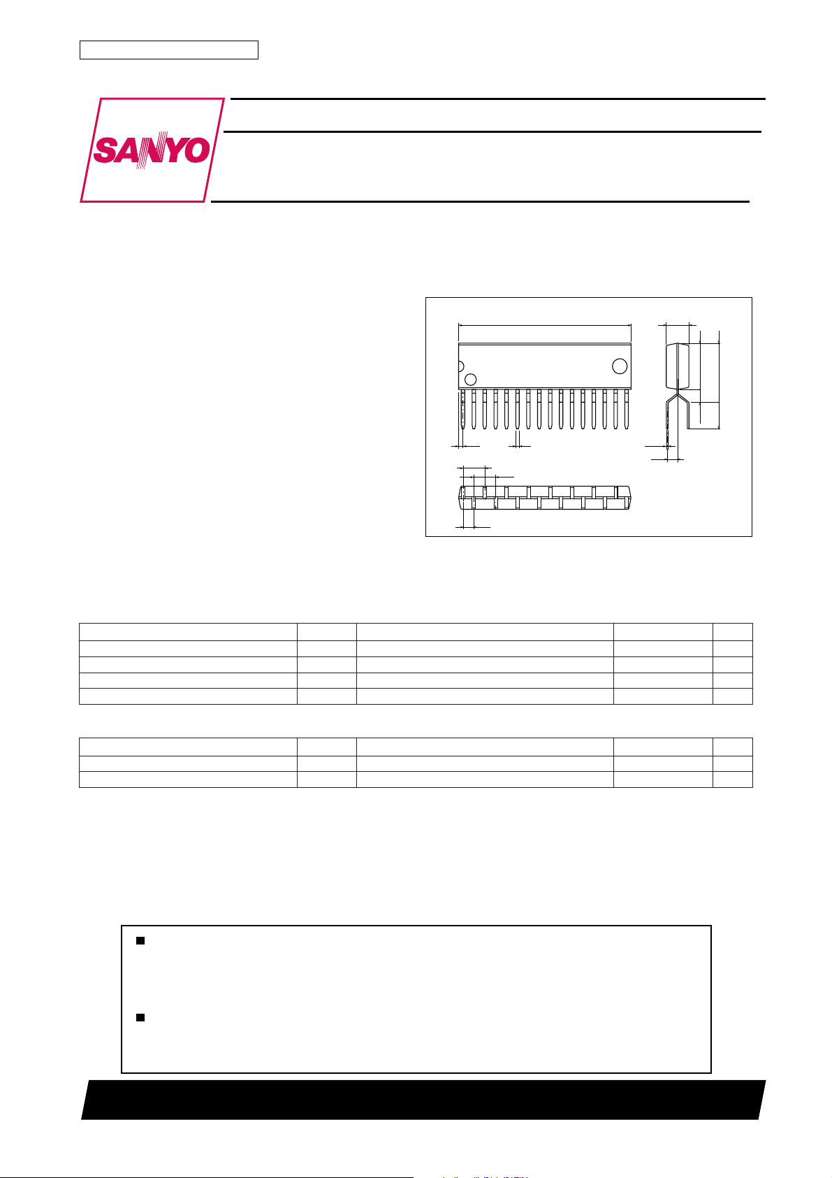
Package Dimensions
unit:mm
3193-SIP16Z
[LA2110]
24.2
3.25
Features
• Pilot signal compensation function.
• By using in conjunction with PLL FM multiplex stereo
demodulator with pilot signal canceller, adverse effect
caused by pilot signal can be compensated.
• Low distortion factor : THD=0.02%, 300mV.
• Good space facator due to single end package.
• Variable input type noise A GC system. This system widens the noise detector’s dynamic range, so that pulse noise
can be satisfactorily detected even in a weak electric field ,
and pulse noise is removed without adversely affecting
distortion factor.
Specifications
Absolute Maximum Ratings at Ta = 25˚C
retemaraPlobmySsnoitidnoCsgnitaRtinU
egatloVylppuSmumixaMV
noitapissiDrewoPelbawollAxamdP 054Wm
erutarepmeTgnitarepOrpoT 57+ot02–
erutarepmeTegarotSgtsT 521+ot04–
Recommended Operating Conditions at Ta = 25˚C
retemaraPlobmySsnoitidnoCsgnitaRtinU
egatloVylppuSdednemmoceRV
egnaRegatloVgnitarepOV
xam 61V
CC
Ta≤50˚C
CC
po 51ot8V
CC
6.5
8.8max
3.6
116
0.85
3.0
1.5
0.5
3.0
0.25
1.5
SANYO : SIP16Z
2.2min
˚C
˚C
21V
11200TH (KT)/D247KI/4115KI, TS No.855–1/6
Page 2
LA2110
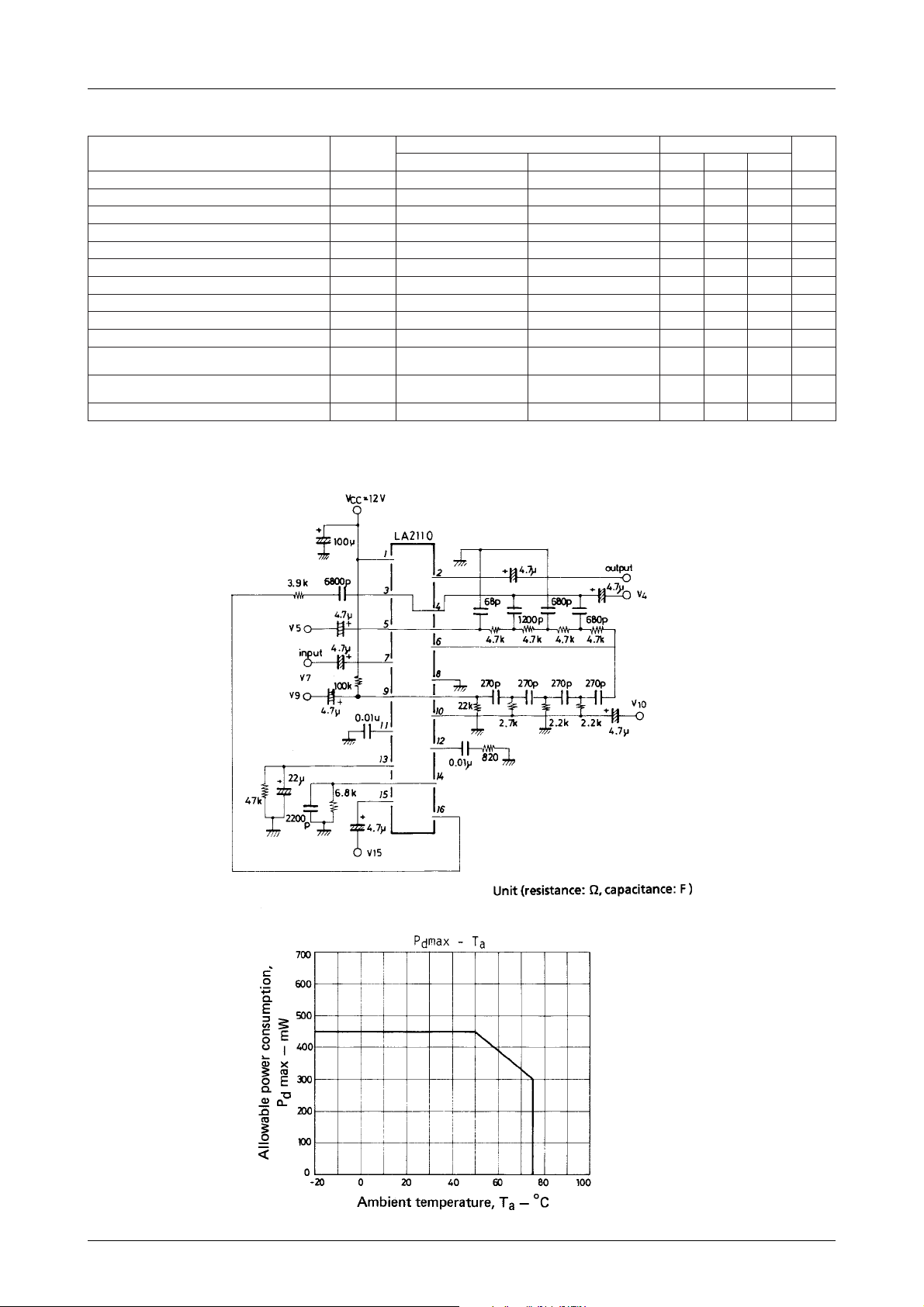
Operating Conditions at Ta = 25˚C, VCC=12V, See specified Test Circuit
snoitidnoCsgnitaR
4
01
DNGotdetrohs
niaGegatloVGVV
emiTetaGt
Test Circuit
retemaraPlobmyS
tnarruCtnecseiuQoccI 6152Am
egnaRcimanyDlangiStupnIV
ecnadepmItupnIZ
noitrotsiDcinomraHlatoTDHTV
niaGpmAssap-woLGV
niaGpmAssap-hgiHHGVV
rotcaFnoitrotsiDpmAgnitrevnIDHT
egnaRcimanyDpmAgnitrevnIDV
niaGpmAgnitrevnIGV
egatloVesioNtuptuOV
ytivitisneSesioNS
7
V
D
7
V
ni
7
7
V
L
5
9
V
I
51
V
I
51
V
I
51
V7V,
ON
etag
N
51
V
7
zHk1=f
V
7
)niptupni()niptuptuo(nimpytxam
zHk1=f,Vm003=tuptuO2.0–8.0+8.1+Bd
zHk1=f,%1=DHT,tuptuO3.1V
zHk1=f,Vm003=k63k15k76
zHk1=f,Vm003=tuptuO10.030.0%
zHk1=f,Vm003=V
zHk002=f,Vm001=V
zHk91=f,Vm001=tuptuO1.0%
zHk91=f,%1=DHT,tuptuO003Vm
zHk91=f,Vm001=tuptuO0.13.16.1semit
,sµ1,p-pVm001=
zHk1=f,sµ1,tuptuO03o-pVm
0.11.12.1semit
2.14.156.1semit
zHk001,tuptuO
retlifssap-wol
tuptuO311203sµ
0306Vµ
tinU
Ω
No.855–2/6
Page 3

Equivalent Circuit Block Diagram
LA2110
No.855–3/6
Page 4

LA2110
[Theory of LA2110 Noise Canceller]
In order to simplify the operation theory , the composite signal component is given only as a low frequency signal and a
pilot cancel signal has the same phase, same amplitude as the pilot signal in the composite signal.
Since the output voltage is the differential v oltage of the plus and minus input of the subtraction circuit, it is equal to the
voltage between the memory capacitor terminals. When the gate is closed, the composite signal is applied to the plus input
terminal of the subtraction circuit, and the pilot cancel signal is applied to the minus input terminal. Thus the pilot signal
is cancelled from the output and only the low frequency signal appears. In the same way, the voltage between the memory
capacitor terminals is the differential voltage of the composite signal and the pilot cancel signal, so only the low frequency
signal appears.
When pulse noise is generated and the gate opens, the plus input and minus input signal waveforms of the subtraction
circuit become equal. This is because the input impedance of the subtraction circuit is extremely high, so the memory
capacitor is considered AC-shorted. Thus, when pulse noise is generated in the composite signal, the same pulse noise
appears in minus as well as plus input of the subtraction circuit. As a result, pulse noise does not appear in the output. The
voltage in the output has a DC level difference of plus and minus input, and that is the voltage held by the memory
capacitor. This v oltage is that between the memory capacitor terminals just before the gate opens, so it is the lo w frequenc y
signal voltage just before the gate opens. Because the subtraction circuit input impedance is high, no charge/discharge
current flows in the memory capacitor while the gate is open, so the memory capacitor can hold the voltage between its
terminals.
The voltage waveforms are illustrated below.
Note : The pilot cancel signal is given as sinusoidal in this explanation, but in the actual application
circuit, pilot cancel is performed by a triangular wave.
No.855–4/6
Page 5

Sample Application Circuit : LA2110 & LA3375
LA2110
Note : When using the sample application circuit :
1. Separation adjustment is performed with 10kΩ variable resistance in low-pass filter.
2. Change noise detection sensitivity control RS to an adequate value for strong or medium electric field.
3. Adjust noise AGC with CY, RY for effective noise suppression in a medium or weak electric field.
4. Adjust pilot cancel degree with variable resistance of 50kΩ connected to LA2110 pin 15.
5. By changing the 1µF capacitor between LA3375 pin 11 and 12, pilot cancel follow-up response time can be changed.
But if the value is decreased, distortion factor, etc. will be adversely affected.
No.855–5/6
Page 6

LA2110
Specifications of any and all SANYO products described or contained herein stipulate the performance,
characteristics, and functions of the described products in the independent state, and are not guarantees
of the performance, characteristics, and functions of the described products as mounted in the customer's
products or equipment. To verify symptoms and states that cannot be evaluated in an independent device,
the customer should always evaluate and test devices mounted in the customer's products or equipment.
SANYO Electric Co., Ltd. strives to supply high-quality high-reliability products. However, any and all
semiconductor products fail with some probability. It is possible that these probabilistic failures could
give rise to accidents or events that could endanger human lives, that could give rise to smoke or fire,
or that could cause damage to other property. When designing equipment, adopt safety measures so
that these kinds of accidents or events cannot occur. Such measures include but are not limited to protective
circuits and error prevention circuits for safe design, redundant design, and structural design.
In the event that any or all SANYO products(including technical data,services) described or
contained herein are controlled under any of applicable local export control laws and regulations,
such products must not be exported without obtaining the export license from the authorities
concerned in accordance with the above law.
No part of this publication may be reproduced or transmitted in any form or by any means, electronic or
mechanical, including photocopying and recording, or any information storage or retrieval system,
or otherwise, without the prior written permission of SANYO Electric Co. , Ltd.
Any and all information described or contained herein are subject to change without notice due to
product/technology improvement, etc. When designing equipment, refer to the "Delivery Specification"
for the SANYO product that you intend to use.
Information (including circuit diagrams and circuit parameters) herein is for example only ; it is not
guaranteed for volume production. SANYO believes information herein is accurate and reliable, but
no guarantees are made or implied regarding its use or any infringements of intellectual property rights
or other rights of third parties.
This catalog provides information as of January, 2000. Specifications and information herein are subject
to change without notice.
PS No.855–6/6
 Loading...